Tunable and Dual-broadband Giant Enhancement of SHG and THG in a Highly-engineered Graphene-Insulator-Graphene Metasurface
Abstract
We demonstrate a novel scheme to dramatically enhance both the second- and third-harmonic generation in a graphene-insulator-graphene metasurface. The key underlying feature of our approach is the existence of a double-resonance phenomenon, namely the metasurface is designed to possess fundamental plasmon resonances at both the fundamental frequency and the higher harmonic. In particular, this dual resonant field enhancement at the two optical frequencies, combined with a favorable spatial overlap of the optical near-fields, lead to the increase of the generated higher harmonic by several orders of magnitude. Remarkably, we demonstrate that by tuning the Fermi energy of the graphene gratings the dual-resonance property can be locked-in over a broad spectral range of , and equally important, the enhanced nonlinear frequency generation process can be readily switched in the same device between the second and third harmonic. This new type of graphene metasurface could open up new avenues towards the development of novel ultra-compact and multi-frequency active photonic nanodevices.
The first successful isolation of graphene from graphite ngm04sci via mechanical exfoliation has opened up a rapidly growing field of research bsl06sci ; gn07natmat ; bgb08nanolet ; han08jap ; cgp09rmp , primarily due to the unique and remarkable properties of this new two-dimensional material. In its early stages research on graphene focused on its electronic and mechanical properties, but it was soon realized that key optical properties, such as extreme optical near-field confinement induced by the excitation of surface-plasmon polaritons (SPPs) gpn12natpho ; cbg12n ; fra12nat ; aba14acsphoto ; kca11nanolet ; cba12nat ; bfp13intjmodphyb , tunability of the optical response via gate voltage and chemical doping lyu11nat ; cry11nanotod ; bjs13nanolet , and low losses at high carrier densities dyml10NatNano ; la14AcsNano , could transform graphene into a promising and versatile material platform for a broad array of optoelectronic applications. To this end, photonic devices based on graphene, including diffractive elements, optical sensors, topological photonic devices, photovoltaic and photoresistive devices bsh10natpho ; bl12acsnano ; ybbp18Nanophoto ; ylet19NatNano ; ldj10sci ; kjbm18NanoLett ; xml09natnano ; sll10acsnano ; pls10optexp ; hygk19natcomm ; jlbp20JSTQE ; jcsf17PRL ; pyxa17NatComm , have already been demonstrated.
In addition to advances in exploiting the linear physics of graphene, its nonlinear optical properties could play an equally important role in key applications. Due to the centrosymmetric nature of graphene, the leading non-vanishing nonlinear optical interactions in graphene are of third-order type, such as third-harmonic generation (THG) and Kerr effect. In particular, it has been demonstrated that the strength of third-order nonlinear optical interactions in graphene is several orders of magnitude larger than in typical semiconductors hhm10prl ; hdp13prx ; cvs14newjphy ; csa16acsnano . More importantly, these nonlinear optical interactions can be further enhanced upon resonant excitation of SPPs in graphene structures, which leads to a number of exciting applications bsh10natpho ; bl12acsnano ; ybbp18Nanophoto ; wp16prb ; yywp17ptrsa ; vcg13optlet ; nan13lpr ; dyp15prb ; dcm15scirep ; sgisk13prb ; Soa18NatNano ; snsk15prb ; ylp20SciAdv , including frequency mixing bsh10natpho , photodetectors xml09natnano , generation of spatial solitons nan13lpr ; snsk15prb , physical systems with tunable Dirac points dyp15prb , and Anderson light localization at the nanoscale dcm15scirep .
Although the second-harmonic generation (SHG) is generally forbidden in a free-standing graphene sheet, it is nevertheless permitted in two main configurations. First, SHG does arise in graphene nanostructures from nonlocal effects csa16acsnano ; smki14prb ; msa15njp , namely when nonlinear sources of SHG are magnetic dipoles and electric quandrupoles. Second, by placing a graphene sheet on a substrate, the inversion symmetry of the system is broken and SHG due to local nonlinear polarization (electric dipoles) can occur gla11jlet ; mik11prb ; chc16natphy ; dh09apl ; dh10prb ; ard14prb . Under these conditions, the effective second-order susceptibility of graphene can be several orders of magnitude larger than that of semiconductors widely used in nonlinear optics, e.g. GaAs b03book .
In this Letter, we introduce a novel graphene-insulator-graphene (GIG) optical structure designed to achieve a tunable and dual-broadband enhancement of both SHG and THG, and equally important, the enhanced nonlinear frequency generation process can be readily switched in the same device between the second-harmonic (SH) and third-harmonic (TH). The giant enhancement of both nonlinear optical interactions is realized by ensuring that the GIG structure possesses first-order plasmon resonances at both the fundamental frequency (FF) and higher-harmonics (HHs), namely SH and TH. For the sake of completeness, for SHG, we consider both the cases of a nonlocal nonlinear polarization, which corresponds to graphene structures in a stacked configuration embedded in a background medium ylc12natnano ; imsbk13prb ; sssk14LPR , and the case of a local nonlinear polarization, when graphene is placed on a substrate.
The proposed periodic GIG structure is depicted in Fig. 1(a). Its unit cell consists of two graphene nanoribbons (GNRs) placed at the opposite facets of an (insulator) dielectric spacer. Electrodes are placed in contact with the GNRs, which allows one to tune their Fermi level. A TM-polarized plane-wave with frequency is incident from above onto the GIG structure. As SPPs of GNRs are geometry-dependent, their frequency can be set by properly choosing the width of the ribbons. Using this feature, the widths of the GNRs are chosen in such a way that the bottom and top GNRs have first-order SPP resonances at both the FF, , and HH ( for SHG and for THG), respectively, as per Fig. 1(b). In addition, the nonlinear optical response of the GIG structure can be further optimized by requiring that the bottom GNRs have higher-order plasmons at the HH, too yywp17ptrsa . Importantly, this nonlinear optical device can be used to enhance both the SHG and THG by simply varying the Fermi level in the top GNRs, so as the frequency of its first-order SPP is switched between and .
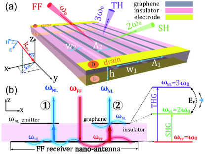
There are two key mechanisms that contribute to the remarkably large enhancement of the nonlinear optical response of the GIG structure, namely by several orders of magnitude as compared to that of a graphene sheet. The first one, indicated by path ① in Fig. 1(b), requires that the bottom GNR has a first-order plasmon at and a higher-order SPP at yywp17ptrsa . Then, the field at incident onto the bottom GNRs generates a strong field on these GNRs at , via the resonant excitation of first-order SPPs, and, subsequently, higher-order SPPs are resonantly generated by the nonlinear polarization in these same bottom GNRs.
We now introduce a new, much more efficient mechanism contributing to the enhancement of the nonlinear response of the GIG structure. It is schematically indicated by path ② in Fig. 1(b) and relies on the fact that the top GNRs possess first-order SPPs at the HH. This mechanism can be described as follows: the enhanced optical field due to the excitation of first-order SPPs on the bottom GNRs induces on the top GNRs a strong nonlinear polarization at the HH via near-field interaction. This, in turn, resonantly excites first-order SPPs on the top GNRs. Additionally, first-order SPPs on the top GNRs (at HH) are also directly generated via optical near-field coupling with higher-order SPPs of the bottom GNRs.
In the final stage of the nonlinear optical interaction between the incoming light and the GIG structure, the higher-order SPPs on the bottom GNRs and the first-order SPPs on the top GNRs couple to the radiative modes to generate a strong signal at the HH. In fact, this GIG system acts as a nonlinear Yagi-Uda nanoantenna nn11natpho : the bottom and top GNRs are the driver at and director at , respectively.
To illustrate these ideas, we considered a metasurface with the periods of the bottom and top graphene gratings of and , respectively. The widths and of the GNRs and the thickness, , of the spacer are designed so as to achieve a double-resonance effect. We assume that the spacer is made of polyethylene, which has relative permittivity of and is practically lossless at mid-infrared frequencies wam98ao . The linear and nonlinear optical responses of this GIG structure have been studied using an in-house developed code based on the GS-FDTD method; for details on the numerical approach see the Supplemental Material (SM) SM17GSFDTD .
In this method, the linear properties of graphene are modeled using a linear surface optical conductivity Hans08jap ,
| (1) |
Here, , , and are the Fermi energy, temperature, and relaxation time, respectively, , and .
The nonlinear optical response is described by nonlinear surface current densities determined by second- and third-order nonlinear surface susceptibilities cvs14newjphy ; csa16acsnano ; msa15njp ; dh09apl ; dh10prb ; gla11jlet ; mik11prb ; ard14prb . In the case of THG, the third-order surface current density of graphene is expressed as:
| (2) |
where is the frequency at the TH and is the third-order nonlinear surface optical susceptibility. It is described by a single scalar function, , via the relation cvs14newjphy ; csa16acsnano , with being the Kronecker delta. Furthermore, in the case of SHG arising from a local nonlinear polarization, the second-order nonlinear surface current density can be written as:
| (3) |
where is the frequency at the SH and is the second-order nonlinear surface optical susceptibility. Symmetry considerations based on the fact that graphene belongs to the symmetry group lead to the conclusion that the tensor has three independent nonzero components, , , and , where the symbols and refer to the directions perpendicular onto and parallel to the plane of graphene, respectively. The values of these parameters used in this study are , , and dh10prb ; ard14prb . Note that, as demonstrated in the SM, the qualitative conclusions of our study do not change if instead of a local second-order nonlinear response of graphene one considers a nonlocal one.
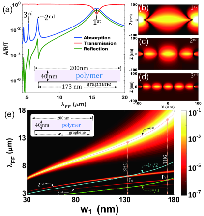
To characterize the linear optical response of the GIG structure, we first calculated the absorption, , transmittance, , and reflectance, , corresponding to the bottom graphene grating with geometrical parameters given in the inset of Fig. 2(a), and with , , and . The results of these calculations are summarized in Fig. 2(a). It can be seen that the absorption spectrum possesses a series of resonances, which are due to the excitation of SPPs on the GNRs. The field distributions of the first three SPPs are given in Figs. 2(b)-2(d), respectively. They show that the local optical field is strongly enhanced and confined around GNRs, with the largest field enhancement observed for the first-order SPP. Moreover, the results presented in Fig. 2(a) show that the absorption and reflectance spectra have resonances at the same wavelengths, a feature that is particularly useful for the optimization of the GIG structure.
A convenient procedure for designing a graphene grating in which a double-SPP-resonance phenomenon occurs is illustrated by the dispersion map of the absorption at the FF, presented in Fig. 2(e). The bands in this map, which show the width-dependent resonance wavelengths of SPPs of different order, suggest that it is possible to choose the width in such a way that a pair of SPPs exist at the FF and HH. Thus, if , a double resonance exists at the FF and SH, i.e. at (), with , whereas if , a double resonance exists at the FF and TH, i.e. at (), with .
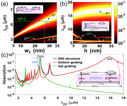
A drawback of the scheme we just described is that the plasmon at the HH is a higher-order plasmon and therefore it is less efficiently excited. In order to overcome this limitation and further enhance the nonlinear optical response of the device, another graphene grating is placed onto the spacer. The width of the GNRs of this top grating can be freely chosen. As such, it is chosen in such a way that at the HH (SH or TH) first-order plasmons exist in these GNRs. For example, as illustrated in Fig. 3(a), when the wavelength of the first-order plasmon of the GNRs of the top grating is equal to . Therefore, we expect that when , , and the GIG structure possesses first-order plasmons at both the FF and TH. This property is verified by the dispersion map of the absorption in the GIG structure, plotted in Fig. 3(b). This map shows that indeed the GIG structure has first-order plasmons at and , predominantly localized at the bottom and top gratings, respectively. Note that due to the optical coupling between the top and bottom gratings, the double resonance phenomenon in the decoupled bottom grating appears at a pair of wavelengths slightly blue-shifted as compared to those in the optimized GIG structure.
The optical coupling between the two gratings leads to several additional interesting phenomena, as per Fig. 3(b). First, the resonance wavelengths of SPPs vary with the thickness , especially at small values of for which there is a stronger coupling. Second, for , the resonance wavelengths of the first-order plasmon of the top grating and the third-order plasmon of the bottom grating are no longer equal, so that one expects a smaller enhancement of the THG. On the other hand, if is too large, the electric field at the FF in the bottom grating can no longer excite the first-order plasmon at the TH in the top grating, which also leads to decreased enhancement of the THG. Therefore, the optimum value of is . Note also that for , the second-order plasmon in the GIG structure is almost completely suppressed, a phenomenon explained by the fact that the system has a bound-state in the continuum for mbs08prl .
These conclusions are further validated by the absorption spectra presented in Fig. 3(c), where we compare the absorption in the bottom grating optimized to possess a double resonance at and , the absorption in the top grating designed to possess a fundamental plasmon at the TH wavelength, , and the absorption in the optimized GIG structure. These spectra show that by adding the top grating the absorption at the TH is enhanced by more than 12 times, which suggests that the local optical field and implicitly the nonlinear optical response of the GIG structure can be significantly enhanced.
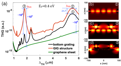
To quantify the enhancement of the THG in our GIG structure, we computed the THG spectra for a graphene sheet, the bottom grating optimized to possess a double resonance at and , and the optimized GIG structure, the results being compared in Fig. 4(a). These spectra show that, as compared to the graphene sheet, the THG in the optimized bottom grating is enhanced by when the FF coincides with that of the first-order plasmon of the bottom GNRs. Under the same excitation conditions, an additional enhancement is observed in the GIG structure. These results are explained by the spatial profiles of the amplitude of the dominant component of the TH electric field, , presented in Figs. 4(b) and 4(c). Thus, in the optimized bottom grating, at the TH, a third-order plasmon is excited, whereas in the optimized GIG structure both a first-order plasmon of the top grating and a third-order plasmon of the bottom grating are generated. Importantly, it can be seen that when the FF [ in Fig. 4(a)] is equal to that of the first-order plasmon of the top grating and the third-order plasmon of the bottom grating the THG is enhanced by , as compared to the case of a graphene sheet.
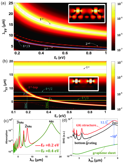
A particularly important property of the proposed GIG structure is the broadband nonlinearity enhancement at the HH, achievable by tuning the Fermi energy in the two gratings. The reason for this unique property is revealed by the dispersion map of the absorption of the optimized GIG structure, presented in Fig. 5(a). Thus, it is clear from this figure that the ratio between the wavelengths of the first-order SPP of bottom GNRs on the one hand, and third-order SPPs of the bottom GNRs and first-order SPPs of the top GNRs on the other hand, remains constant as the Fermi energy varies. Consequently, the double-resonance property is precisely preserved as the Fermi energy varies. More specifically, as shown in Fig. 5(a), when the Fermi energy is varied from , the resonance wavelength of the first-order plasmon of bottom GNRs, and implicitly the operating wavelength at the FF, varies from .
Another remarkable property of our proposed GIG structure is that it can enhance both the THG and SHG. Specifically, this functionality can be realized by tuning the Fermi energy only in the top grating, such that the resonance wavelength of first-order SPPs of the GNRs in this grating is shifted from the TH to the SH. This is demonstrated by the absorption map of the GIG structure presented in Fig. 5(b). Thus, this figure shows two types of plasmon bands, namely flat bands corresponding to SPPs in the bottom grating, which obviously do not depend on in the top grating, and plasmon bands associated to the top grating, whose resonance wavelength depends on . In particular, it can be seen that whereas the resonance wavelength on the first-order SPPs of the bottom grating remains constant, , the resonance wavelength of first-order SPPs of the top grating varies from to when is tuned from , respectively [see also Fig. 5(c)].
The strong enhancement of the SHG of the GIG structure, achieved for , is clearly demonstrated by the plots presented in Fig. 5(d), where we show the SHG spectra corresponding to a graphene sheet placed on the polymer substrate, the bottom grating, and the combined GIG structure, determined for for which the top GNRs have first-order SPPs at the SH. As in the case of the TH, one can see that strongly enhanced SHG can be achieved in the optimized GIG structure. In particular, at resonance, the SHG in the bottom grating is larger than in the case of a graphene sheet, whereas a further order of magnitude enhancement is achieved in the optimized GIG structure.
To conclude, a highly engineered GIG metasurface for enhancement of SH and TH is studied in this Letter. We demonstrate that it can be used to achieve tunable and dual-broadband enhancement of both nonlinear optical interactions, a property originating from the fact that our system possesses tunable double-resonances. In practice, this nonlinearity enhancement can be further improved by stacking several GIG units together to construct a 3D graphene metamaterial ylc12natnano . This new type of graphene structures could open up new research directions towards the development of novel ultra-compact and multi-frequency active photonic nanodevices.
Acknowledgements.
The authors acknowledge the use of UCL Legion High Performance Computing Facility (Legion@UCL), and associated support services, in the completion of this work. This work was supported by European Research Council (ERC), Grant Agreement no. ERC-2014-CoG-648328.References
- (1) K. S. Novoselov, A. K. Geim, S. V. Morozov, D. Jiang, Y. Zhang, S. V. Dubonos, I. V. Grigorieva, and A. A. Firsov, Science 306, 666 (2004).
- (2) C. Berger, Z. Song, X. Li, X. Wu, N. Brown, C. Naud, D. Mayou, T. Li, J. Hass, A. N. Marchenkov, and E. H. Conrad, Science 312, 1191 (2006).
- (3) A. K. Geim and K. S. Novoselov, Nat. Mater. 6, 183 (2007).
- (4) A. A. Balandin, S. Ghosh, W. Bao, T. Calizo, D. Teweldebrhan, F. Miao, and C. N. Lau, Nano Lett. 8, 902 (2008).
- (5) G. W. Hanson, J. Appl. Phys. 103, 064302 (2008).
- (6) A. H. Castro Neto, F. Guinea, N. M. R. Peres, K. S. Novoselov, A. K. Geim, Rev. Mod. Phys. 81, 109 (2009).
- (7) F. H. L. Koppens, D. E. Chang, and F. J. G. de Abajo, Nano Lett. 11, 3370 (2011).
- (8) J. Chen, M. Badioli, P. Alonso-Gonzalez, S. Thongrattanasiri, F. Huth1, J. Osmond, M. Spasenovic, A. Centeno, A. Pesquera, P. Godignon, A. Z. Elorza, N. Camara, F. J. G. de Abajo, R. Hillenbrand, and F. H. L. Koppens, Nature 487, 77 (2012).
- (9) Z. Fei, A. S. Rodin, G. O. Andreev, W. Bao, A. S. McLeod, M. Wagner, L. M. Zhang, Z. Zhao, M. Thiemens, G. Dominguez, and M. M. Fogler, A. H. Castro Neto, C. N. Lau, F. Keilmann, and D. N. Basov, Nature 487, 82 (2012).
- (10) A. N. Grigorenko, M. Polini, and K. S. Novoselov, Nat. Photon. 6, 749 (2012).
- (11) J. Chen, M. Badioli, P. Alonso-Gonzalez, S. Thongrattanasiri, F. Huth, J. Osmond, M. Spasenovic, A. Centeno, A. Pesquera, P. Godignon, and A. Z. Elorza, Nature 487, 77 (2012).
- (12) Y. V. Bludov, A. Ferreira, N. M. R. Peres, and M. I. Vasilevskiy, Int. J. Mod. Phys. B 27, 1341001 (2013).
- (13) F. J. G. de Abajo, ACS Photon. 1, 135 (2014).
- (14) M. Liu, X. Yin, E. Ulin-Avila, B. Geng, T. Zentgraf, L. Ju, F. Wang, X. Zhang, Nature 474, 64 (2011).
- (15) M. F. Craciun, S. Russo, M. Yamamoto, and S. Tarucha, Nano Today 6, 42 (2011).
- (16) V. W. Brar, M. S. Jang, M. Sherrott, J. J. Lopez, and H. A. Atwater, Nano Lett. 13, 2541 (2013).
- (17) C. R. Dean, A. F. Young, I. Meric, C. Lee, L. Wang, S. Sorgenfrei, K. Watanabe, T. Taniguchi, P. Kim, K. L. Shepard, and J. Hone, Nat. Nanotechnol. 5, 722 (2010).
- (18) T. Low and P. Avouris, ACS Nano 8, 1086 (2014).
- (19) Y. M. Lin, C. Dimitrakopoulos, K. A. Jenkins, D. B. Farmer, H. Y. Chiu, A. Grill, and P. Avouris, Science 327, 662 (2010).
- (20) F. Bonaccorso, Z. Sun, T. Hasan, and A. C. Ferrari, Nat. Photon. 4, 611 (2010).
- (21) Q. Bao and K. P. Loh, ACS Nano 6, 3677 (2012).
- (22) J. W. You, S. R. Bongu, Q. Bao, and N. C. Panoiu, Nanophotonics 8, 63 (2018).
- (23) N. Yousefi, X. Lu, M. Elimelech, and N. Tufenkji, Nat. Nanotechnol. 14, 107 (2019).
- (24) D. Jin, T. Christensen, M. Soljacic, N. X. Fang, L. Lu, and X. Zhang, Phys. Rev. Lett. 118, 245301 (2017).
- (25) D. Pan, R. Yu, H. Xu, and F. J. G. de Abajo, Nat. Commun. 8, 1243 (2017).
- (26) J. W. You, Z. Lan, Q. Bao, and N. C. Panoiu, IEEE J. Sel. Top. Quantum Electron. 26, (2020).
- (27) F. Xia, T. Mueller, Y. M. Lin, A. Valdes-Garcia, and P. Avouris, Nat. Nanotechnol. 4, 839 (2009).
- (28) F. Schedin, E. Lidorikis, A. Lombardo, V. G. Kravets, A. K. Geim, A. N. Grigorenko, K. S. Novoselov, and A. C. Ferrari, ACS Nano 4, 5617 (2010).
- (29) N. Papasimakis, Z. Luo, Z. X. Shen, F. de Angelis, E. di Fabrizio, A. E. Nikolaenko, and N. I. Zheludev, Opt. Express 18, 8353 (2010).
- (30) S. Kim, M. S. Jang, V. M. Brar, K. W. Mauser, L. Kim, and H. A. Atwater, Nano Lett. 8, 971 (2018).
- (31) H. Hu, X. Yang, X. Guo, K. Khaliji, S. R. Biswas, F. J. G. de Abajo, T. Low, Z. Sun, and Q. Dai, Nat. Commun. 10, 1131 (2019).
- (32) E. Hendry, P. J. Hale, J. Moger, A. K. Savchenko, and S. A. Mikhailov, Phys. Rev. Lett. 105, 097401 (2010).
- (33) S. Y. Hong, J. I. Dadap, N. Petrone, P. C. Yeh, J. Hone, and R. M. Osgood Jr, Phys. Rev. X 3, 021014 (2013).
- (34) J. L. Cheng, N. Vermeulen, and J. E. Sipe, New J. Phys. 16, 053014 (2014).
- (35) J. D. Cox, I. Silveiro, and F. J. G. de Abajo, ACS Nano 10, 1995 (2016).
- (36) D. A. Smirnova, A. V. Gorbach, I. V. Iorsh, I. V. Shadrivov, and Y. S. Kivshar, Phys. Rev. B 88, 045443 (2013).
- (37) M. A. Vincenti, D. de Ceglia, M. Grande, A. D. Orazio, and M. Scalora, Opt. Lett. 38, 3550 (2013).
- (38) M. Weismann and N. C. Panoiu, Phys. Rev. B 94, 035435 (2016).
- (39) J. W. You, J. You, M. Weismann, and N. C. Panoiu, Phil. Trans. R. Soc. A 375, 20160313 (2017).
- (40) G. Soavi, G. Wang, H. Rostami, D. G. Purdie, D. De Fazio, T. Ma, B. Luo, J. Wang, A. K. Ott, D. Yoon, S. A. Bourelle, J. E. Muench, I. Goykhman, S. Dal Conte, M. Celebrano, A. Tomadin, M. Polini, G. Cerullo, A. C. Ferrari, Nat. Nanotechnol. 13, 583 (2018).
- (41) J. W. You, Z. Lan, and N. C. Panoiu, Sci. Adv. 6, eaaz3910 (2020).
- (42) M. L. Nesterov, J. B. Abad, A. Y. Nikitin, F. J. G. Vidal, and L. M. Moreno, Laser Photon. Rev. 7, 7 (2013).
- (43) D. A. Smirnova, R. E. Noskov, L. A. Smirnov, and Y. S. Kivshar, Phys. Rev. B 91, 075409 (2015).
- (44) H. Deng, F. Ye, B. A. Malomed, X. Chen, and N. C. Panoiu, Phys. Rev. B 91, 201402 (2015).
- (45) H. Deng, X. Chen, B. A. Malomed, N. C. Panoiu, and F. Ye, Sci. Rep. 5, 15585 (2015).
- (46) D. Smirnova and Y. S. Kivshar, Phys. Rev. B 90, 165433 (2014).
- (47) M. T. Manzoni, I. Silveiro, F. J. G. Abajo, and D. E. Chang, New J. Phys. 17, 083031 (2015).
- (48) J. J. Dean and H. M. van Driel, Appl. Phys. Lett. 95, 261910 (2009).
- (49) J. J. Dean and H. M. van Driel, Phys. Rev. B 82, 125411 (2010).
- (50) M. Glazov, JETP Lett. 93, 366 (2011).
- (51) S. A. Mikhailov, Phys. Rev. B 84, 045432 (2011).
- (52) Y. Q. An, J. E. Rowe, D. B. Dougherty, J. U. Lee, and A. C. Diebold, Phys. Rev. B 89, 115310 (2014).
- (53) T. J. Constant, S. M. Hornett, D. E. Chang, and E. Hendry, Nat. Phys. 12, 124 (2016).
- (54) R. W. Boyd, Nonlinear Optics, 2nd ed., (Academic Press, New York, 2003).
- (55) H. Yan, X. Li, B. Chandra, G. Tulevski, Y. Wu, M. Freitag, W. Zhu, P. Avouris, and F. Xia, Nat. Nanotechnol. 7, 330 (2012).
- (56) I. V. Iorsh, I. S. Mukhin, I. V. Shadrivov, P. A Belov, and Y. S. Kivshar, Phys. Rev. B 87, 075416 (2013).
- (57) D. A. Smirnova, I. V. Shadrivov, A. I. Smirnov, and Y. S. Kivshar, Laser Photonics Rev. 8, 291 (2014).
- (58) L. Novotny and V. H. Niek, Nat. Photon. 5, 83 (2011).
- (59) Y. Wang, Y. Abe, Y. Matsuura, M. Miyagi, and H. Uyama, Appl. Opt. 37, 7091 (1998).
- (60) See Supplemental Material at [URL will be inserted by publisher] for details of the derivation and validation of GS-FDTD numerical method for simulation of linear and nonlinear optical properties of 2D materials.
- (61) G. W. Hanson, J. Appl. Phys. 103, 064302 (2008).
- (62) D. C. Marinica, A. G. Borisov, and S. V. Shabanov, Phys. Rev. Lett. 100, 183902 (2008).