∎
e1Corresponding author: bycel@tut.by \thankstexte2e-mail: solovyov@mbnresearch.com
MBN Explorer atomistic simulations of 855 MeV electron propagation and radiation emission in oriented silicon bent crystal: theory versus experiment
Abstract
The method of relativistic molecular dynamics is applied for accurate computational modelling and numerical analysis of the channelling phenomena for 855 MeV electrons in bent oriented silicon (111) crystal. Special attention is devoted to the transition from the axial channelling regime to the planar one in the course of the crystal rotation with respect to the incident beam. Distribution in the deflection angle of electrons and spectral distribution of the radiation emitted are analysed in detail. The results of calculations are compared with the experimental data collected at the MAinzer MIctrotron (MAMI) facility.
1 Introduction
The influence of a crystal structure on the passage of high-energy charged particles has been studied since the 1950s (see, for example, a collection of reviews in Ref. SaenzUberall1985 ). Nowadays, it is well-established that interaction of charged particles of high energies with crystals depends strongly on the crystal orientation.
At some crystal orientation the atoms arranged either in strings (axes) or in planes create a periodic electrostatic potential which acts on a projectile. If the incident angle of the projectile’s momentum with respect to an axis (or a plane) is small enough then the motion of the high-energy projectile is governed not by scattering from individual atoms but rather by a correlated action of many atomic centres of the electrostatic field. As a result, the projectile experiences a guided motion along the axial (or planar) direction. For positively charged projectiles the electrostatic field is repulsive at small distances so that they are steered into the inter-atomic region, while negatively charged projectiles move in the close vicinity of atomic strings or planes.
A phenomenon of a guided motion of charged particles in oriented crystals is called channelling111Channelling effect can be discussed not only for crystals but, in principle, for any structured material which provides “passages”, moving inside which a projectile has much lower value of the mean square of the multiple scattering angle than when moving along any random direction. The examples of such materials are nanotubes and fullerites, for which the channelling motion has been also investigated, see, e.g., Refs. ArtruEtAl_PhysRep2005 ; BellucciEtAl2003a ; Borka_Nanotube_2011 ; GreenenkoShulga2002 ; GevorgyanIspirian1997 ; ZhevagoGlebov2002 ; ZhevagoGlebov1998 ; Dedkov1998 . Lindhard’s comprehensive theoretical study Lindhard has demonstrated that the propagation of charged particles through a crystal strongly depends on the relative orientation to the crystal axes and planes. The important model of continuum potential for the interaction of energetic projectiles and lattice atoms was formulated.
Basing on this model it has been demonstrated that a projectile experiences the channelling motion if its transverse energy does not exceed the depth of the axial or interplanar electrostatic potential well. This condition can be formulated in terms of the angle between the particle’s velocity and the axial or planar direction Lindhard . Namely, must not exceed the maximum (critical) value given by
| (1) |
where is the projectile momentum with being the relativistic Lorentz factor. For an ultra-relativistic projectile one can substitute the product with the energy .
Channeling of charged particles is accompanied by the emission of Channelling Radiation (ChR) Kumakhov1976 . This specific type of electromagnetic radiation arises due to the oscillatory transverse motion of the projectile (so-called, channelling oscillations). The (quasi-)periodicity of the particle’s trajectory leads to the enhancement of the spectral intensity of radiation at frequencies (here stands for the frequency of channelling oscillations). In this frequency range, the intensity of ChR greatly exceeds (by more than an order of magnitude) that emitted by the same projectile in an amorphous medium (see, e.g., Uggerhoj1980 ).
As for now, a number of theoretical and experimental studies of the channelling phenomena (the motion and the radiation emission) in oriented crystals have been carried out (see, e.g., a review UggerhojRPM ).
The channelling phenomena occur in both straight and bent crystals. In the latter case, a channelling particle experiences the action of a centrifugal force (where is the bending radius) Tsyganov1976 in addition to that of the crystalline field. A stable channelling motion is possible if is less than the maximum transverse force due to the crystalline field. This leads to the restriction on the allowed values of the bending radius, . Since its prediction Tsyganov1976 and experimental confirmation ElishevEtAl:PLB_v88_p387_1979 , the idea of deflecting high-energy beams of charged particles by means bent crystals has attracted a lot of attention UggerhojRPM ; BiryukovChesnokovKotovBook . The experiments have been carried out with ultra-relativistic protons, ions, positrons, electrons, -mesons Scandale_etal:PL_B719_p70_2013 ; ScandaleEtAl:PRSTAB_v11_063501_2008 ; ScandaleEtAl:PRA_v79_012903_2009 ; Bandiera_etal:PRL_v115_025504_2015 ; Mazzolari_etal:PRL_v112_135503_2014 .

a)
b)
In panel a) the beam enters the crystal along the tangent to the crystal planes. The angular distribution of the initially over-barrier electrons at the entrance, label "1", is centered along the OZ direction, . The electrons captured into the channelling mode at the entrance follow the crystal bending and thus are deflected by larger angles. Some of these electrons, which channel through a part of the crystal and then dechannel (label "2"), contribute to the central part of the angular distribution. Those particles that channel through the whole crystal of length (label "3") contribute to the maximum of the distribution at .
Panel b) corresponds to the case when the angle between the incident beam and the tangent exceeds the Lindhard angle. As a result, most of the particles propagate in the over-barrier mode starting from the entrance. In this case, due to the crystal bending a particle can experience a volume reflection or a volume capture as marked by circles in the trajectories 1 and 2, respectively. The angular distribution of electrons provides the quantitative description of these events.
Experimentally, it is more advantageous to study the interaction of charged particles with a bent crystal rather than with a straight one. The former case provides the opportunity to analyze the channelling efficiency by separating the channelling particles from the over-barrier particles, i.e. those which travel across the crystal planes (axes) at the angle larger than the Lindhard critical angle.
Figure 1 a) shows a sketch of the experimental set-up which can be used to study the channelling efficiency by measuring the deflection angle of the incoming particles (electrons) due to the interaction with a bent crystal. The direction of the incident electron beam is aligned with the tangent to the crystal planes at the crystal entrance. Placing a detector behind the crystal one can measure the distribution of electrons with respect to the deflection angle . Different modes of the electrons motion contribute to different parts of the angular distribution (shown with a thick solid curve on the top of the panel). Namely, the distribution of the electrons that move in the over-barrier mode from the entrance to the exit points (see schematic trajectory 1) is centered along the OZ direction, i.e. at . The particles that channel through the whole crystal of length (trajectory 3) give rise to the maximum centered around (marked as ). Comparing the areas below these two maxima one can quantify the channelling efficiency, i.e. the relative number of the particles channelled through the whole crystal. Finally, the electrons captured into the channelling mode at the entrance but dechannelled somewhere inside the crystal (trajectory 2) experience deflection by the angle within the interval . Their angular distribution (curve ) allows one to deduce the dechannelling length of the particles.
By means of bent crystals one can study other phenomena associated with the interaction of charged particles with oriented crystalline medium, such as volume reflection (VR) and volume capture (VC) Taratin1987 . In this case, the incident beam is directed at an angle larger than the Lindhard angle, Figure 1b). As a result, at the crystal entrance most of the particles start moving in the over-barrier mode across the bent channels. As a result of the bending of the crystal, at some point in the crystal volume the incident angle with respect to the local tangent direction can become less than the Lindhard angle so that the particle enters the channelling mode. This effect known as VC is illustrated by trajectory 2. In the process of VR the over-barrier particle is deflected to the side opposite to the bend (see illustrative trajectory 1) being reflected from the potential barrier increased due to the centrifugal term where stands for the transverse coordinate. The efficiency of the VC and VR events in bent crystals can also be analyzed by measuring experimentally (or simulating numerically) the angular distribution of electrons behind the crystalline target.
Various approximations have been used to simulate channelling and other related phenomena in oriented crystals. Whilst, formally, most rigorous description can be achieved within the framework of quantum mechanics (see, e.g., Klenner_EtAl-PRA_v50_p1019_1994 ; PhysRevE.53.1129 ; BogdanovEtAl_JPhysCS_v236_012029_2010 ; WistisenPiazza_PRD_v99_116010_2019 and references therein), it has been shown AndersenEtAl_KDanVidensk_v39_p1_1977 that classical description in terms of particles trajectories provides highly adequate and accurate description in the limit when the number of quantum states of the transverse motion of a channelling particle is large enough. For light charged particles (electrons and positrons) the strong inequality becomes well fulfilled for the projectile energy in the hundred MeV range and above.
A direct approach to simulate a trajectory of a particle in a crystalline media is based on integration of the relativistic equations of motion in an external electric field :
| (2) |
where is the charge of the particle and .
Within the framework of continuum potential Lindhard , stands for the electric field due to atomic planes or strings so that the solution of (2) provides one- (planar channelling) or two-dimensional (axial channelling) trajectories, correspondingly. However, this approach becomes less applicable if the incident angle of the projectile with respect to the chosen plane (or axis) greatly exceeds several Lindhard’s critical angles . (More detailed analysis of the applicability of the continuum potential model may be found in Ref. Lindhard ). This scheme has been implemented in a number of codes BogdanovEtAl_JPhysCS_v236_012029_2010 ; BagliGuidi_NIMB_v309_p124_2013 ; Sytov_PR_AB_v22_064601_2019 ; XAVIER1990278 ; SytovTikhomirov_NIMB_v355_p383_2015 ; Dechan01 ; Nielsen_arXiv2019 ; Bandiera_Strong_Reduction_PRL_2018 . Some of these codes allow to account for the effects, which are beyond the continuous potential model by including a stochastic force due to the random scattering of the projectile by lattice electrons and nuclei Sytov_PR_AB_v22_064601_2019 ; SytovTikhomirov_NIMB_v355_p383_2015 ; Dechan01 ; Nielsen_arXiv2019 ; BaryshevskyTikhomirov_NIMB_v309_p30_2013 ; Tikhomirov_arXiv2015 and radiative damping force Dechan01 ; Nielsen_arXiv2019 ; Di_Piazza_2017 .
A Monte Carlo code described in KKSG_simulation_straight did not use the continuous potential to simulate the electron and positron channelling. Instead, it utilized the algorithm of binary collisions of the projectile with the crystal constituents basing on a peculiar model of the elastic scattering of a projectile from the crystal atoms in which atomic electrons are treated as point-like charges placed at fixed but random positions around the nucleus. The interaction of a projectile with each atomic constituent, electrons included, is treated as the classical Rutherford scattering from a static infinitely massive point charge. The applicability of this model has been argued MBN_ChannelingPaper_2013 ; ChannelingBook2014 ; Reply2018 .
The process of the radiation emission by an ultra-relativistic projectile can be treated in terms of classical electrodynamics (see, e.g., Jackson ) provided the photon energy is small compared to that of a projectile, . In this limit, one can neglect the effect of radiative recoil, i.e. the change in the projectile energy due to emission of quanta. The quasi-classical method is remarkable. It allows one to combine the classical description of the particle motion in an external field and the quantum effect of radiative recoil, due to Baier and Katkov method Baier_Katkov_1998_Singapore .
Within the framework of the quasi-classical method the radiative recoil is accounted for making possible correct calculation of the spectral-angular distribution of the radiation in the whole photon energy range with exception for the extreme high-energy tail of the spectrum, . Quasi-classical computation of the emission spectrum is implemented in a number of aforementioned codes or their extensions Dechan01 ; ChannelingBook2014 ; BandieraEtAl_NIMB_v355_p44_2015 ; Sytov_PR_AB_v22_064601_2019 ; Nielsen_arXiv2019 ; Bandiera_Strong_Reduction_PRL_2018 .
An approach based on molecular dynamics has been developed recently to describe the motion of relativistic projectiles in a crystalline environment. Three-dimensional simulations of the propagation of ultra-relativistic projectiles through the crystal can be performed using the MBN Explorer package MBN_Explorer_Paper ; MBNExplorer_Book ; MBN_cite . The package was originally developed as a universal computer program to allow investigation of structure and dynamics of molecular systems of different origin on spatial scales ranging from the atomic up to the mesoscopic ones. The general and universal design of the MBN Explorer code made it possible to expand its basic functionality with the introduction of a module that treats classical relativistic equations of motion (2) and generates the crystalline environment dynamically in the course of particle propagation MBN_ChannelingPaper_2013 . In course of the integration, the interaction of the projectiles with the crystalline environment is computed as a multi-center interaction with all those atoms that influence the motion. The relevant details can be found in the cited paper and in Ref. ChannelingBook2014 . Here we would like to stress that, the above approach treats the forces experienced by the projectiles in a much more accurate way than the commonly employed one based on the continuous potential concept. Using this software in combination with advanced computational facilities it is possible to simulate significant number of the trajectories for further analysis. For the trajectories generated, the software allows to calculate the spectral and angular distribution of the radiation emitted using the quasi-classical formalism.
A number of simulations have been performed for electrons and positrons of the sub-GeV and GeV energies channeling in straight, bent and periodically bent silicon, diamond and tungsten crystals SUSHKOJ.Phys2013 ; SushkoEaAl:JPConfSer-v438-012018-2013 ; PolozkovPhys.J.D2014 ; Korol2017 ; SHEN201826 ; ChannelingBook2014 ; BezchastnovKorolSolovyov2014 ; Pavlov-EtAl:JPB_v52_11LT01_2019 ; Pavlov-EtAl:EPJD_v74_21_2020 including comparison and benchmarking against experimental data MBN_ChannelingPaper_2013 ; Sushko_EtAl_NIMB_v355_p39_2015 ; BezchastnovKorolSolovyov2014 ; Backe_JINST_v13_C02046_2018 ; BackeEtAl_JINST_v13_C04022_2018 .
In this paper the numerical results obtained by means of the MBN Explorer software package are compared with the experimental data collected at MAinzer MIcrotron (MAMI) and reported in Refs. Mazzolari_etal:PRL_v112_135503_2014 ; Bandiera_etal:PRL_v115_025504_2015 .
2 Experimental setup

Experimental setup used to measure the radiation emission spectra and the distribution of electrons with respect to the deflection angle after passing through an oriented bent silicon crystal is schematically shown in Fig. 2. A 855 MeV electron beam, generated by the microtron, is aligned to the crystal mounted on a high-precision goniometer with three degrees of freedom, which allowed for a precise rotation of the target Backe-EtAl_NIMB_v266_p3835_2008 . Beyond the target, the electrons, deflected by magnets, move towards a luminosity screen (a detector). Hitting the screen an electron causes an optical flash that is detected by a photocamera. The angular distribution of electrons is built based on the processing of the detected flashes. An ionization chamber, indicated in the figure, allows one to measure electrons deflection intensity from the crystallographic axes and/or planes by scanning for different rotation angles. Before the main experiment the initial crystallographic directions were determined by means of a high resolution X-ray diffraction guidi_2009 . The ionization chamber was used for further tuning of the sample crystallographic directions with respect to the incident beam. More details on this procedure can be found in Refs. Backe-EtAl_NIMB_v266_p3835_2008 ; Backe_EtAl_JPhysConfSer_v438_012017_2013 .
The radiation emitted in the target is registered by an electromagnetic calorimeter located behind the crystal along the incident beam direction. To decrease the background radiation the calorimeter is placed behind a lead protection which has a mm hole to collimate the photon beam from the target. The hole size corresponds to the aperture of mrad.
2.1 Beam parameters
The MAMI facility provides continuous electron beam the energy of which can be varied from 195 up to 1600 MeV. In the experiments Mazzolari_etal:PRL_v112_135503_2014 ; Bandiera_etal:PRL_v115_025504_2015 the electrons were accelerated to 855 MeV. The beam spot experiments had standard deviations m, horizontally, and m, vertically, which were significantly smaller than the size of the crystal. The corresponding standard deviations of the beam divergences of and rad, are much smaller than Lindhard’s critical angle mrad for a 855 MeV electron the Si(111) planar channel.
2.2 The crystal used in the experiment
In the experiment, a bent silicon single crystal of thickness 30.5 m along the beam direction was used as a target. The crystal samples were fabricated at the Sensors and Semiconductor Laboratory (University of Ferrara) with the crystallographic orientation chosen to produce quasi-mosaic bending of the (111) plane guidi_2009 .222The quasi-mosaic effect consists in the bending of a family of lattice planes that are perpendicular to the surface of the primary curvature Ivanov-EtAl:JETP-Lett_v81_p99_2005 . Crystal thickness along the beam was 30.5 m and its bending radius was 33.5 mm, which is approximately 23 times larger than the critical radius for channeling at this energy Bandiera_etal:PRL_v115_025504_2015 . A thorough discussion of the processes behind quasi-mosaic bending as well as the details of the technological implementations can be found in Refs. Ricardo_Camattari_JAC_v489_p977_2015 ; guidi_2009 ; Mazzolari-EtAl:EPJC_v78_720_2018 .
2.3 Crystal orientation
In the experiment, the crystal was first oriented by aligning the crystalline axis 112 with the incident electron beam. Then, the crystal was rotated around the 111 axis to the position in which the beam is directed along the crystal plane . The choice of the (111) planes is due to the fact that they are the most effective ones for reflecting negatively charged particles.
3 Case studies
In our simulations we used a bent crystal with the parameters (thickness, bending radius) close to those used in the experiments. The simulations were carried out for a 855 MeV electron beam targeting the crystal at the directions corresponding to those probed experimentally as well as at directions that were not explored. It has allowed us to compare the simulated dependences with the experimentally measured data and to study the evolution of the angular distributions of deflected electrons and of the emission spectra with the variation in the relative orientation of the crystal and the beam.
In what follows we analyze in detail the transition from the axial to the planar mode and compare the results with available experimental data presented in Refs. Mazzolari_etal:PRL_v112_135503_2014 ; Bandiera_etal:PRL_v115_025504_2015 .
The atomistic approach implemented in MBN Explorer allows one to simulate the trajectories of charged particles entering a crystal along an arbitrary direction. We take this advantage and study the transition from electron capture by the crystalline axis 112 to the planar channelling mode in the bent (111) plane at different rotation angles. The crystal was oriented from the 112 axis along the beam direction to the channelling position in the (111) plane.
3.1 Crystal orientation used in the case studies
Let us describe the geometries of the beam-crystal orientation which were used in the case studies.

The first case study refers to the analysis of the change in the channelling properties in the course of transition from the axial to the planar channelling regime. Figure 3 illustrates the beam-crystal orientation in this case. The -axis is directed along the crystallographic axis which is normal to the plane. The -axis is aligned with the crystallographic direction. At the entrance, the beam velocity , being tangent to the plane, is directed at the angle to the -axis. For given the uniform bending of the plane is assumed with constant bending radius mm lying in the plane.
| axis | , rad |
|---|---|
| 0 | |
| 0.190126 | |
| 0.281035 | |
| 0.333473 | |
| 0.367422 | |
| 0.391144 | |
| 0.408638 | |
| 0.422064 |
The case corresponds to the axial channelling along the axis. Transition to the planar channelling regime can be realized by increasing the values of . In our simulations this has been implemented by means of the following two routines.
Firstly, to move away from the axial channelling along we have considered the values of corresponding to the axes with higher Miller indices such as , , …, up to . The limit corresponds to the planar channelling regime. The data presented in Table 1 indicates that for all considered the corresponding values of are in the range of hundreds of mrad.
Another option to monitor the transition from the axial channelling to the planar is by considering the values of within the range where to be chosen much larger than Lindhard’s critical angle, mrad, for the axis but much smaller than rad, see Table 1.
We note that the experimental data presented in Refs. Mazzolari_etal:PRL_v112_135503_2014 ; Bandiera_etal:PRL_v115_025504_2015 refer, as stated, to the planar channelling regime. However, the corresponding value of is not quoted.

The second case study, the geometry of which is illustrated by Figure 4, was devoted to the analysis of the volume reflection and volume capture phenomena. Here, the direction of the incident beam is characterized by two angles: defined as above, and the angle between and the plane. Bending of the plane is assumed with bending radius within the plane.
To match the experimental conditions indicated in Refs. Mazzolari_etal:PRL_v112_135503_2014 ; Bandiera_etal:PRL_v115_025504_2015 , we set mrad in the simulations. The angle was varied from to mrad.
4 Input parameters for simulation
The simulations have been performed by means of the MBN Explorer package MBN_cite , which supports a number of physical models including, in particular, the atomistic approach based on the relativistic molecular dynamics to simulate channelling of charged particles in crystals MBN_ChannelingPaper_2013 . The work with MBN Explorer is facilitated by a multitask software toolkit, MBN Studio MBN_Studio , which provides tools for designing crystalline systems, preparing the input data for simulation, setting up calculations, monitoring their progress and examining the results.
The electrons with energy 855 MeV were used as a source of initial particles for the simulation. As mentioned above, the angular divergence, and , of the beam at MAMI is much smaller than Lindhard’s angle. Therefore, in the main set of simulations the beam divergence was not accounted for, i.e. we used .
The beam dimensions are significantly larger than the size of the unit cell of the crystal, therefore, at the crystal entrance the uniform spatial distribution of the beam particles was assumed.
In the course of simulations, the crystal structure is generated dynamically following the propagation of the particle. In a bent crystal, the code modifies coordinates of the nodes in newly generated unit cells accounting for the finite value of the bending radius . In the simulations, we used mm and the crystal thickness was set to 30.5 m. as quoted in Ref. Mazzolari_etal:PRL_v112_135503_2014 .
5 Simulation of the electrons angular distribution
The modification of the particle angular distributions behind the bent crystal (see Figure 1) due to the change in the beam-crystal orientation can be studied at the atomistic level of detail by means of MBN Explorer. In this paper we analyse this modification during the transition from the axial to the planar channelling regimes by changing the rotation angle , see Figure 3. In the simulations, was varied over the broad interval, rad. This interval includes, in particular, the value mrad, for which we present a comparison of the simulation results with the experimental data.
5.1 Angular distribution in the case of axial channelling
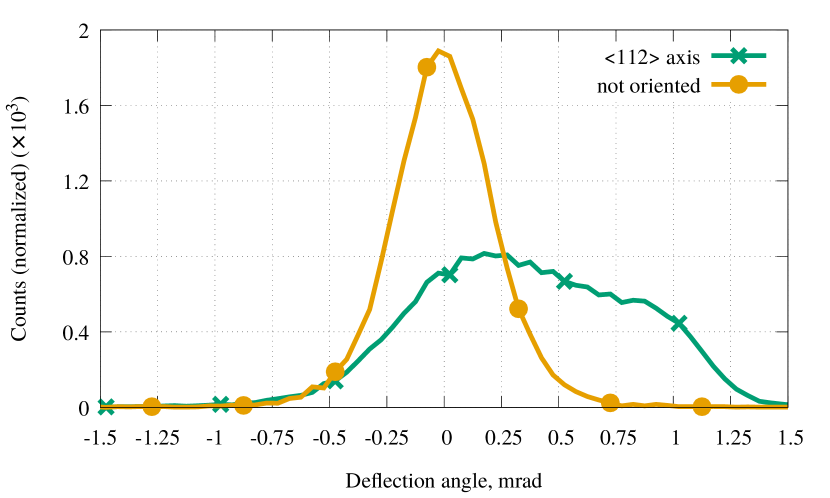
Setting one directs the incident beam along the axis. This geometry corresponds to axial channelling. The resulting distribution of electrons with respect to the deflection angle is presented in Figure 5, green curve with crosses. The electrostatic field in the oriented crystal influences the motion of electrons forcing them to follow the (bent) axial direction. As a result, there is a strong asymmetry of the distribution with respect to the incident beam direction (this corresponds to the deflection angle equal to zero). This behaviour differs notably from a symmetric profile of the distribution obtained for non-oriented (amorphous) silicon, orange curve with filled circles.
5.2 Evolution of the angular distribution with
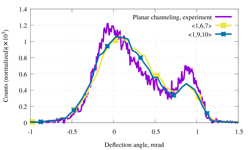
As mentioned in Sect. 3.1 above, one can increase by aligning the incident beam the axial directions along the plane. Gradual increase in the Miller index leads to the transformation of the electrostatic field acting on the projectile from the axial type to the planar one. As a result, one can monitor the change in the profile of the deflection angle distribution. Two panels in Figure 6 show the variation of electron angular distribution with respect to angles corresponding to several directions indicated in Table 1. For the sake of reference we also present the experimentally measured distribution, for which, however, the value of has not been clearly identified.
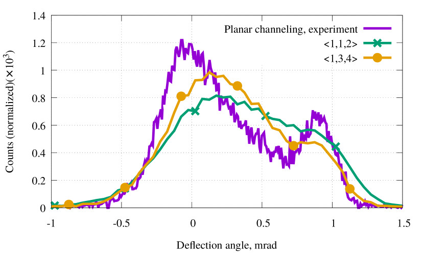
Intensity of the axial electrostatic field is the highest for the axial directions with small values of . In this case, the projectiles are captured, predominantly, into the axial channelling mode so that their distribution in the deflection angle is notably different from the planar case. This feature is illustrated by the upper panel in Figure 6 where the calculated distributions for channelling along 112 and 134 ( and 3, respectively) directions are compared with the experimentally observed one.
As increases, the axial field intensity decreases and the particle’s motion more and more acquires features of the planar channelling. In the simulations, it was noticed that starting with the angular distributions of electrons becomes virtually independent333This is valid for . For these values the angle between the and 011 axial directions, , is much smaller than Lindhard’s critical angle 0.55 mrad for the 011 axis, which is the limiting case for the direction as . on values of and the profile of the simulated distributions reproduces the features of the planar channelling seen in the experiment: the two maxima corresponding to the particles scattered at the entrance and to those which channel through the whole crystal, see lower panel in the figure. It is seen, however, that in all simulated distributions the first maximum is shifted towards positive values of the scattering angle whereas that in the experimental curve lies in the vicinity of the zero deflection angle being peaked at slightly negative values. Also to be noted is that the second maximum due to the channeling particles obtained in the simulations is lower than the experimentally measured one.
5.3 Evolution of angular distribution in the region of smaller angles
Another approach to simulate the planar channelling is to direct the incident beam along the plane at the angle (measured with respect to the 112 axis) that (i) is much less than 190 mrad, which corresponds to the nearest 123 axial direction, see Table 1, and (ii) is well above Lindhard’s critical angle mrad for a 855 MeV electron in case of axial channelling along 112.
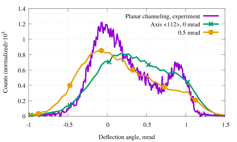
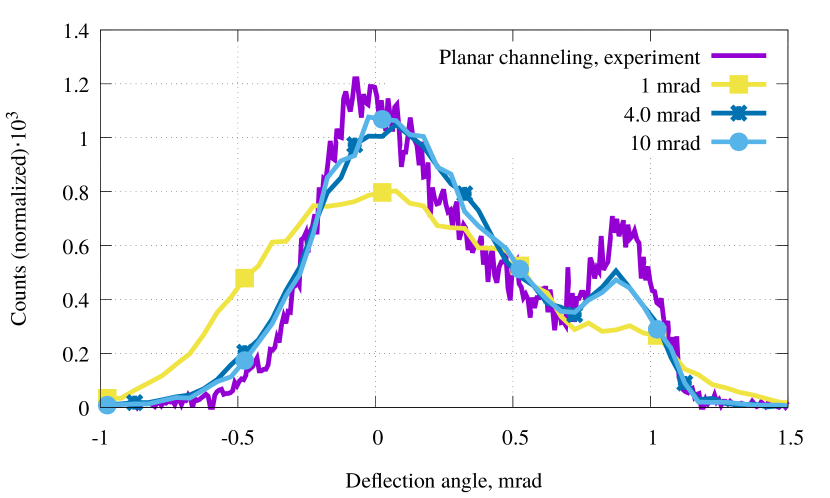
Figure 7 presents angular distributions calculated for several values of as indicated. In the upper panel, the distribution calculated for a small value mrad is shifted to the left from that obtained for the pure axial channelling (the curve ) and also exhibits strong deviations from the experimental data. For the incident angles within the interval mrad the shape of the simulated dependence experiences strong modifications but for mrad it stabilizes becoming close to that of the experimentally measured one, see the lower panel.
5.4 Scan over the rotation angle
To obtain a more detailed description on the dependence of the distribution of electrons in the deflection angle the simulations have been performed scanning over the two ranges of indicated in Sects. 5.2 and 5.3.
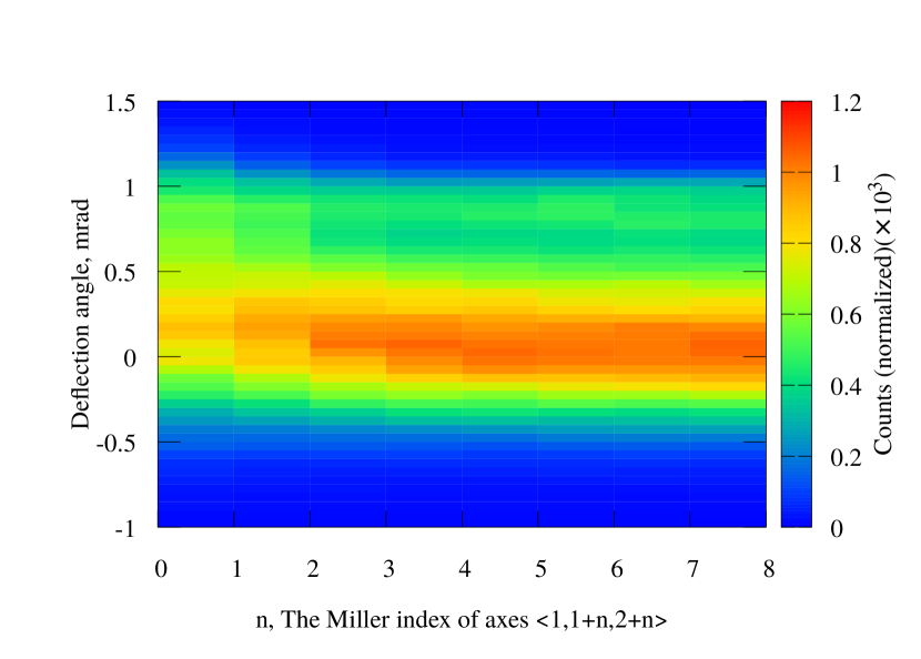
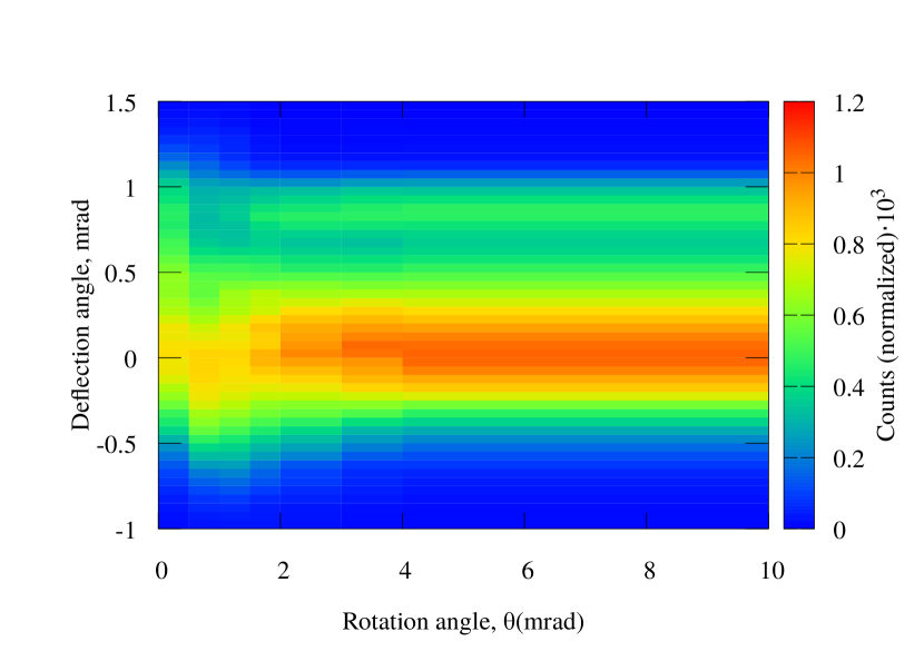
Upper panel in Figure 8 shows an angular scan over the region of large , which includes the axial directions with the Miller index ranging from 0 to 8. The plot has to be seen as a set of vertical stripes, each located between two neighbouring values of . Within each stripe, the colour mapping represents the same angular distribution that corresponds to equal to the angle between the axes and . The plot allows one to visualize, within the framework of a single figure, the evolution with of the angular distributions that are shown separately in Figures 5 and 6. The results presented indicate that the axial directions corresponding to can be equally used to simulate the planar channelling along the plane. Lower panel in the figure presents the scan over smaller values, i.e. much less that mrad, which corresponds to the angular direction. Here, the planar channelling can be adequately simulated in the region mrad where the angular distribution remains virtually unchanged.
5.5 Comparison with the experiment
The data presented in this section refer to the second case study, see Figure 4. The simulations were carried out using the parameters that match the experimental conditions Mazzolari_etal:PRL_v112_135503_2014 ; Bandiera_etal:PRL_v115_025504_2015 .
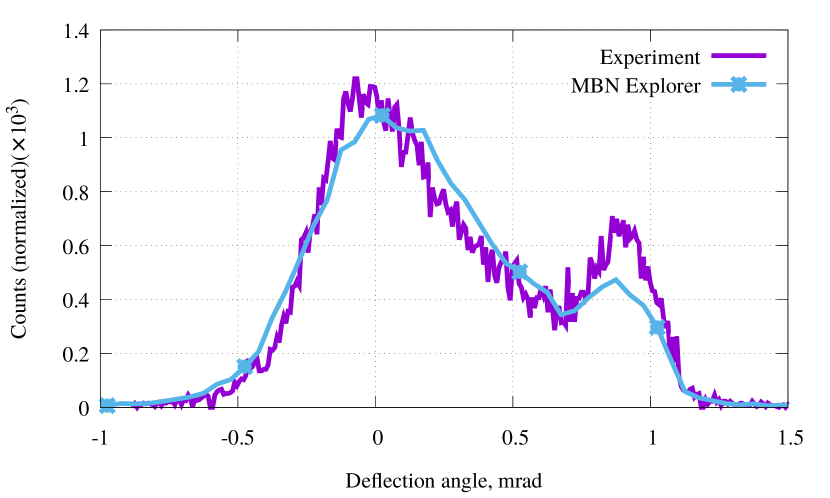
Figure 9 compares the results of simulation with the experimental data for the angular distribution of 855 MeV electrons incident along the plane () at the entrance of bent silicon crystal. On the whole, there is good agreement between theory and experiment but there are also some differences.
First, the maximum centered at zero deflection angle, which corresponds to the distribution of electrons that become over-barrier at the entrance, in the simulated curve is slightly shifted to the right as compared to the maximum in the experimentally measured dependence. In the course of simulations it has been noticed that the closest agreement in the maxima positions is achieved at the smaller incident angles mrad. In this range the simulated angular distribution does not virtually depend on the incident angle. In contrast to this, for the higher incident angles, corresponding to the axial directions with high indices , the deviation from the experiment is more pronounced. This feature indicates that although the field intensities of the high-index axes are weak they, nevertheless, influence the angular distribution of particles.
The second difference to be noted is that the peak, centered at the deflection angle about 0.8 mrad, in the simulated dependence is lower that its experimental counterpart. This peak is due to the electrons that channel through the whole length of a crystal. To make this peak pronounced the value of should be comparable with the dechannelling length . The simulations carried out in Ref. SushkoEaAl:JPConfSer-v438-012018-2013 by means of the MBN Explorer produced the result m for 855 MeV electrons channelled in oriented Si(111) crystal bent with radius mm. The crystal thickness along the beam m which is very close to the value 33.5 mm used in the experiments Mazzolari_etal:PRL_v112_135503_2014 ; Bandiera_etal:PRL_v115_025504_2015 was thin enough to observe the peak of channelled electrons.
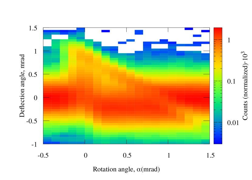
A set of simulations has been carried out aimed at studying modifications in the angular distributions of electrons after interaction with the crystal as a function of the incident angle . The results obtained are presented in Figure 10 which shows a scan over the rotation angle from to mrad. The pattern of the angular distribution is similar to that observed experimentally Mazzolari_etal:PRL_v112_135503_2014 .
5.6 Volume reflection: Simulation versus experiment
A set of simulations has been carried out aiming at a more detailed study of the impact of the volume reflection phenomenon on the angular distribution of electrons at the incident angle = 0.45 mrad. The second angle was set to 95 mrad.
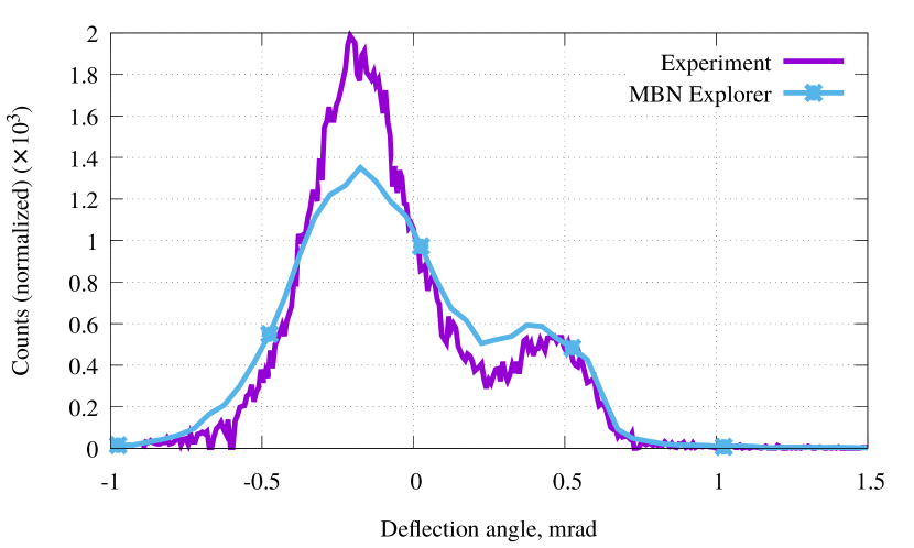
The simulated angular distribution is presented in Figure 11 together with the experimental data. In accordance with illustrative picture b) in Figure 1 and the corresponding qualitative explanation outlined in the caption, the main modification in the angular distribution, as compared to the case , is that the main maximum due to the over-barrier particles is shifted to the left. This is a direct consequence of the volume reflection events which occur in the crystal bulk. The second less powerful maximum seen at the deflection angle of about 0.5 mrad appears as a result of the volume capture events: the electrons are captured in the channelling mode at some point in the bulk where there velocity becomes aligned with the tangent of the bent plane Taratin1987 .
The dependences shown indicate that in the simulations the peak due to VC corresponds well to the experiment, whereas the peak associated with VR is lower and slightly wider than the experimentally measured one.
6 Radiation emission spectra
The transition from the axial to planar channelling regimes is revealed also in the changes in spectral distributions of the radiation emitted by projectiles.
Calculation of emission spectra is provided by a special module of MBN Explorer which uses pre-calculated trajectories as the input data. The spectral intensities of radiation presented below have been calculated from the same electron trajectories as used in analyzing the angular distributions.
6.1 Evolution of the emission spectra with the incident angle
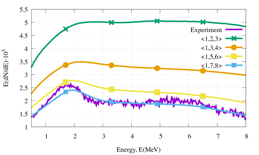
Figure 12 shows emission spectra calculated for 855 MeV electrons entering silicon crystal tangentially to its bent plane along several axial directions . These directions correspond to large values of the incident angles measured with respect to the axis, see Table 1. With increasing, the averaged axial electric field decreases leading to the decrease in the radiation intensity. At (the 178 axial direction) the spectrum approaches that emitted in the planar channelling regime and becomes virtually insensitive to further increase of .
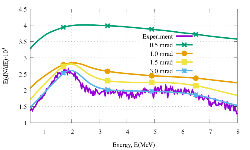
Similar modification of the spectra occurs when the incident angle varies within the interval mrad, see Figure 13. In this case, small values of correspond to the motion close to the axial direction where a projectile experiences action of the strong axial field and, thus, radiates intensively. As increases, a projectile moves across the axes experiencing smaller acceleration in the transverse direction. As a result, the intensity decreases (compare the curves corresponding to , 1.0 and 1.5 mrad). For much larger than the critical angle for the axial channelling, the spectrum approaches its limit, which corresponds to the planar channelling regime.
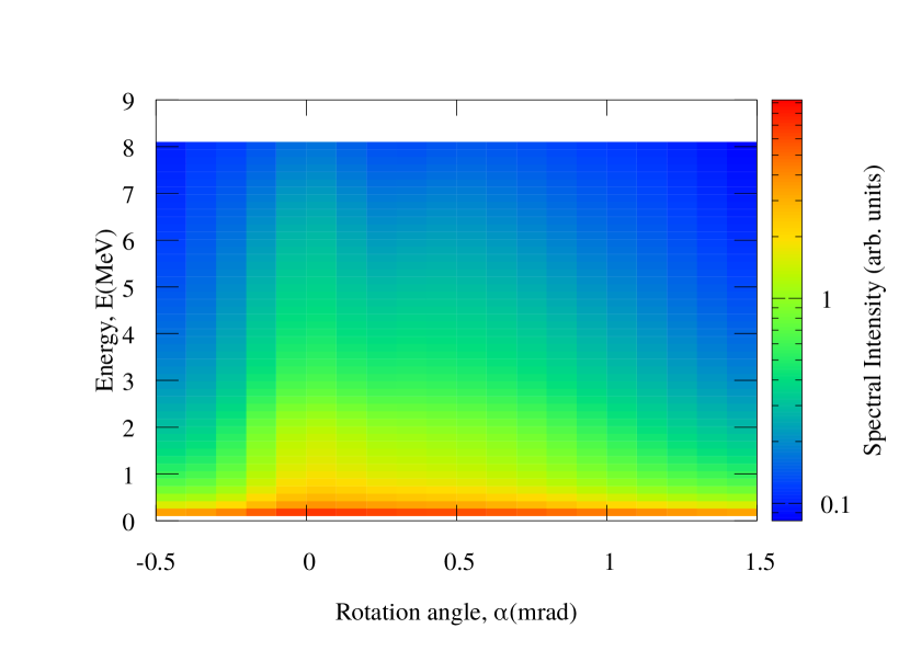
In Figure 14 the emission spectra presented in the form of a scan over angle varying within the interval from -0.5 to 1.5 mrad as in the experiment Bandiera_etal:PRL_v115_025504_2015 . On total, the colour map corresponds to that presented in Figure 1(b) of the cited paper. However, to carry out a more detailed comparison, below we consider emission spectra at certain geometries.
6.2 Comparison with the experiment
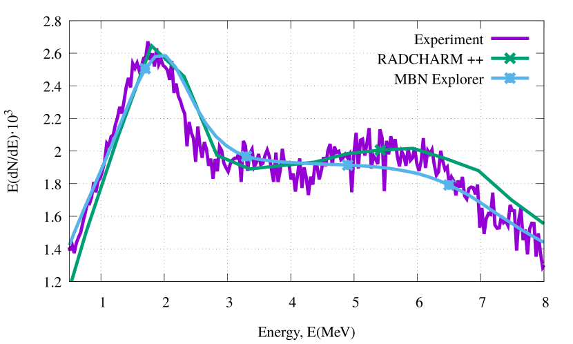
For angles mrad and (the channelling regime), a comparison of the spectra obtained in the simulations with those measured experimentally is presented in Figure 15. The dependence calculated by means of the RADCHARM code BandieraEtAl_NIMB_v355_p44_2015 is presented as well. 444This code utilizes the continuous potential to describe the channeling motion and the Baier and Katkov method to calculate the spectral distribution of radiation.
In Ref. Bandiera_etal:PRL_v115_025504_2015 the spectral distributions are presented in arbitrary units whereas the current simulations produced the absolute values. Therefore, to compare the simulated results with the experimental ones the simulated data were re-scaled to produce the same area as in the experiment. This procedure, carried out for the spectra emitted in the channelling regime, provided the normalization factor which has been used to re-scale the spectra simulated in the geometry corresponding to the VR regime. Comparing the curves presented in Figure 15 we state that the results obtained for the planar channelling regime there is a good agreement between experiment and theory.
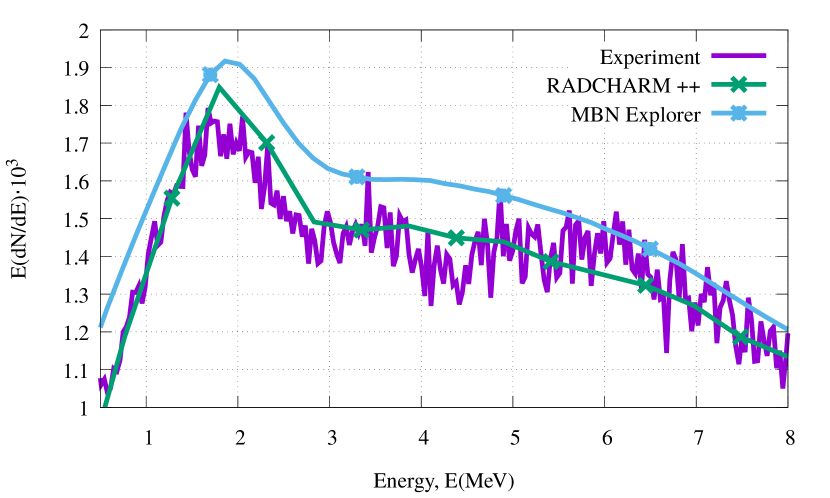
For the geometry, which allows for the VR and VC regime, a comparison of the simulation results and experimental data is shown in Figure 16. It is seen, that although the shapes of the simulated and measured spectra are the same, the absolute values differ by about 10 per cent (in the maximum). The difference of the intensities is related to that seen in the angular distribution of the electrons, Figure 11.
7 Conclusions
The atomistic approach implemented in MBN Explorer allowed us to monitor in detail the changes in the distribution of the deflected electrons and in the emission spectra that occur when the 855 MeV electron beam enters a thin bent oriented silicon crystal along different directions. In particular, we have revealed the ranges of the angle between the beam and the 112 axis which correspond to the planar channelling regime. To achieve the planar channelling one can direct the beam either along the axial directions with (this corresponds to large angles, rad) or to vary the angle within the interval mrad, i.e. where the upper boundary stands for the angle between the 112 and 123 axes.
Comparison of the results of simulation with the experimental data has been carried out for the two geometries of the beam-crystal orientation corresponding to (i) the channelling conditions, when the beam is aligned with the tangent to the planar direction at the entrance, and (ii) the volume reflection and volume capture regime. We may state that globally there is good agreement between theory and experiment. In case (i) and (ii) some the discrepancies have been revealed in the distribution of electrons. In the channelling regime the experiment goes slightly above the simulated curve in the vicinity of the channelling peak whereas in case (ii) more notable difference is seen for the peak associated with volume reflection. The emission spectrum simulated for the channelling regime agrees perfectly with the experimentally measured one. In case (ii) the simulated data exhibit approximately 10 per cent excess over the experiment.
Possible reasons for the discrepancies can be associated with (i) particular force field (the Moliére one) chosen to describe the electron-atom interaction in the course of simulations and (ii) effects not included into the simulations (e.g., quantum effects in multiple scattering in crystals Tikhomirov_PR_AB_v22_054501_2019 ; erratumTikhomirov_PR_AB_v22_054501_2019 ; arXivTikhomirov_PR_AB_v22_054501_2019 ; Artru2020QuantumVC ). We plan to clarify these issues in our future work.
Acknowledgements
We acknowledge support by the European Commission through the N-LIGHT Project within the H2020-MSCA-RISE-2019 call (GA 872196) and by Deutsche Forschungsgemeinschaft (Project No. 413220201). This work has been also partially supported through the CSN5-STORM experiment. A. Romagnoni acknowledges support from the ERC Consolidator Grant SELDOM G.A. 771642.
We acknowledge the CINECA award under the ISCRA initiative, for the availability of high performance computing resources and support.
References
- (1) A.W. Sáenz, H. Überall, Coherent Radiation Sources (Springer-Verlag Berlin Heidelberg, 1985)
- (2) X. Artru, S.P. Fomin, N.F. Shul’ga, K.A. Ispirian, N.K. Zhevago, Carbon nanotubes and fullerites in high-energy and X-ray physics. Phys. Rep. 412, 89-189 (2005)
- (3) S. Bellucci, V.M. Biryukov, Yu.A. Chesnokov, V. Guidi, W. Scandale, Channeling of high energy beams in nanotubes. Nucl. Instrum. Methods Phys. Res. B 202, 236-241 (2003)
- (4) D. Borka, S. Petrović, N. Nešković, Channeling of protons through carbon nanotubes. in Advances in Nanotechnology, ed. by Bartul, Z., Trenor, J., vol. 5, pp. 1–54 (Nova Science Publishers, Hauppauge, 2011)
- (5) A.A. Greenenko, N.F. Shul’ga, Passage of fast charged particles through bent crystals and nanotubes. Nucl. Instrum. Methods B 193, 133-138 (2002)
- (6) L.A. Gevorgyan, K.A. Ispirian, R.K. Ispirian, Channeling in single-wall nanotubes: possible applications. JETP Lett. 66, 322-326 (1997)
- (7) N.K. Zhevago, V.I. Glebov, Channeling of fast particles in fullerites. JETP 94, 1121-1133 (2002)
- (8) N.K. Zhevago, V.I. Glebov, Channeling of fast charged and neutral particles in nanotubes. Physics letters. A. 250, 360-368 (1998)
- (9) G.V. Dedkov, Fullerene nanotubes can be used when transporting gamma-quanta, neutrons, ion beams and radiation from relativistic particles. Nucl. Instrum. Methods B 143, 584-590 (1998)
- (10) J. Lindhard, Influence of crystal lattice on motion of energetic charged particles. K. Dan. Vidensk. Selsk. Mat. Fys. Medd. 34, 1 (1965)
- (11) M.A. Kumakhov, On the theory of electromagnetic radiation of charged particles in a crystal, Phys. Lett. A 51 17-18 (1976)
- (12) E. Uggerhøj, Channeling in the GeV-region. Nucl. Instrum. Method Phys. Res. 170, 105–113 (1980)
- (13) U. Uggerhøj, The interaction of relativistic particles with strong crystalline fields. Rev. Mod. Phys. 77, 1131 (2005)
- (14) E.N. Tsyganov, Fermilab Preprints TM-682: Some aspects of the mechanism of a charged particle penetration through a monocrystal. & TM-684: Estimates of Cooling and bending processes for charged particle penetration through a monocrystal. (Fermilab, Batavia, 1976)
- (15) A.F. Elishev et al., Steering of charged particle trajectories by a bent crystal. Phys. Lett. B 88, 387-391 (1979)
- (16) V.M. Biryukov, Yu.A. Chesnokov, V.I. Kotov. Crystal Channeling and its Application at High-Energy Accelerators. (Springer Science & Business Media, 2013)
- (17) W. Scandale et al., Measurement of the dechanneling length for high-energy negative pions. Phys. Lett. B 719, 70-73 (2013)
- (18) W. Scandale et al., Deflection of 400 GeV/c proton beam with bent silicon crystals at the CERN Super Proton Synchrotron. Phys. Rev. Accel. Beams 11, 063501 (2008)
- (19) W. Scandale et al., Experimental study of the radiation emitted by 180 GeV/c electrons and positrons volume-reflected in a bent crystal. Phys. Rev. A 79, 012903 (2009)
- (20) L. Bandiera et al., Investigation of the electromagnetic radiation emitted by sub-GeV electrons in a bent crystal. Phys. Rev. Lett. 115, 025504 (2015)
- (21) A. Mazzolari et al., Steering of a sub-GeV electron beam through planar channeling enhanced by rechanneling. Phys. Rev. Lett. 112, 135503 (2014)
- (22) A. Taratin, S. Vorobiev, "Volume reflection" of high-energy charged particles in quasi-channeling states in bent crystals, Phys. Lett. A 119, 425 (1987)
- (23) J. Klenner, J. Augustin, A. Schäfer, W. Greiner, Photon-photon interaction in axial channeling. Phys. Rev. A 50, 1019-1026 (1994)
- (24) A.V. Solov’yov, A. Schäfer, W. Greiner, Channeling process in a bent crystal. Phys. Rev. E 53, 1129-1137 (1996)
- (25) O.V. Bogdanov, E.I. Fiks, K.B. Korotchenko, Yu.L. Pivovarov, T.A. Tukhfatullin, Basic channeling with mathematica: a new computer code. J. Phys. Conf. Ser. 236, 012029 (2010)
- (26) T.N. Wistisen, A. Di Piazza, Complete treatment of single-photon emission in planar channeling. Phys. Rev. D 99, 116010 (2019)
- (27) J.U. Andersen, S.K. Andersen, W.M. Augustyniak, Channeling of electrons and positrons. K. Dan. Vidensk. Selsk. Mat. Fys. Medd. 39, 1-58 (1977)
- (28) X. Artru , A simulation code for channeling radiation by ultrarelativistic electrons or positrons, Nucl. Instrum. Methods B 48, 278-282 (1990)
- (29) E. Bagli, V. Guidi, Dynecharm++: a toolkit to simulate coherent interactions of high-energy charged particles in complex structures, Nucl. Instrum. Methods B 309, 124-129 (2013)
- (30) A.I. Sytov, V.V. Tikhomirov, L. Bandiera, Simulation code for modeling of coherent effects of radiation generation in oriented crystals. Phys. Rev. Accel. Beams 22, 064601 (2019)
- (31) A. Sytov, V.V. Tikhomirov, CRYSTAL simulation code and modeling of coherent effects in a bent crystal at the LHC. Nucl. Instrum. Methods B 355, 383-386 (2015)
- (32) A.V. Korol, A.V. Solov’yov, W. Greiner, The influence of the dechannelling process on the photon emission by an ultra-relativistic positron channelling in a periodically bent crystal. J. Phys. G 27, 95-125 (2001)
- (33) C.F. Nielsen, GPU accelerated simulation of channeling radiation of relativistic particles. arXiv:1910.10391 [physics.comp-ph] (2019)
- (34) L. Bandiera et al., Strong Reduction of the Effective Radiation Length in an Axially Oriented Scintillator Crystal, Phys. Rev. Lett. 121, 021603 (2018)
- (35) V. G. Baryshevsky, V. V. Tikhomirov, Crystal undulators: from the prediction to the mature simulations. Nucl. Instrum. Methods B 309, 30-36 (2013)
- (36) V.V. Tikhomirov, A Benchmark Construction of Positron Crystal Undulator. arXiv:1502.06588 [physics.acc-ph] (2015)
- (37) A. Di Piazza, T.N. Wistisen, U. I. Uggerhøj, Investigation of classical radiation reaction with aligned crystals, Phys. Lett. B, 765, 1-5 (2017)
- (38) A. Kostyuk, A.V. Korol, A.V. Solov’yov, W. Greiner, Planar channeling of 855 MeV electrons in silicon: Monte Carlo simulations. J. Phys. B 44, 075208 (2011)
- (39) G.B. Sushko, V.G. Bezchastnov, I.A. Solov’yov, A.V. Korol, W. Greiner, A.V. Solov’yov, Simulation of ultra-relativistic electrons and positrons channeling in crystals with MBN Explorer. J. Comput. Phys. 252, 404-418 (2013)
- (40) A.V. Korol, A.V. Solov’yov, W. Greiner, Channeling and Radiation in Periodically Bent Crystals, Second ed., (Springer-Verlag, Berlin, Heidelberg, 2014)
- (41) V.G. Bezchastnov, A.V. Korol, A.V. Solov’yov, Reply to Comment on ’Radiation from multi-GeV electrons and positrons in periodically bent silicon crystal’. J. Phys. B At. Mol. Opt. Phys. 51, 168002 (2018)
- (42) J.D. Jackson, Classical Electrodynamics. (Wiley, Hoboken, 1999)
- (43) V.N. Baier, V.M. Katkov, V.M. Strakhovenko, Electromagnetic Processes at High Energies in Oriented Single Crystals(World Scientific, Singapore, 1998)
- (44) L. Bandiera, E. Bagli, V. Guidi, V.V. Tikhomirov, RADCHARM++: A C++ routine to compute the electromagnetic radiation generated by relativistic charged particles in crystals and complex structures, Nucl. Instrum. Methods Phys. Res. B 355, 44-48 (2015)
- (45) I.A. Solov’yov, A.V. Yakubovich, P.V. Nikolaev, I. Volkovets, A.V. Solov’yov, MesoBioNano Explorer - a universal program for multiscale computer simulations of complex molecular structure and dynamics. J. Comput. Chem. 33, 2412-39 (2012)
- (46) I.A. Solov’yov, A.V. Korol, A.V. Solov’yov, Multiscale Modeling of Complex Molecular Structure and Dynamics with MBN Explorer. (Springer International Publishing, Cham, Switzerland, 2017)
- (47) MBN Explorer and MBN Studio Software. https://mbnresearch.com Accessed 8 May 2020
- (48) G.B. Sushko, V.G. Bezchastnov, A.V. Korol, Walter Greiner, A. V.V Solov’yov, R.G. Polozkov, V.K. Ivanov, Simulations of electron channeling in bent silicon crystal. J. Phys. Conf. Ser. 438, 012019 (2013)
- (49) G.B. Sushko, A.V. Korol, Walter Greiner, A.V. Solov’yov, R.G. Polozkov, V.K. Ivanov, Sub-GeV Electron and Positron Channeling in Straight, Bent and Periodically Bent Silicon Crystals J. Phys. Conf. Ser. 438, 012019 (2013)
- (50) R.G. Polozkov, V.K. Ivanov, G.B. Sushko, A.V. Korol, A.V. Solov’yov, Radiation emission by electrons channeling in bent silicon crystals. Eur. Phys. J. D 68, 268 (2014)
- (51) A.V. Korol, V.G. Bezchastnov, A.V. Solov’yov, Channeling and radiation of the 855 MeV electrons enhanced by the re-channeling in a periodically bent diamond crystal. Eur. Phys. J. D 71, 174 (2017)
- (52) H. Shen, Q. Zhao, F.S. Zhang, G.B. Sushko, A.V. Korol, A.V. Solov’yov, Channeling and radiation of 855 MeV electrons and positrons in straight and bent tungsten (110) crystals. Nucl. Instrum. Methods Phys. Res. B 424, 26-36 (2018)
- (53) A.V. Pavlov, A.V. Korol, V.K. Ivanov, A.V. Solov’yov, Interplay and specific features of radiation mechanisms of electrons and positrons in crystalline undulators, J. Phys. B 52, 11LT01 (2019)
- (54) A.V. Pavlov, A.V. Korol, V.K. Ivanov, A.V. Solov’yov, Channeling of electrons and positrons in straight and periodically bent diamond(110) crystals, Eur. Phys. J. D 74, 21 (2020)
- (55) V.G. Bezchastnov, A.V. Korol, A.V. Solov’yov, Radiation from Multi-GeV Electrons and Positrons in Periodically Bent Silicon Crystal, J. Phys. B 47, 195401 (2014)
- (56) G.B. Sushko, A.V. Korol, A.V. Solov’yov, Multi-GeV electron and positron channeling in bent silicon crystals. Nucl. Instrum. Methods Phys. Res. B 355, 39-43 (2015)
- (57) H. Backe, Electron channeling experiments with bent silicon single crystals – a reanalysis based on a modified Fokker-Planck equation, J. Instrum. (JINST) 13, C02046 (2018)
- (58) H. Backe, W. Lauth, T.N. Tran Thi, Channeling experiments at planar diamond and silicon single crystals with electrons from the Mainz Microtron MAMI, J. Instrum. (JINST) 13, C04022 (2018)
- (59) H. Backe, P. Kunz, W. Lauth, A. Rueda, Planar channeling experiments with electrons at the 855 MeV Mainz Microtron MAMI. Nucl. Instrum. Methods B 266, 3835-3851 (2008)
- (60) H. Backe, D. Krambrich, W. Lauth, K.K. Andersen, J.L. Hansen, U.I. Uggerhøj, Channeling and Radiation of Electrons in Silicon Single Crystals and Si1-xGex Crystalline Undulators. J. Phys.: Conf. Ser. 438, 012017 (2013)
- (61) R. Camattari, V. Guidi, V. Bellucci, A. Mazzolari, The ’quasi-mosaic’ effect in crystals and its applications in modern physics. J. Appl. Crystallogr. 48, 977-989 (2015)
- (62) V. Guidi, A. Mazzolari, D. De Salvador, A. Carnera, Silicon crystal for channelling of negatively charged particles J. Phys. D: Appl. Phys. 42, 182005 (2009)
- (63) Yu. M Ivanov, A. A. Petrunin, and V. V. Skorobogatov, Observation of the elastic quasi-mosaicity effect in bent silicon single crystals. JETP Lett. 81, 99 (2005)
- (64) A. Mazzolari, M. Romagnoni, R. Camattari, E. Bagli, L. Bandiera, G. Germogli, V. Guidi, G. Cavoto, Bent crystals for efficient beam steering of multi TeV-particle beams. Eur. Phys. J. C 78, 720 (2018)
- (65) G.B. Sushko, I.A. Solov’yov, A.V. Solov’yov, Modeling MesoBioNano systems with MBN Studio made easy. J. Mol. Graph. Model. 88, 247-260 (2019)
- (66) V.V. Tikhomirov, Quantum features of high energy particle incoherent scattering in crystals. Phys. Rev. Accel. Beams 22, 054501 (2019)
- (67) V.V. Tikhomirov, Erratum: Quantum features of high energy particle incoherent scattering in crystals [Phys. Rev. Accel. Beams 22, 054501 (2019)]. Phys. Rev. Accel. Beams 23 039901 (2020) , DOI: 10.1103/PhysRevAccelBeams.23.039901
- (68) V.V. Tikhomirov, Relativistic particle incoherent scattering in oriented crystals. arXiv:2004.06020v1 [physics.acc-ph] (2020)
- (69) X. Artru, Quantum versus classical approach of dechanneling and incoherent electromagnetic processes in aligned crystals (draft), Journal of Instrumentation 15 C04010 (2020)