Nanoscale Spin Injector Driven by a Microwave Voltage
Abstract
We propose an electrically driven spin injector into normal metals and semiconductors, which is based on a magnetic tunnel junction (MTJ) subjected to a microwave voltage. Efficient functioning of such an injector is provided by electrically induced magnetization precession in the “free” layer of MTJ, which generates the spin pumping into a metallic or semiconducting overlayer. To validate the feasibility of the proposed device, we theoretically describe the spin and charge dynamics in the CoFeB/MgO/CoFeB/Au and CoFeB/MgO/CoFeB/GaAs tunneling heterostructures. First, the magnetization dynamics in the free CoFeB layer is quantified with the account of a spin-transfer torque generated by the spin-polarized current flowing through the MTJ and a voltage-controlled magnetic anisotropy associated with the CoFeBMgO interface. The calculations are performed in the macrospin approximation for an ultrathin CoFeB layer with perpendicular anisotropy and nanoscale in-plane dimensions. By numerically solving the Landau-Lifshitz-Gilbert-Slonczewski equation, we determine dependences of the precession amplitude on the frequency and magnitude of the ac voltage applied to the MTJ. It is found that the frequency dependence changes drastically above the threshold amplitude mV, exhibiting a break at the resonance frequency due to nonlinear effects. The results obtained for the magnetization dynamics are then used to describe the spin injection and pumping into the Au and GaAs overlayers. The total spin-current density near the interface is calculated as a function of time at different excitation frequencies and voltage amplitudes. Since the generated spin current creates additional charge current owing to the inverse spin Hall effect, we also calculate distributions of the charge-current density and electric potential in the thick Au overlayer. The calculations show that the arising transverse voltage, which can be used to probe the efficiency of spin generation electrically, becomes experimentally measurable at . Finally, we evaluate the spin accumulation in a long n+-GaAs bar coupled to the MTJ and determine its temporal variation and spatial distribution along the bar. It is found that the ac spin accumulation under resonant excitation is large enough for experimental detection via a voltage between two ferromagnetic nanocontacts even at micrometer distances from the MTJ. This result demonstrates high efficiency of the described nanoscale spin injector driven by microwave voltage.
I INTRODUCTION
Efficient spin injectors are necessary for the functioning of various spintronic devices, such as spin diodes, spin field-effect transistors, magnetic bipolar transistors, hot-electron spin transistors, and spin-based logic gates [1, 2]. The key element of such injectors is a ferromagnet providing a spin imbalance in a neighboring normal metal or semiconductor. In all-metallic heterostructures, the spin imbalance can be achieved by simply injecting a spin-polarized current from the ferromagnetic emitter into a paramagnetic or diamagnetic metal [3, 4]. However, this direct spin injection becomes inefficient for semiconductors due to an impedance mismatch at the interface [5]. The problem can be solved by inserting of a tunnel barrier at a ferromagnet-semiconductor interface, as predicted theoretically [6] and demonstrated experimentally at room temperature for a CoFe-MgO tunnel injector into GaAs [7]. However, the injected spin-polarized carriers are hot, whereas cold-electron spin injection is desirable for semiconductor devices [8].
Another method to create a spin current and spin accumulation in a normal conductor is based on the spin pumping generated by a ferromagnet with precessing magnetization [8]. When the precessing metallic ferromagnet is brought into Ohmic contact with the conductor, it represents a “spin battery”, which becomes effective at the ferromagnetic resonance [9]. Efficient spin pumping into various normal metals has been achieved with the aid of metallic and insulating ferromagnetic films excited by microwave magnetic fields [10, 11, 12, 13, 14]. Room-temperature generation of spin flow in semiconductors through both Ohmic and Schottky contacts was demonstrated by this technique as well [15, 16]. However, the use of microwave magnetic fields has serious disadvantages for practical applications, such as associated high energy losses and issues related with the downscaling of spintronic devices. Fortunately, the magnetization precession can also be excited electrically using spin-polarized currents [17, 18, 19, 20], electric-field-dependent magnetic anisotropy [21, 22, 23, 24], and piezoelectrically generated elastic waves [25, 26, 27, 28, 29], which opens the possibility to develop spin injectors with greatly reduced power consumption.
In this paper, we theoretically study a nanoscale magnetic tunnel junction (MTJ) subjected to a microwave voltage and show that it can be employed as an efficient spin injector into normal metals and semiconductors. To this end, we first describe electrically induced magnetization precession in the “free” layer of a CoFeB/MgO/CoFeB junction with the account of additional damping caused by the spin pumping into a metallic or semiconducting overlayer [30]. The calculations are carried out in the macrospin approximation via numerical integration of the Landau-Lifshitz-Gilbert-Slonczewski (LLGS) equation. Since the spin pumping generated by the precession should intensify with increasing amplitude of the ac voltage applied to the MTJ, our analysis focuses on peculiarities of the magnetization dynamics appearing in the range of enhanced amplitudes , where nonlinear effects become important. The results obtained for the magnetization precession in the free CoFeB layer are then employed to calculate the spin injection and pumping into an Au overlayer and into a GaAs bar coupled to the MTJ. To evaluate the efficiency of the proposed spin injector, which can be probed electrically [11, 3], we also quantify the charge flow and the distribution of electric potential in the Au overlayer and calculate the spin accumulation in the GaAs bar.
II MAGNETIZATION DYNAMICS
DRIVEN BY MICROWAVE VOLTAGE
Magnetic dynamics in MTJs can be generated electrically because a spin-polarized current creates a spin-transfer torque (STT) when the magnetizations of two electrodes are noncollinear [31, 32].
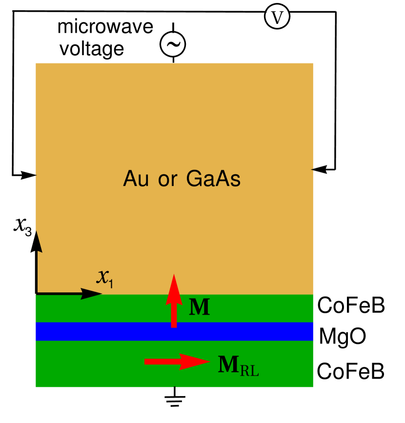
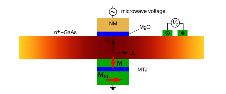
Furthermore, in MgO-based MTJs having voltage-controlled magnetic anisotropy (VCMA), magnetization oscillations can be induced in the free layer (FL) by microwave-frequency voltages even in the absence of significant STTs [21, 23, 24]. To enhance the STT acting on the FL magnetization, one can employ an MTJ with an ultrathin FL having perpendicular magnetic anisotropy [33, 34] and a thick reference layer (RL) with in-plane magnetization (Fig. 1). This feature motivated us to consider such a geometry in our study, where we focus on the Co20Fe60B20/MgO/Co20Fe60B20 junction having pronounced VCMA [22]. It should be noted that, owing to the interlayer exchange coupling (IEC) between FL and RL, the FL magnetization M slightly deviates from the perpendicular-to-plane orientation (polar angle ) even in the absence of applied voltage and external magnetic field. Therefore, the VCMA contributes to the voltage-induced destabilization of the FL magnetization along with the STT [23].
To quantify the magnetization oscillations generated by the applied ac voltage in FL with nanoscale in-plane dimensions, we use the LLGS equation and the macrospin approximation, which implies the same magnetization direction in the whole FL and a constant saturation magnetization . RL is assumed to be uniformly magnetized with a fixed magnetization direction unaffected by the applied voltage, which is confirmed by numerical calculations at the considered RL thickness nm. Since the field-like torque does not change the magnetic dynamics qualitatively [22, 35], we write the LLGS equation in the form
| (1) |
where is the electron’s gyromagnetic ratio, is the permeability of vacuum, is the Gilbert dimensionless damping parameter, and is the effective magnetic field acting on the FL magnetization. The last term in Eq. (1) allows for the STT created by the spin-polarized current flowing across FL, with the factor being proportional to the applied voltage in the first approximation. In the case of elastic tunneling in symmetric MTJs, the theoretical calculations yield , where is the elementary charge, is the reduced Planck constant, is the FL thickness, is the MTJ asymmetry factor, and and are the junction’s conductances per unit area at parallel and antiparallel electrode magnetizations, respectively [32]. To take into account the influence of the precession-induced spin pumping into a metallic or semiconducting overlayer, we renormalize the parameters and involved in Eq. (1) as [30]
| (2) |
where and denote the values of and in the absence of spin pumping, is the Landé factor, is the Bohr magneton, and is the complex reflection spin-mixing conductance per unit area of the FL-overlayer contact [36]. Since in our case the numerical estimates demonstrate a negligible dependence of the Gilbert parameter on the magnetization precession power [37], we consider as a constant quantity.
For a homogeneously magnetized ultrathin CoFeB layer, the field involved in Eq. (1) can be determined by differentiating the effective volumetric Helmholtz free-energy density of that layer. The magnetization-dependent part of this energy may be written as
| (3) |
where () are the projections of m on the crystallographic axes of the CoFeB layer, which is assumed to be epitaxial with the axis orthogonal to its surfaces, characterizes the cubic magnetocrystalline anisotropy of CoFeB [38], defines the total specific energy of the FL surfaces, is the IEC energy per unit area, are the demagnetizing factors, and the external magnetic field is absent in our case. Since the magnetic anisotropy associated with the Co20Fe60BMgO interface varies with the electric field created in MgO [34, 39], the factor appears to be a voltage-dependent quantity. In the linear approximation supported by first-principles calculations [40] and experimental data [39], , where , is the electric-field sensitivity of , and is the thickness of MgO tunnel barrier.
The numerical integration of Eq. (1) was realized with the aid of the projective Euler scheme at a fixed integration step fs. The computations were performed for the rectangular FL with nanoscale in-plane dimensions nm and nm and the thickness nm smaller than the threshold thickness nm, at which a spin reorientation transition (SRT) to the in-plane magnetization orientation takes place at . The FL demagnetizing factors were calculated analytically [41] and found to be , , and (in our case ). Other FL parameters and the conductance of the junction with a typical MgO thickness nm are listed in Table 1. Note that the magnetic anisotropy associated with the Co20Fe60Boverlayer interface [42] was neglected in comparison with that of the Co20Fe60BMgO one, and the IEC energy was evaluated via the relation mJ m-2 [43].
| Parameter | Value | Reference |
|---|---|---|
| A m-1 | [44] | |
| 0.01 | [33] | |
| 5 kJ m-3 | [45] | |
| J m-2 | [33] | |
| fJ V-1 m-1 | [39] | |
| S m-2 | [46] | |
| 0.577 | [33] | |
| 0.53 | [47] | |
| J m-2 | [43] |
The magnetization dynamics was first quantified for the Co20Fe60B20 FL covered by the Au layer with the thickness nm. The voltage drop across the Au overlayer was neglected, because its resistance is much smaller than the MTJ resistance. The displacement current proportional to the junction’s capacitance ( is the MTJ area, is the barrier permittivity [48]) was found to be insignificant in comparison with the tunnel current , because the ratio is less than 10% even at the highest studied frequency GHz. Since gold is a good heat conductor, we also ignored the FL heating caused by the microwave current, which leads to significant heat-driven spin torques in the CoFeB/MgO/FeB/MgO heterostructure [49].
To evaluate the reflection spin-mixing conductance of the Co20Fe60BAu interface, we used the theoretical estimate obtained for the FeAu one [36]. Taking m-2, from Eq. (2) we obtained for the renormalized damping parameter. Since should be negligible at the considered FL thickness nm, which is well above a few-monolayer range, the parameter was set equal to . It should be noted that the spin backflow into FL caused by the spin accumulation in the overlayer reduces the renormalized damping parameter [50]. However, this reduction increases the amplitude of magnetization oscillations and may be ignored in the first approximation at the considered thickness nm, which is much larger than the spin diffusion length nm in Au [12].
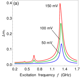
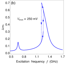
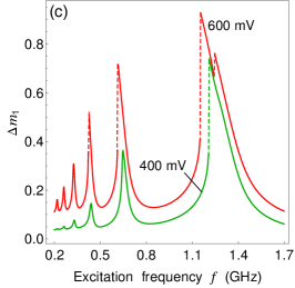
The numerical calculations were focused on the determination of the frequency dependence of magnetization precession at different amplitudes of the applied microwave voltage. As a suitable characteristic of the precession magnitude, we employed the sweep of the scalar product that governs the MTJ conductance . It was found that, at small voltages mV, the dependence involves a strong symmetric peak situated at the resonance frequency GHz and a finite number of minute peaks located at frequencies (). As the voltage increases, all peaks grow, gradually become asymmetric and shift to lower frequencies and [see Fig. 2(a)]. Remarkably, the steep segment of just below the frequency of the main peak breaks above a threshold amplitude mV [see Fig. 2(b)]. When increases up to about 600 mV, similar breaks appear at the frequencies of the secondary peaks and a second break of the main peak emerges at [Fig. 2(c)].
Peculiar dependences of the precession amplitude on the frequency of applied voltage, which appear at , are solely due to nonlinearity of the function defined by Eq. (3). Indeed, when only the STT and some fixed effective field are taken into account in the numerical calculations, the dependence assumes the standard form with a single symmetric peak situated at corresponding resonance frequency. Furthermore, the distorted shape of the main peak and the hysteresis shown in Fig. 2(b) can be explained by considering the effective field involved in Eq. (1). In the first approximation, the out-of-plane component of can be written as
| (4) |
where the sum in the brackets is negative owing to the prevailing perpendicular anisotropy created by the CoFeBMgO interface. If the excitation frequency approaches from below, the precession sweep increases, which reduces the average direction cosine of the precessing magnetization. Hence according to Eq. (4) the average effective field decreases, leading to a reduction in the resonance frequency of the large-angle precession. As a result, the precession amplitude increases further and further and eventually jumps to the right branch of the resonance curve at some frequency . On the other hand, when the excitation frequency decreases towards from above, the accompanying increase of and reduction of lower the resonance frequency. This effect extends the right branch of the resonance curve to frequencies below , but the precession amplitude drops down to the left branch at some frequency , because small decrease of does not compensate further reduction of . The above considerations explain the hysteresis of and the position of the break on the frequency scale.
The distortion of the main peak, which we revealed for the large-angle magnetization precession in the ultrathin CoFeB layer with perpendicular anisotropy, corresponds to the behavior of a Duffing oscillator with a softening nonlinearity [51]. A similar “foldover” effect was observed for the STT-driven magnetization dynamics in the Co/Ni multilayer excited by a microwave current [52]. However, such multilayer represents a hardening system due to the condition caused by the prevailing shape anisotropy. Therefore, the resonance curve should have a break on its right branch when plotted on the frequency scale, which is supported by the experimental results [52].
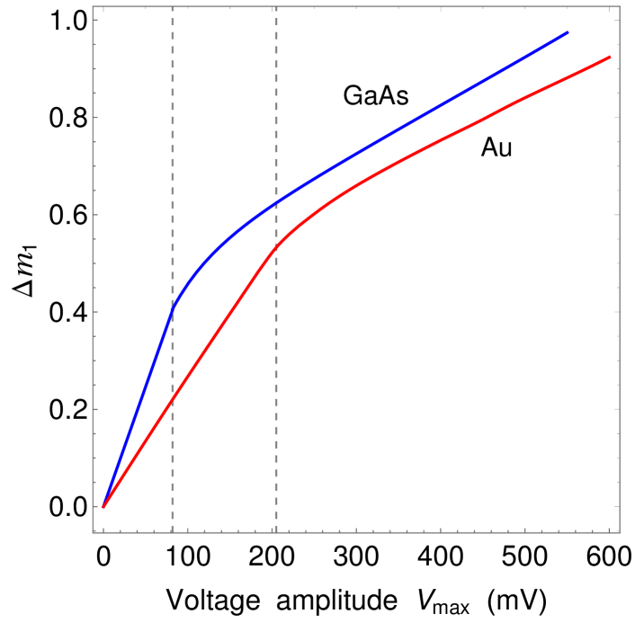
Figure 3 shows the height of the main peak appearing at increasing frequency as a function of the voltage amplitude . At , the peak height varies linearly with , but at higher voltages the variation of becomes nonlinear, which is in line with the significant change of the frequency dependence appearing above . Remarkably, continues to increase with voltage even near mV, which is due to strong STT acting on the FL magnetization at the considered small barrier thickness nm. The revealed behavior is different from the voltage dependence of the precession amplitude in the Co20Fe60B20/MgO/Co20Fe60B20 junction with the MgO thickness of 2 nm [53], which saturates at mV due to negligible STT at such . It should be noted that, in the range of small voltages , the results of our numerical calculations agree with those obtained analytically by solving the linearized LLGS equation. This agreement confirms the validity of our computations.
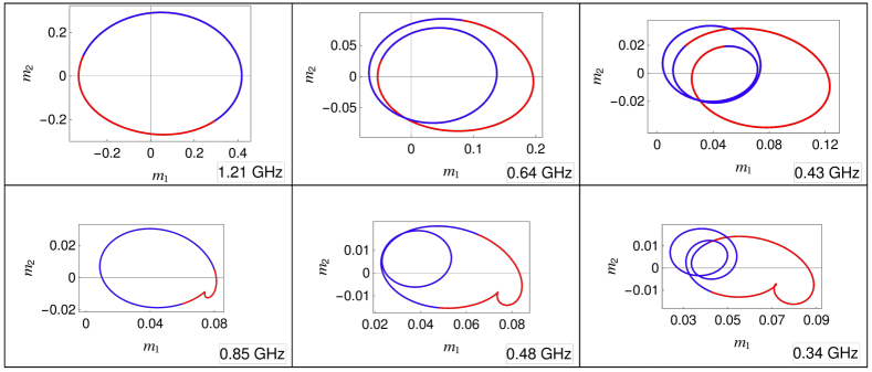
To clarify the origin of the secondary peaks, we determined the trajectories of the end of the unit vector m during the magnetization oscillations generated at different excitation frequencies for a representative voltage amplitude mV. Figure 4 shows projections of these trajectories on the plane, which arise at the frequencies and corresponding to the peaks of , in comparison with those formed at frequencies between , , and . It can be seen that, at , the magnetization makes full turns around the equilibrium direction during one period of the voltage oscillation. Since , the mean period of the forced magnetization precession appears to be close to the period of free oscillations, which explains enhancement of the precession amplitude at frequencies . Evidently, the above condition cannot be fulfilled at excitation frequencies significantly differing from . It should be noted that the predicted secondary peaks are an attribute of parametric resonance [54], which occurs when the natural oscillation frequency is varied by an external stimulus. Owing to VCMA, the application of microwave voltage modifies the absolute value of the effective field, which governs the natural precession frequency. Therefore, the presence of VCMA is responsible for the revealed secondary peaks.
Similar frequency and voltage dependences have been obtained for the electrically driven magnetization precession in the Co20Fe60B20 free layer covered by GaAs. Since the reflection spin-mixing conductance of the CoFeBGaAs interface is expected to be relatively small in comparison with that of the CoFeBAu one [15], the influence of the spin pumping on the parameters and involved in Eq. (1) can be ignored. Therefore, the magnetic damping becomes smaller (), which leads to higher peaks of in the free layer covered by GaAs. The voltage dependence of the height of the main peak appearing at increasing the excitation frequency is shown in Fig. 3. It is qualitatively similar to the voltage dependence obtained for the Co20Fe60B20 free layer covered by Au, but differs by larger values of and a smaller threshold voltage mV.
III SPIN INJECTION AND PUMPING
INTO METALLIC OVERLAYER
Using the results obtained for the magnetization dynamics induced by the microwave voltage applied to the Co20Fe60B20/MgO/Co20Fe60B20 junction, we calculated the spin current generated in the Au overlayer near the interface with FL. In our case, such current is the sum of two contributions, which result from the spin pumping caused by the magnetization precession and the spin injection proportional to the spin polarization of the charge current.
Since the spin current is characterized by the direction of spin flow and the orientation of spin polarization, we employed a second-rank tensor to define the spin-current density [55]. At the considered FL thickness, the pumped spin-current density near the Co20Fe60BAu interface can be evaluated using the formula , where is the unit normal vector to the interface pointing into Au, and may be set equal to m-2 [36]. The spin injection created by the charge current with the density is described by the relation
| (5) |
where is the spin polarization in the FL having the densities of states and of spin-up and spin-down electrons at the Fermi level, respectively. It should be noted that the spin flow along the Co20Fe60BAu interface, which is caused by the spin Hall effect, has a negligible magnitude in comparison with that of the spin flow in the direction orthogonal to the interface.
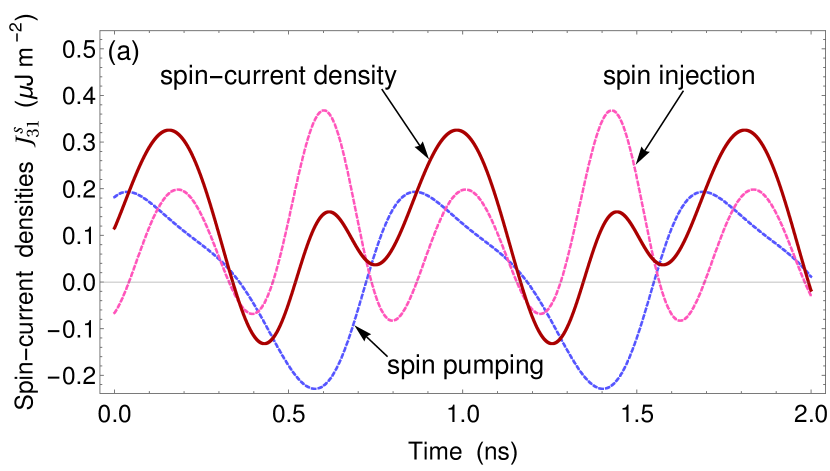
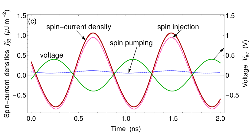
Representative results obtained for variations of the total spin-current density with time are presented in Fig. 5. Since the discussed spin current flows along the axis of our coordinate system shown in Fig. 1, the only nonzero elements of the tensor are (). Figure 5 shows that, at the considered high voltage amplitude mV, and exhibit strongly non-sinusoidal time dependences, whereas is distinguished by an approximately sinusoidal one. Concerning the contributions of precession-induced spin pumping and spin-polarized charge current, we see that the sweep of is almost the same as the one, while the sweep of is noticeably bigger than that of . In contrast, the sweep of is much larger than that of the density , which does not change sign and varies with time only slightly (Fig. 5).
The sweep characterizes the ac component of the spin-current density , and the dc component can be determined by averaging over the period of voltage oscillations. Note that and oscillate with the double excitation frequency , because the magnetization projections and involved in Eq. (5) undergo significant variations with time (see Fig. 4). Interestingly, the numerical calculations show that the spin injection does not significantly influence the ac component of the total spin-current density . Therefore, the ac component of practically equals that of , thus characterising the precession-induced spin current. Furthermore, the dc component of is almost zero so that the time-averaged value of is governed by the spin injection.
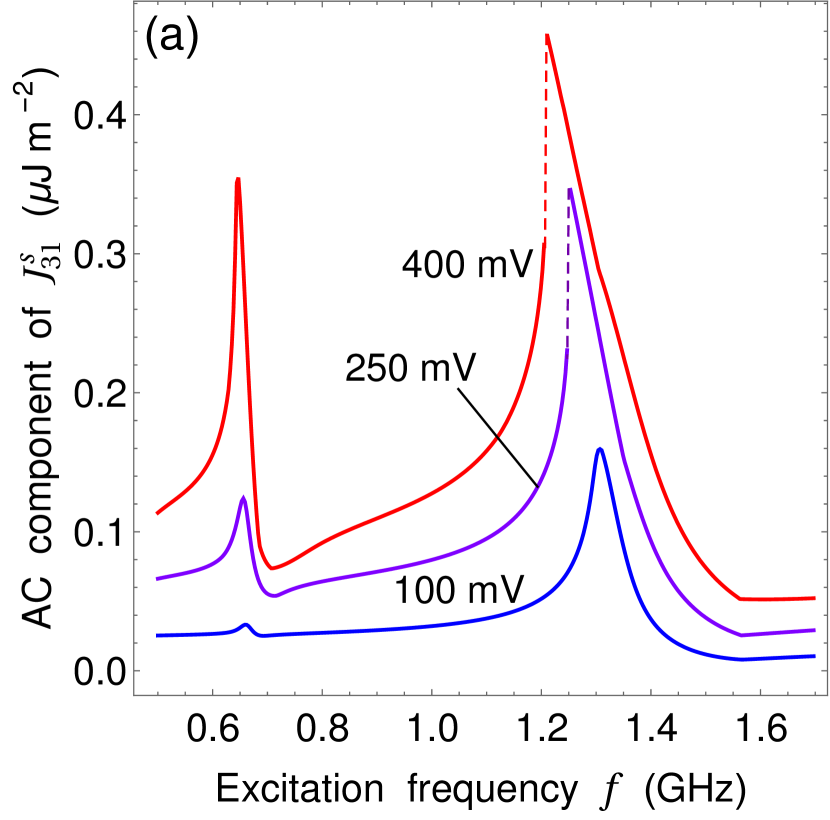
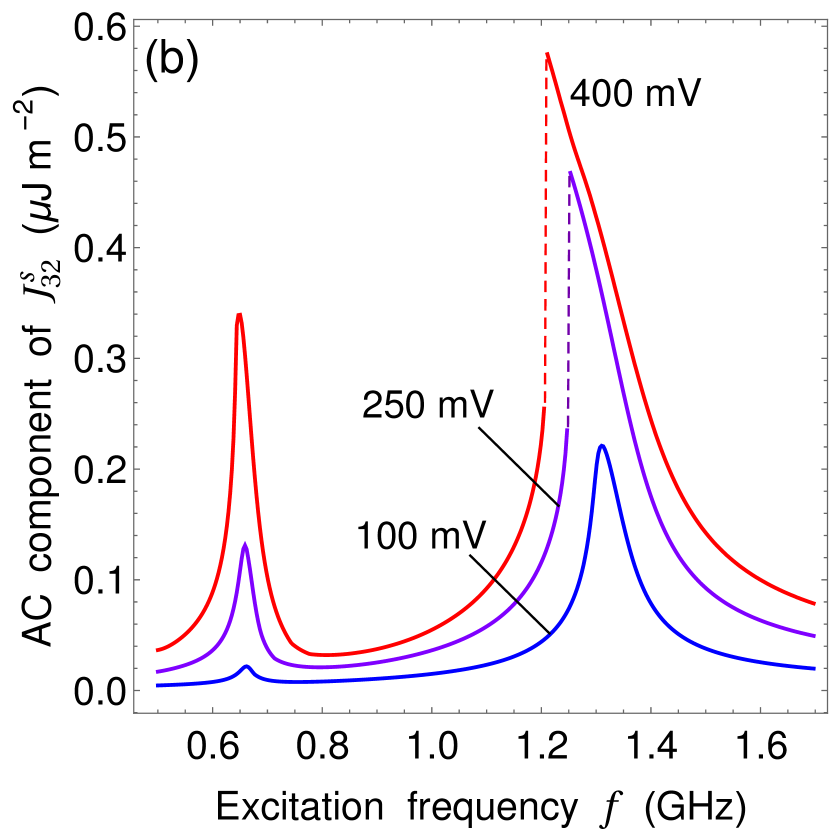
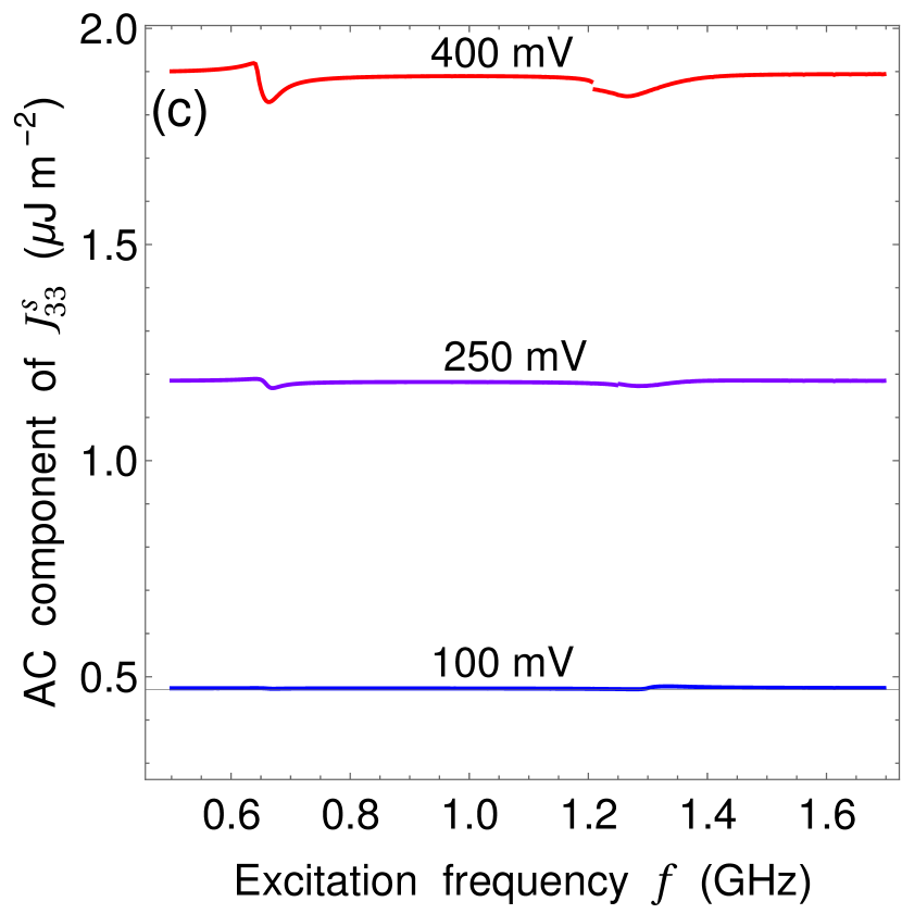
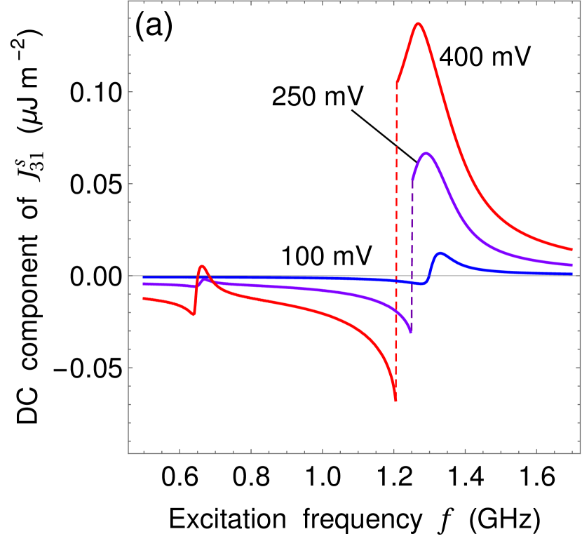
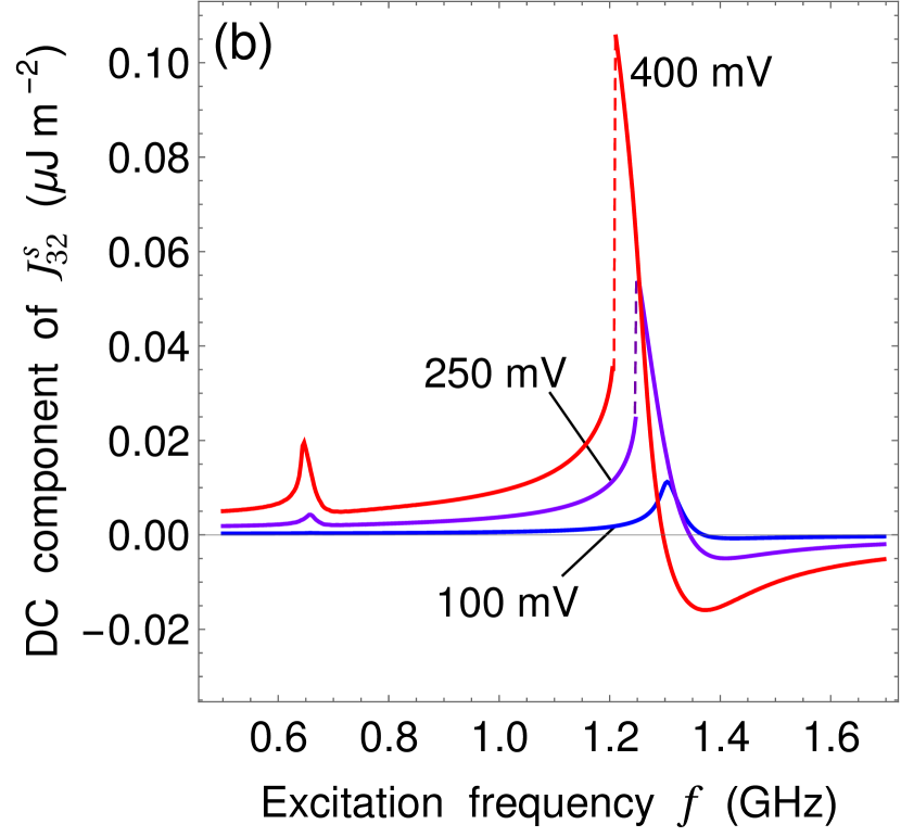
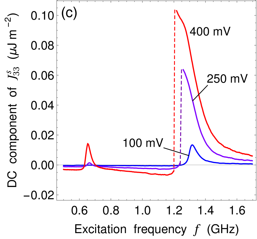
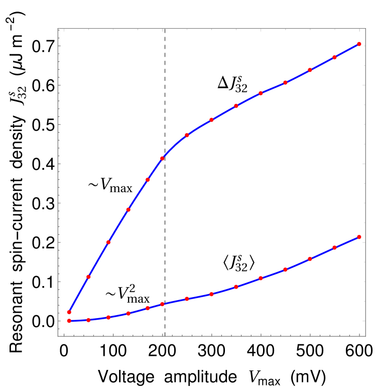
Figure 6 shows variations of the ac components , , and with the excitation frequency , which take place near the resonance frequency of the magnetization precession. It can be seen that and have a strong peak at , while only weakly depends on the excitation frequency. Remarkably, the secondary peak of and , which is located at , rapidly grows with increasing voltage amplitude and becomes comparable in magnitude with the main peak at mV. In contrast, the dc spin-current densities exhibit strong peaks near only (see Fig. 7). To illustrate the influence of the voltage amplitude on the spin-current density generated near the CoFeBAu interface, we presented in Fig. 8 the dependences and evaluated at the voltage-dependent resonance frequency . Below the threshold amplitude mV, the ac component varies with almost linearly, whereas the dc component follows the power law . At higher voltage amplitudes, both and increase slower than expected from the above dependences, but at mV they reach significantly enhanced values of about 0.7 and 0.2 J m-2, respectively. It should be noted that these values differ strongly from the spin-current densities J m-2 and J m-2 generated by the Co20Fe60B20/MgO/Co20Fe60B20 MTJ excited by direct charge current [56].
The spin-current densities presented in Figs. 5-8 are partially suppressed at the interface by the spin backflow The product consists of the components parallel and perpendicular to the magnetization direction m, which are caused by spin injection and spin pumping, respectively [see Eq. (5) and expression for spin pumping]. Numerical estimates show that the conductance mismatch problem does not appear for the CoFeBAu interface. Accordingly, the longitudinal spin backflow is negligible compared to in our case. In contrast, the transverse spin backflow reduces the spin pumping significantly. To calculate the actual spin-current density in Au, we solve the spin diffusion equation with appropriate boundary conditions for spin injection and pumping. The boundary condition at represents zero spin flux. The boundary condition at the interface reads [8], where is the spin accumulation in Au near the interface. It should be noted that in our case , where and are the densities of states in Au, which characterize spin-up and spin-down electrons at the Fermi level. The introduction of spin accumulation allows to express the diffusive spin-current density in Au as [57], where is the electrical conductivity of Au. Solving the diffusion equation in the adiabatic approximation [57], we obtain an analytic relation
| (6) |
which describes how decays with the distance from the CoFeBAu interface due to spin relaxation and diffusion. Equation (6) is similar to the formula presented in [12], but differs by the spin-current density at the interface , where is the backflow factor. Taking S m-1 [58], we find so that the actual spin pumping into Au is smaller than by about 40%.
Our theoretical results demonstrate that the CoFeB/MgO/CoFeB tunnel junction subjected to a microwave voltage with an appropriate frequency represents a promising spin injector into normal metals. Since the generated spin current creates a charge current owing to the inverse spin Hall effect (ISHE), the efficiency of spin injection can be probed electrically [11]. Motivated by this opportunity, we calculated distributions of the charge-current density and electric potential in the Au overlayer in the quasistatic approximation [56]. As the ISHE contribution to the density is governed by the vector product of the spin accumulation and the unit vector directed along the spin flow [59], the element of the spin-current-density tensor does not affect and can be disregarded. Further, the elements and create contributions only to the projections of on the orthogonal axes and , respectively. Restricting our calculations to the determination of the charge transport in the plane, which governs the transverse voltage between the sides of Au overlayer normal to the axis (Fig. 1), we may disregard as well. For the relevant projection of the ISHE current density, the theory gives , where is the spin Hall angle of Au [12], and the spin-current density is determined by Eq. (6).
The total density of the charge current flowing in the Au layer is the sum of the ISHE contribution and the drift contribution . To calculate the electric potential , we used the Laplace’s equation appended by appropriate boundary conditions. Namely, the charge-current density at the CoFeBAu interface was set equal to the density of the tunnel current, which was assumed uniform, because the anomalous Hall effect in the CoFeB layer has a weak effect on the transverse voltage [56].
The same boundary condition was introduced at the upper boundary of the Au overlayer to exclude the charge accumulation in Au. At the side boundaries and of the overlayer, the total current density should go to zero, which yields , where is directly proportional to the spin-current density given by Eq. (6). Remarkably, because of this condition the transverse voltage at any time moment is a linear combination of and presented in Fig. 5. Taking into account that and , we find that the ac component of the transverse voltage is proportional to spin pumping, whereas the dc component is proportional to spin injection. Hence a certain tunneling heterostructure has the universal dependences of the normalized voltages and on the distance from the interface, which do not depend on the amplitude and frequency of the electrical excitation.
For the considered spin injector, the numerical calculations demonstrate that the variations of and follow the curves shown in Fig. 9. Thus, using the curves in Fig. 9 together with the data presented in Fig. 8, one can evaluate the voltage swing induced by the spin pumping and the time-averaged transverse voltage proportional to the spin injection. At mV and GHz, the calculation yields nV and nV for the Au region nm near the interface. The predicted transverse voltages can be detected experimentally, which indicates significant efficiency of the proposed spin injector.
IV SPIN PUMPING INTO SEMICONDUCTOR
To demonstrate that MTJs excited by microwave voltages can be employed as efficient spin injectors into semiconductors too, we study the spin accumulation in a long GaAs bar connected to the CoFeB/MgO/CoFeB junction and separated from a normal-metal (NM) lead by a thin MgO interlayer (see Fig. 10). The length of the GaAs bar is much larger than the FL size along the axis, while its width along the axis is equal to the FL size . The considered Si-doped GaAs with the donor concentration cm-3 is a degenerate semiconductor [60], which forms an Ohmic contact with CoFeB. Indeed, n+-GaAs has the electron mobility m2 V-1 s-1 [61] and the conductivity S m-1, which is only one order of magnitude smaller than the conductivity S m-1 of CoFeB [62]. From the measured spin-flip relaxation time ns [63] and the diffusion coefficient m2 s-1 obtained via the Einstein relation it follows that the spin-diffusion length in n+-GaAs amounts to about 2.32 m at room temperature. Hence the spin accumulation , which is the difference between the chemical potentials for spins parallel and antiparallel to the direction determined by the total nonequilibrium spin-imbalance density [8], should be homogeneous in the considered GaAs bar with the nanoscale thickness nm along the axis normal to the CoFeBGaAs interface. Assuming to be uniform along the axis as well, we obtain a one-dimensional diffusion equation ( is the Boltzmann constant)
| (7) |
for the sought function . The first term on the r. h. s. of Eq. (7) differs from zero only at and describes the spin generation in the bar section adjacent to FL. The total spin-current density is the sum of four contributions, which result from the spin pumping into GaAs (), spin injection from FL into GaAs (), spin backflow from GaAs to FL (), and spin loss caused by the spin-polarized tunnel current flowing across the MgO interlayer separating GaAs from the NM lead (). The spin-injection density can be calculated using Eq. (5), where the FL spin polarization should be replaced by the effective polarization [5] depending on the CoFeB spin-diffusion length nm [64]. With the numerical values of the involved parameters the calculation gives very small effective polarization , which means that the spin injection into n+-GaAs is negligible due to small product in comparison with . Accordingly, the spin-accumulation vector appears to be almost orthogonal to the FL magnetization M, and the spin backflow from GaAs to FL can be evaluated via the relation [30]. Finally, the spin loss caused by the charge current flowing across the GaAsMgO interface equals . The distribution of spin accumulation along the GaAs bar was calculated by solving Eq. (7) numerically with the boundary condition at . We assumed that the MgO tunnel barrier separating GaAs from the NM lead has the same conductance as the CoFeB/MgO/CoFeB junction in the state with parallel electrode magnetizations. Since the GaAs resistance is negligible in comparison with that of two MgO barriers, the dependence of the charge current on voltage applied to the whole heterostructure was approximated by the relation . The electrically induced dynamics of the FL magnetization was recalculated with the account of the modified and VCMA resulting from a lower voltage applied to the MTJ. The spin-pumping contribution to the total spin-current density involved in Eq. (7) was evaluated using the spin-mixing conductance m-2 determined experimentally for the Ni81FeGaAs interface [15].
The numerical calculations showed that the spin accumulation in GaAs is determined by the competition of spin pumping and spin backflow across the CoFeBGaAs interface, while the spin loss through the GaAsMgO interface is negligible in comparison with . Further, the differences between nonzero components of and are about 1% only, which shows that near the CoFeBGaAs interface the spin accumulation is close to saturation. Taking into account that only and create significant contributions to , we solved Eq. (7) analytically. Since the spin-flip relaxation time ns is comparable to the period ns of magnetization precession, the quasistatic approximation cannot be employed, and should be regarded as a complex quantity. After some mathematical operations, we obtained the following relation between the Fourier components of and :
| (8) |
where and . By combining Eq. (8) with numerical results obtained for the electrically driven precession of the FL magnetization and the accompanying spin pumping , one can calculate the spin accumulation as a function of the distance from the bar center and the time . At small frequencies , the parameter is real, and the phase of does not depend on the position . However, at the precession frequencies GHz the spin accumulation has a position-dependent delay from the applied voltage .
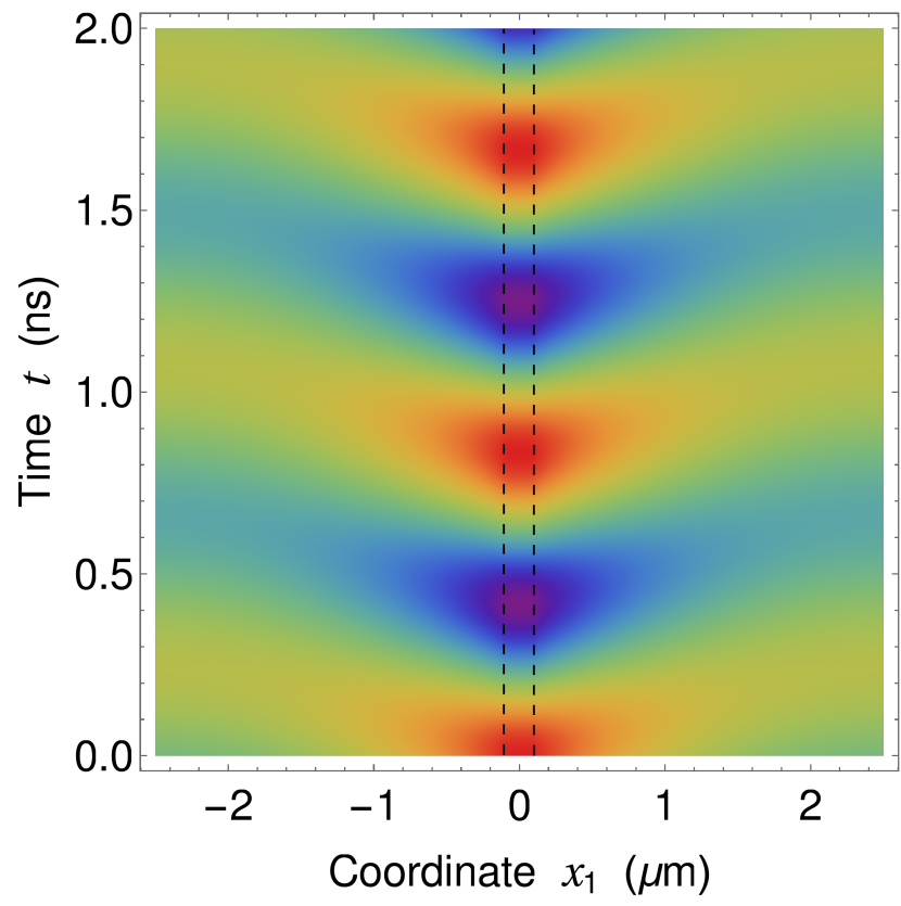
Figure 11 shows the spatio-temporal map of the spin-accumulation component generated in 5-m-long n+-GaAs bar by the applied voltage with amplitude mV and frequency GHz. Since this frequency corresponds to the main peak of the magnetization precession, we assume that and exhibit almost simple harmonic oscillations with the excitation frequency . However, these oscillations lag behind the applied microwave voltage by about 0.25 ns at in the 5-m-long bar (see Fig. 11).
The averaging of over the oscillation period shows that the mean spin accumulation is negligible in comparison with the oscillation amplitude . The maps presented in Fig. 12 demonstrate how the magnitude of applied microwave voltage influences the spatial distribution of calculated at the voltage-dependent resonance frequency . Remarkably, the ac component of the spin accumulation remains significant even at the ends of the considered GaAs bars with the length ranging from 2 to 5 m. When is smaller than the spin diffusion length m, appears to be weakly dependent on the coordinate near the bar ends [Fig. 12(a)]. In contrast, it decreases more rapidly with the distance from the bar center at [Fig. 12(b)] and becomes smaller everywhere due to the spreading of nonequilibrium spin imbalance in a larger volume.
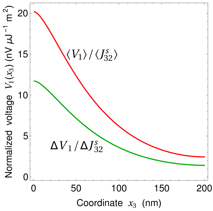
The spin accumulation in the GaAs bar can be measured experimentally by a method similar to a nonlocal detection of the spin injection into a normal conductor [3, 65]. The method employs two ferromagnetic nanostrips integrated onto the bar surface and connected to a voltmeter (see Fig. 10). The nanostrips should be oriented along the axis and have antiparallel in-plane magnetizations. The presence of the spin accumulation in the GaAs region beneath ferromagnetic strips with nanoscale widths nm and small separation manifests itself in a voltage between the nanocontacts. In the case of Fe nanocontacts forming Schottky tunnel barriers with n+-GaAs, , where is the spin transmission efficiency of the GaAsFe interface and is the spin polarization of Fe at the Fermi level [65]. Using this relation, we calculated frequency spectra of the spin signals generated in the 0.8-m-long n+-GaAs bar at different excitation frequencies .
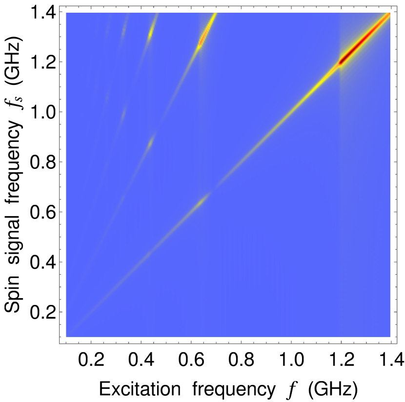
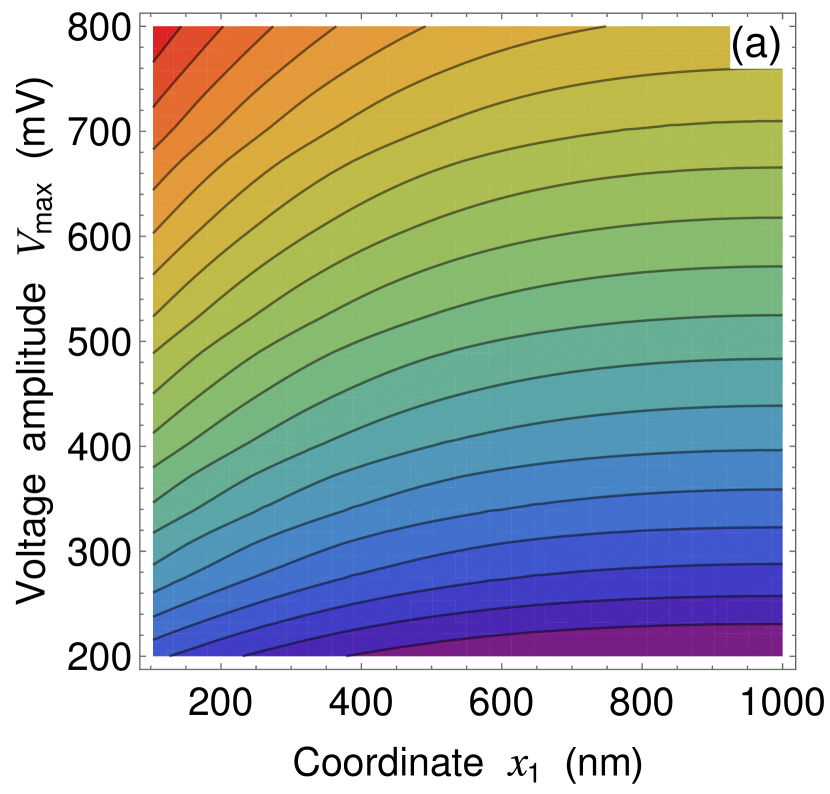
The map presented in Fig. 13 demonstrates amplitudes of the Fourier components of determined at mV and the distance nm from the bar center. It can be seen that the maximal ac spin signal with the amplitude of about 0.26 V and frequency appears at the excitation frequencies GHz close to the resonance frequency .
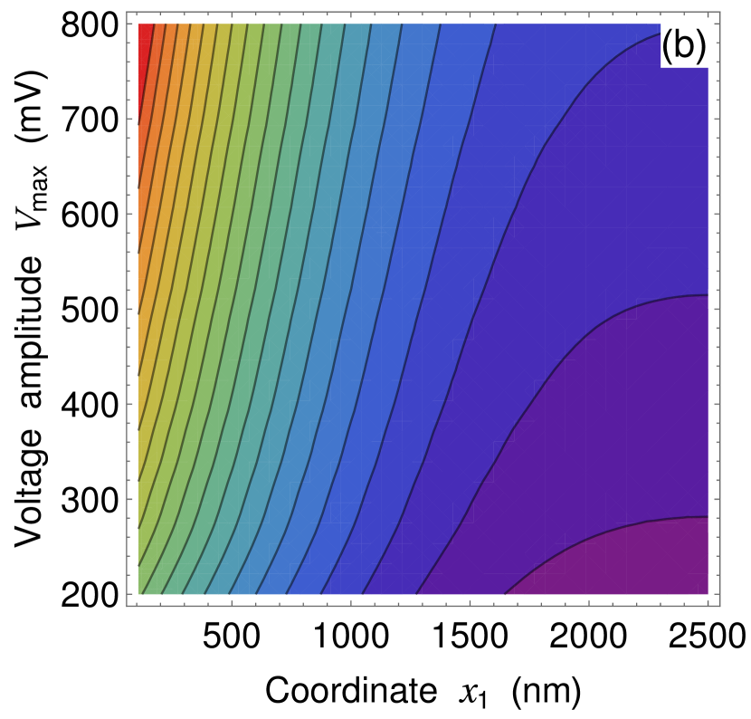
In addition, the Fourier components of with frequencies slightly above exhibit smaller maxima at the excitation frequencies , which correspond to secondary peaks of the precession amplitude similar to those shown in Fig. 2(c). Remarkably, such spin signals have significant amplitudes ranging from 0.12 V at to 0.04 V at , which can be detected experimentally. Thus, the proposed spin injector allows the generation of the ac spin accumulation in GaAs oscillating with the microwave frequency several times higher than the excitation frequency. Such frequency multiplication could be useful for device applications.
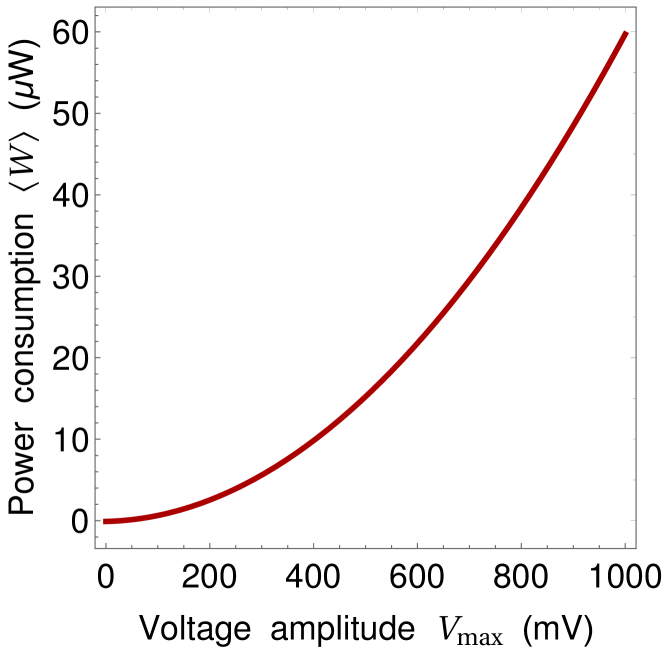
The mean power consumption of the proposed spin injector can be estimated from the relation
| (9) |
where the integral is taken over the period of an applied ac voltage. Figure 14 shows the dependence calculated for the CoFeB/MgO/CoFeB/GaAs/MgO heterostructure considered in this work. It can be seen that rises rapidly with the voltage amplitude, but remains well below 100 W even at V. Hence the power dissipation of the electrically driven spin injector is more than two orders of magnitude smaller than that of the device excited by the microwave magnetic field ( mW) [15].
V CONCLUSIONS
In this paper, we theoretically described the spin dynamics in the Co20Fe60B20/MgO/Co20Fe60B20/Au and Co20Fe60B20/MgO/Co20Fe60B20/GaAs heterostructures subjected to a microwave voltage. Our calculations were focused on the heterostructures comprising a nanoscale Co20Fe60B20/MgO/Co20Fe60B20 tunnel junction with an ultrathin FL having perpendicular magnetic anisotropy (Fig. 1). By solving the LLGS equation numerically, we first quantified the electrically induced precession of FL magnetization with the account of STT created by the spin-polarized current flowing through FL, VCMA associated with the FLMgO interface, and enhanced Gilbert damping caused by the spin pumping into the overlayer. The calculated dependences of the precession amplitude on the frequency and magnitude of the applied voltage showed that FL exhibits strongly nonlinear dynamic behavior at mV. In particular, the main peak of precession amplitude located at the resonance frequency becomes asymmetric with a break on the left side [Fig. 2(b)], which is similar to the behavior of a Duffing oscillator with a softening nonlinearity [51]. At higher applied voltages mV, the frequency dependence of precession amplitude also involves strong secondary peaks and additional breaks [Fig. 2(c)].
The description of the magnetization dynamics occuring in the Co20Fe60B20 FL enabled us to quantify the spin injection and pumping into the Au and GaAs overlayers. The total spin-current densities generated near the interface were calculated as a function of time at different frequencies and amplitudes of the applied voltage (Fig. 5). The analysis of these time dependences showed that the densities contain both ac and dc components, which mostly maximize under resonant excitation (Figs. 6 and 7). Interestingly, the ac components and also strongly increase at the excitation frequencies and high voltage amplitudes mV.
To evaluate the efficiency of spin generation in Au, we determined the distribution of electric potential in the 200-nm-thick Au overlayer by solving the Laplace’s equation. The charge current flowing in the overlayer was calculated with the account of the drift contribution and the inverse spin Hall effect. When finding the spatial distribution of the actual spin-current density we considered the spin injection and pumping at the FLAu interface, spin relaxation and diffusion inside Au, and the spin backflow into FL. The calculated distribution of the electric potential was used to determine the transverse voltage between the sides of Au overlayer normal to the axis parallel to the RL magnetization. It was found that both ac and dc components of this time-dependent voltage can be measured experimentally at small distances nm from the FLAu interface under excitation by the microwave voltage with and mV. The measured dependence provides information on the spatial decay of the actual spin-current density reduced by spin backflow into FL and spin relaxation in Au.
In the final part of this study, we quantified the time-dependent spin accumulation in the n+-GaAs bar coupled to the CoFeB/MgO/CoFeB junction at the center and separated from the NM lead by a thin MgO interlayer (Fig. 10). By solving numerically the spin diffusion equation with appropriate boundary conditions, we calculated the spatio-temporal map of the spin-accumulation component in the bar (Fig. 11). It was revealed that there is a position-dependent delay of from the applied microwave voltage . The time-averaged value of the oscillating spin accumulation was found to be negligible in comparison with the oscillation amplitude . At the same time, the ac component of the spin accumulation under resonant excitation remained to be significant even at the ends of the 5-m-long n+-GaAs bar. To detect this component, we proposed to use two ferromagnetic nanostrips integrated onto the bar surface and connected to a voltmeter (Fig. 10). The voltage between such nanocontacts and its frequency spectrum were calculated. The results showed that the maximal ac spin signal appears at the excitation frequencies GHz close to the resonance frequency . Its frequency is equal to the excitation one, and the amplitude is about 0.26 V at a representative distance nm from the bar center. In addition, the Fourier components of with frequencies slightly above exhibit significant maxima at the excitation frequencies about and . These results demonstrate high efficiency of the described nanoscale spin injector and the possibility of ac spin accumulation with frequency multiplication. It should be noted that the proposed device is distinguished from the spin injector driven by a microwave magnetic field [15] by a compact design and low power consumption.
Acknowledgements.
This work was supported by the Foundation for the Advancement of Theoretical Physics and Mathematics “BASIS”.References
- Žutić and Sarma [2004] J. F. Žutić and S. D. Sarma, Spintronics: Fundamentals and applications, Rev. Mod. Phys. 76, 323 (2004).
- Dery et al. [2007] H. Dery, P. Dalal, L. Cywinski, and L. J. Sham, Spin-based logic in semiconductors for reconfigurable large-scale circuits, Nature 447, 573 (2007).
- Johnson and Silsbee [1985] M. Johnson and R. H. Silsbee, Interfacial charge-spin coupling: injection and detection of spin magnetization in metals, Phys. Rev. Lett. 55, 1790 (1985).
- Jedema et al. [2001] F. J. Jedema, A. T. Filip, and B. J. van Wees, Electrical spin injection and accumulation at room temperature in an all-metal mesoscopic spin valve, Nature 410, 345 (2001).
- Schmidt et al. [2000] G. Schmidt, D. Ferrand, L. W. Molenkamp, A. T. Filip, and B. J. van Wees, Fundamental obstacle for electrical spin injection from a ferromagnetic metal into a diffusive semiconductor, Phys. Rev. B 62, R4790 (2000).
- Rashba [2000] E. I. Rashba, Theory of electrical spin injection: Tunnel contacts as a solution of the conductivity mismatch problem, Phys. Rev. B 62, R16267 (2000).
- Jiang et al. [2005] X. Jiang, R. Wang, R. M. Shelby, R. M. Macfarlane, S. R. Bank, J. S. Harris, and S. S. Parkin, Highly spin-polarized room-temperature tunnel injector for semiconductor spintronics using MgO(100), Phys. Rev. Lett. 94 (2005).
- Tserkovnyak et al. [2005] Y. Tserkovnyak, A. Brataas, G. E. W. Bauer, and B. I. Halperin, Nonlocal magnetization dynamics in ferromagnetic heterostructures, Rev. Mod. Phys. 77, 1375 (2005).
- Brataas et al. [2002] A. Brataas, Y. Tserkovnyak, G. E. W. Bauer, and B. I. Halperin, Spin battery operated by ferromagnetic resonance, Phys. Rev. B 66 (2002).
- Heinrich et al. [2003] B. Heinrich, Y. Tserkovnyak, G. Woltersdorf, A. Brataas, R. Urban, and G. E. W. Bauer, Dynamic Exchange Coupling in Magnetic Bilayers, Phys. Rev. Lett. 90 (2003).
- Saitoh et al. [2006] E. Saitoh, M. Ueda, H. Miyajima, and G. Tatara, Conversion of spin current into charge current at room temperature: Inverse spin-Hall effect, Appl. Phys. Lett. 88 (2006).
- Mosendz et al. [2010a] O. Mosendz, V. Vlaminck, J. E. Pearson, F. Y. Fradin, G. E. W. Bauer, S. D. Bader, and A. Hoffmann, Detection and quantification of inverse spin Hall effect from spin pumping in permalloy/normal metal bilayers, Phys. Rev. B 82 (2010a).
- Sandweg et al. [2010] C. W. Sandweg, Y. Kajiwara, K. Andoa, E. Saitoh, and B. Hillebrands, Enhancement of the spin pumping efficiency by spin wave mode selection, Appl. Phys. Lett. 97 (2010).
- Ando et al. [2011a] K. Ando, S. Takahashi, J. Ieda, Y. Kajiwara, H. Nakayama, T. Yoshino, K. Harii, Y. Fujikawa, M. Matsuo, S. Maekawa, and E. Saitoh, Inverse spin-Hall effect induced by spin pumping in metallic system, J. Appl. Phys. 109 (2011a).
- Ando et al. [2011b] K. Ando, S. Takahashi, J. Ieda, H. Kurebayashi, T. Trypiniotis, C. H. W. Barnes, S. Maekawa, and E. Saitoh, Electrically tunable spin injector free from the impedance mismatch problem, Nat. Mat. 10, 655 (2011b).
- Shikoh et al. [2013] E. Shikoh, K. Ando, K. Kubo, E. Saitoh, T. Shinjo, and M. Shiraishi, Spin-Pump-Induced Spin Transport in p-Type Si at Room Temperature, Phys. Rev. Lett. 110 (2013).
- Kiselev et al. [2003] S. I. Kiselev, J. C. Sankey, I. N. Krivorotov, N. C. Emley, R. J. Schoelkopf, R. A. Buhrman, and D. C. Ralph, Microwave oscillations of a nanomagnet driven by a spin-polarized current, Nature (London) 425, 380 (2003).
- Tulapurkar et al. [2005] A. A. Tulapurkar, Y. Suzuki, A. Fukushima, H. Kubota, H. Maehara, K. Tsunekawa, D. D. Djayaprawira, N. Watanabe, and S. Yuasa, Spin-torque diode effect in magnetic tunnel junctions, Nature (London) 438, 339 (2005).
- Sankey et al. [2006] J. C. Sankey, P. M. Braganca, A. G. F. Garcia, I. N. Krivorotov, R. A. Buhrman, and D. C. Ralph, Spin-Transfer-Driven Ferromagnetic Resonance of Individual Nanomagnets, Phys. Rev. Lett. 96 (2006).
- Deac et al. [2008] M. Deac, A. Fukushima, H. Kubota, H. Maehara, Y. Suzuki, S. Yuasa, Y. Nagamine, K. Tsunekawa, D. D. Djayaprawira, and N. Watanabe, Bias-driven high-power microwave emission from MgO-based tunnel magnetoresistance devices, Nat. Phys. 4, 803 (2008).
- Nozaki et al. [2012] T. Nozaki, Y. Shiota, S. Miwa, S. Murakami, F. Bonell, S. Ishibashi, H. Kubota, K. Yakushiji, T. Saruya, A. Fukushima, S. Yuasa, T. Shinjo, and Y. Suzuki, Electric-field-induced ferromagnetic resonance excitation in an ultrathin ferromagnetic metal layer, Nat. Phys. 8, 491 (2012).
- Zhu et al. [2012] J. Zhu, J. A. Katine, G. E. Rowlands, Y.-J. Chen, Z. Duan, J. G. Alzate, P. Upadhyaya, J. Langer, P. K. Amiri, K. L. Wang, and I. N. Krivorotov, Voltage-Induced Ferromagnetic Resonance in Magnetic Tunnel Junctions, Phys. Rev. Lett. 108 (2012).
- Viaud and Pertsev [2014] G. Viaud and N. A. Pertsev, Dynamic converse magnetoelectric effect in ferromagnetic nanostructures with electric-field-dependent interfacial anisotropy, Phys. Rev. B 90 (2014).
- Miura et al. [2017] K. Miura, S. Yabuuchi, M. Yamada, M. Ichimura, B. Rana, S. Ogawa, H. Takahashi, Y. Fukuma, and Y. Otani, Voltage-induced magnetization dynamics in CoFeB/MgO/CoFeB magnetic tunnel junctions, Sci. Rep. 7 (2017).
- Weiler et al. [2011] M. Weiler, L. Dreher, C. Heeg, H. Huebl, R. Gross, M. S. Brandt, and S. T. B. Goennenwein, Elastically Driven Ferromagnetic Resonance in Nickel Thin Films, Phys. Rev. Lett. 106 (2011).
- Weiler et al. [2012] M. Weiler, H. Huebl, F. S. Goerg, F. D. Czeschka, R. Gross, and S. T. B. Goennenwein, Spin Pumping with Coherent Elastic Waves, Phys. Rev. Lett. 108 (2012).
- Azovtsev and Pertsev [2016] A. V. Azovtsev and N. A. Pertsev, Magnetization dynamics and spin pumping induced by standing elastic waves, Phys. Rev. B 94 (2016).
- Polzikova et al. [2018] N. I. Polzikova, S. G. Alekseev, V. A. Luzanov, and A. O. Raevskiy, Electroacoustic Excitation of Spin Waves and Their Detection due to the Inverse Spin Hall Effect, Phys. Solid State 60, 2211 (2018).
- Azovtsev and Pertsev [2019] A. V. Azovtsev and N. A. Pertsev, Dynamical spin phenomena generated by longitudinal elastic waves traversing CoFe2O4 films and heterostructures, Phys. Rev. B 100 (2019).
- Tserkovnyak et al. [2002] Y. Tserkovnyak, A. Brataas, and G. E. W. Bauer, Enhanced Gilbert Damping in Thin Ferromagnetic Films, Phys. Rev. Lett. 88 (2002).
- Slonczewski [1989] J. C. Slonczewski, Conductance and exchange coupling of two ferromagnets separated by a tunneling barrier, Phys. Rev. B 39 (1989).
- Slonczewski and Sun [2007] J. C. Slonczewski and J. Z. Sun, Theory of voltage-driven current and torque in magnetic tunnel junctions, J. Magn. Magn. Mater. 310, 169 (2007).
- Ikeda et al. [2010] S. Ikeda, K. Miura, H. Yamamoto, K. Mizunuma, H. D. Gan, M. Endo, S. Kanai, J. Hayakawa, F. Matsukura, and H. Ohno, A perpendicular-anisotropy CoFeB–MgO magnetic tunnel junction, Nat. Mater. 9, 721 (2010).
- Kanai et al. [2012] S. Kanai, M. Yamanouchi, S. Ikeda, Y. Nakatani, F. Matsukura, and H. Ohno, Electric field-induced magnetization reversal in a perpendicular-anisotropy CoFeB-MgO magnetic tunnel junction, Appl. Phys. Lett. 101 (2012).
- Fang et al. [2016] B. Fang, M. Carpentieri, X. Hao, H. Jiang, J. A. Katine, I. N. Krivorotov, B. Ocker, J. Langer, K. L. Wang, B. Zhang, B. Azzerboni, P. K. Amiri, G. Finocchio, and Z. Zeng, Giant spin-torque diode sensitivity in the absence of bias magnetic field, Nat. Commun. 7 (2016).
- Zwierzycki et al. [2005] M. Zwierzycki, Y. Tserkovnyak, P. J. Kelly, A. Brataas, and G. E. W. Bauer, First-principles study of magnetization relaxation enhancement and spin transfer in thin magnetic films, Phys. Rev. B 71 (2005).
- Slavin and Tiberkevich [2009] A. Slavin and V. Tiberkevich, Nonlinear Auto-Oscillator Theory of Microwave Generation by Spin-Polarized Current, IEEE Transactions on Magnetics 45, 1875 (2009).
- Ikeda et al. [2012] S. Ikeda, R. Koizumi, H. Sato, M. Yamanouchi, K. Miura, K. Mizunuma, H. Gan, F. Matsukura, and H. Ohno, Boron Composition Dependence of Magnetic Anisotropy and Tunnel Magnetoresistance in MgO/CoFe(B) Based Stack Structures, IEEE Transactions on Magnetics 48, 3829 (2012).
- Alzate et al. [2014] J. G. Alzate, P. K. Amiri, G. Yu, P. Upadhyaya, J. A. Katine, J. Langer, B. Ocker, I. N. Krivorotov, and K. L. Wang, Temperature dependence of the voltage-controlled perpendicular anisotropy in nanoscale MgOCoFeBTa magnetic tunnel junctions, Appl. Phys. Lett. 104 (2014).
- Niranjan et al. [2010] M. K. Niranjan, C.-G. Duan, S. S. Jaswal, and E. Y. Tsymbal, Electric field effect on magnetization at the Fe/MgO(001) interface, Appl. Phys. Lett. 96 (2010).
- Aharoni [1998] A. Aharoni, Demagnetizing factors for rectangular ferromagnetic prisms, J. Appl. Phys. 83, 3432 (1998).
- Peng et al. [2017] S. Peng, W. Zhao, J. Qiao, L. Su, J. Zhou, H. Yang, Q. Zhang, Y. Zhang, C. Grezes, P. K. Amiri, and K. L. Wang, Giant interfacial perpendicular magnetic anisotropy in MgO/CoFe/capping layer structures, Appl. Phys. Lett. 110 (2017).
- Skowroński et al. [2010] W. Skowroński, T. Stobiecki, J. Wrona, K. Rott, A. Thomas, G. Reiss, and S. van Dijken, Interlayer exchange coupling and current induced magnetization switching in magnetic tunnel junctions with MgO wedge barrier, J. Appl. Phys. 107 (2010).
- Lee et al. [2011] K. Lee, J. J. Sapan, S. H. Kang, and E. E. Fullerton, Perpendicular magnetization of CoFeB on single-crystal MgO, Appl. Phys. Lett. 109 (2011).
- Hall [1960] R. C. Hall, Magnetic Anisotropy and Magnetostriction of Ordered and Disordered Cobalt-Iron Alloys, J. Appl. Phys. 31 (1960).
- Tsunekawa et al. [2005] K. Tsunekawa, M. Nagai, H. Maehara, S. Yamagata, D. D. Djayaprawira, N. Watanabe, S. Yuasa, Y. Suzuki, and K. Ando, CoFeB/MgO/CoFeB magnetic tunnel junctions with high TMR ratio and low junction resistance, in 2005 IEEE International Magnetics Conference (INTERMAG) (2005) pp. 1223–1224.
- Huang et al. [2008] S. X. Huang, T. Y. Chen, and C. L. Chien, Spin polarization of amorphous CoFeB determined by point-contact Andreev reflection, Appl. Phys. Lett. 92, 242509 (2008).
- Fontanella et al. [1974] J. Fontanella, C. Andeen, and D. Schuele, Low‐frequency dielectric constants of ‐quartz, sapphire, MgF2, and MgO, J. Appl. Phys. 45, 2852 (1974).
- Goto et al. [2019] M. Goto, Y. Wakatake, U. K. Oji, S. Miwa, N. Strelkov, B. Dieny, H. Kubota, K. Yakushiji, A. Fukushima, S. Yuasa, and Y. Suzuki, Microwave amplification in a magnetic tunnel junction induced by heat-to-spin conversion at the nanoscale, Nat. Nanotech. 4, 40 (2019).
- Jiao and Bauer [2013] H. Jiao and G. E. W. Bauer, Spin Backflow and ac Voltage Generation by Spin Pumping and the Inverse Spin Hall Effect, Phys. Rev. Lett. 110 (2013).
- Nayfeh and Mook [1979] A. H. Nayfeh and D. T. Mook, Nonlinear Oscillations (Wiley, New York, 1979).
- Chen et al. [2009] W. Chen, G. de Loubens, J.-M. L. Beaujour, J. Z. Sun, and A. D. Kent, Spin-torque driven ferromagnetic resonance in a nonlinear regime, Appl. Phys. Lett. 95 (2009).
- Rana et al. [2017] B. Rana, Y. Fukuma, K. Miura, H. Takahashi, and Y. Otani, Effect of excitation power on voltage induced local magnetization dynamics in an ultrathin CoFeB film, Sci. Rep. 7 (2017).
- Jia et al. [2016] Y. Jia, S. Du, and A. A. Seshia, Twenty-Eight Orders of Parametric Resonance in a Microelectromechanical Device for Multi-band Vibration Energy Harvesting, Sci. Rep. 6 (2016).
- Dyakonov and Perel [1971] M. I. Dyakonov and V. I. Perel, Current-induced spin orientation of electrons in semiconductors, Phys. Lett. A 35, 459 (1971).
- Nikitchenko and Pertsev [2019] A. I. Nikitchenko and N. A. Pertsev, Spin injection and pumping generated by a direct current flowing through a magnetic tunnel junction, Phys. Rev. B 99 (2019).
- Tserkovnyak and Brataas [2002] Y. Tserkovnyak and A. Brataas, Spin pumping and magnetization dynamics in metallic multilayers, Phys. Rev. B 66 (2002).
- Hay [2009] CRC Handbook of Chemistry and Physics, 2009-2010, 90th ed., J. Am. Chem. Soc. 131, 12862 (2009).
- Mosendz et al. [2010b] O. Mosendz, J. E. Pearson, F. Y. Fradin, G. E. W. Bauer, S. D. Bader, and A. Hoffmann, Quantifying Spin Hall Angles from Spin Pumping: Experiments and Theory, Phys. Rev. Lett. 104 (2010b).
- Takahashi and Maekawa [2003] S. Takahashi and S. Maekawa, Spin injection and detection in magnetic nanostructures, Phys. Rev. B 67 (2003).
- Kikkawa and Awschalom [1998] J. M. Kikkawa and D. D. Awschalom, Resonant Spin Amplification in n-Type GaAs, Phys. Rev. Lett. 80 (1998).
- Fan et al. [2003] X. Fan, H. Celik, J. Wu, C. Ni, K.-J. Lee, V. O. Lorenz, and J. Q. Xiao, Quantifying interface and bulk contributions to spin–orbit torque in magnetic bilayers, Nat. Commun. 5 (2003).
- Bhat and Kumar [2014] S. G. Bhat and P. S. A. Kumar, Room temperature electrical spin injection into GaAs by an oxide spin injector, Sci. Rep. 4 (2014).
- Zahnd et al. [2018] G. Zahnd, L. Vila, V. T. Pham, M. Cosset-Cheneau, W. Lim, A. Brenac, P. Laczkowski, A. Marty, and J. P. Attané, Spin diffusion length and polarization of ferromagnetic metals measured by the spin-absorption technique in lateral spin valves, Phys. Rev. B 98 (2018).
- Lou et al. [2007] X. Lou, C. Adelmann, S. A. Crooker, E. S. Garlid, J. Zhang, K. S. M. Reddy, S. D. Flexner, C. J. Palmstrøm, and P. A. Crowell, Electrical detection of spin transport in lateral ferromagnet–semiconductor devices, Nat. Phys. 3, 197 (2007).