Direct Mapping of Local Seebeck Coefficient in 2D Material Nanostructures via Scanning Thermal Gate Microscopy
Abstract
Local variations in the Seebeck coefficient in low-dimensional materials-based nanostructures and devices play a major role in their thermoelectric performance. Unfortunately, currently most thermoelectric measurements probe the aggregate characteristics of the device as a whole, failing to observe the effects of the local variations and internal structure. Such variations can be caused by local defects, geometry, electrical contacts or interfaces and often substantially influence thermoelectric properties, most profoundly in two-dimensional (2D) materials. Here, we use Scanning Thermal Gate Microscopy (STGM), a non-invasive method not requiring an electrical contact between the nanoscale tip and the probed sample, to obtain nanoscale resolution 2D maps of the thermovoltage in graphene samples. We investigate a junction formed between single-layer and bilayer graphene and identify the impact of internal strain and Fermi level pinning by the contacts using a deconvolution method to directly map the local Seebeck coefficient. The new approach paves the way for an in-depth understanding of thermoelectric behaviour and phenomena in 2D materials nanostructures and devices.
Increasing the efficiency of thermoelectric materials is necessary to enable devices that could scavenge waste heat and convert it into useful electrical energy. This is particularly true as current bulk thermoelectric generators lack the required conversion capability to be competitive with everyday heat engines such as standard combustion engines Zhang et al. (2014a). In addition, knowledge about the thermoelectric properties of materials and devices can reveal fundamental physical characteristics Crossno et al. (2016) or be used to design novel temperature sensors Harzheim
et al. (2020a) and increase device efficiency in e.g. photovoltaic/thermoelectric hybrid structures Kraemer et al. (2008). While device-scale summative thermoelectric measurements, such as measuring the voltage drop over a sample in response to an applied temperature gradient, are common, they cannot reveal the local variations of the thermoelectric properties in the sample, that in two-dimensional (2D) materials can vary on the length scale of few tens of nanometres.In particular, it has been shown that metal contacts Xia et al. (2009), defects and other localized effects Guo et al. (2018); Levander et al. (2011) can impact the local thermoelectric characteristics drastically.
Thus, in order to study thermoelectric phenomena in 2D materials nanostructures, it is of ultimate importance to study them locally, with currently very limited choices of approaches available for such a measurement. Whereas some SThM techniques to measure local thermoelectric phenomena have been reported previously, these require a direct electrical contact between a conducting SThM tip and the sample thus adding a major variability to thermoelectric measurements due to the unstable nature of scanning nanoscale electrical contacts especially to non-metallic surfaces Lyeo et al. (2004); Zhang et al. (2010). Another attempt at the local measurement of thermoelectric effects was made via photocurrent measurements. However, laser spot sizes tend to be in the m range, the temperature increase caused by the laser can typically only be simulated with finite element analysis and the technique is inherently measuring a mix of photo thermoelectric and photovoltaic effects Sun et al. (2012); Gabor et al. (2011).
The ideal local measurement of thermoelectric phenomena in 2D materials nanostructures would require only a thermal contact between the probe and the surface of the device, provide a spatial resolution on the order of few or few tens of nanometres, and necessitate only low contact forces to avoid damaging the sample surface. The intrinsic atomically smooth nature of 2D materials will then provide a natural test bed for such localized thermoelectric measurements. In addition, 2D materials allow to readily tune their electronic properties via a back-gate, have an inherent control over their layer thickness and exhibit an ordered crystalline structure. 2D materials are also particularly promising as they have the potential to be integrated on a wafer scale basis Zhang et al. (2014b); Avsar et al. (2011) or to be incorporated into current CMOS technology Goossens et al. (2017). Graphene is the most-studied material out of the 2D family, and its thermoelectric properties can be influenced by gating Zuev et al. (2009); Wei et al. (2009), local charge carrier fluctuations Woessner et al. (2016), introduction of nanoparticles Shiau et al. (2019) or increased scattering at the edges Harzheim et al. (2018). Yet, the local thermoelectric properties of graphene have mostly been studied globally or in combination with photocurrent measurements.
Here, we study graphene devices using Scanning Thermal Gate Microscopy (STGM), a novel non-invasive method to readily probe the local thermoelectric properties of devices made of 2D and thin film materials with few tens of nm lateral resolution. We first image a rectangular graphene strip as a function of gate voltage and secondly a more complex single-layer/bilayer graphene (SLG/BLG) junction device. Using STGM, we are able to resolve the impact of metallic contacts, changes in layer thickness and internal strain in the graphene and, importantly, can quantify the length scales involved with changes in the Seebeck coefficient due to different causes. While the developed method is applied to graphene devices here, it is generally suitable for any 2D or thin film device structure.
I Results and discussion
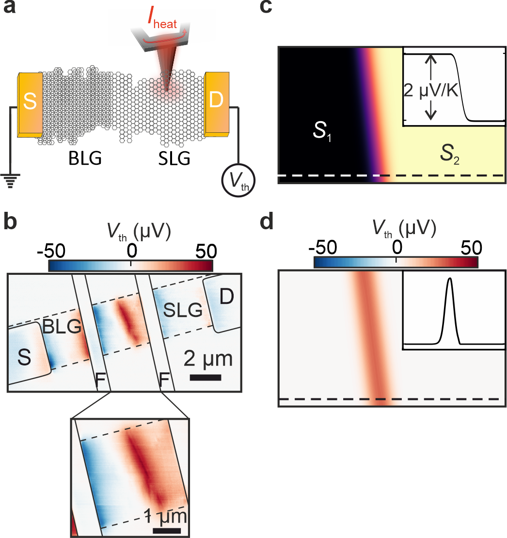
Our devices are made from exfoliated single-layer and bilayer graphene top contacted by Ti-Au contacts on a Si/SiO2 chip that serves as a global back gate (see methods for fabrication details). The measurements are performed employing a Scanning Thermal Microscope (SThM) setup, effectively an atomic force microscope (AFM) with a microfabricated resistor incorporated on the cantilever of the AFM probe close to the tip Gomès et al. (2015). When applying a high DC or AC voltage to the resistor the tip can be heated up by tens of Kelvin above the ambient SThM temperature and used as a local heat source. As this heat source is scanned over the sample with nanometer precision, the position dependent open-circuit voltage drop on the device is recorded (see Figure 1a for the measurement schematic) and in equilibrium no current is flowing in the sample.
STGM effectively presents a three terminal probing technique where heat from the STGM tip modifies the potential voltage drop across the two electrical terminals, producing a 2D nanoscale map of the thermoelectric response. Crucially, STGM does not require an electrical contact between the tip and the probed sample to measure the local thermoelectric response.
For a given Seebeck coefficient and a temperature increase caused by the tip , the tip position dependent thermovoltage can be written as (see SI)
| (1) |
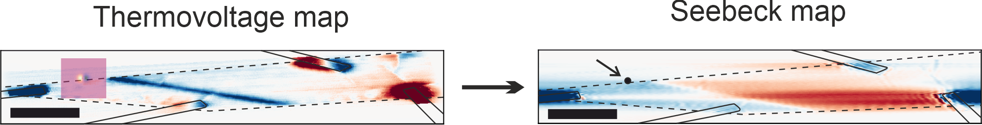
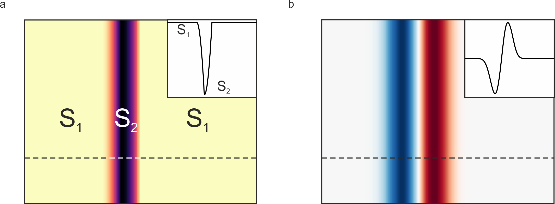
Here denotes the position of the tip, and the position of the left and right contact and the position dependent derivative of the temperature profile caused by the hot tip. Assuming that is a symmetric function, Equation (1) shows that reflects the local variations (asymmetry) of around within a length scale given by the thermal resistances of the sample. For a SLG/BLG junction for example, where symmetry is broken by the SLG/BLG step, we observe a positive thermovoltage signal at the junction when measuring the voltage drop at the SLG contact with the BLG contact grounded as shown in Figure 1b. The adjacent additional signal caused by the contacts will be discussed later. This positive thermovoltage signal can be explained by two different Seebeck coefficients in the single-layer and bilayer graphene area of the device, respectively, due to the different energy dispersion at low energies as previously reported Xu et al. (2010). Assuming a device where two materials with different Seebeck coefficients and are connected we can calculate the expected thermovoltage signal by convoluting with as shown in Equation (1). The difference in Seebeck coefficient V/K is displayed in Figure 1c. Here the temperature distribution is assumed to have a Gaussian shape see (Haché et al. (2012) and SI) and we convolute each line of the Seebeck map with the temperature distribution to obtain the thermovoltage map.
As can be seen in Figure 1d, the resulting thermovoltage signal is positive along the position of the junction where the BLG changes to SLG, reproducing the experimentally observed results well. We note that the width of the thermovoltage peak in the thermovoltage map is given by the length scale on which the change in Seebeck coefficient from to happens, and the width of the temperature distribution (see SI). As discussed later, it is possible to extract the width of the temperature distribution from the thermovoltage maps, which yields information about the band bending when changing the graphene thickness.
I.1 Rectangular Graphene Device
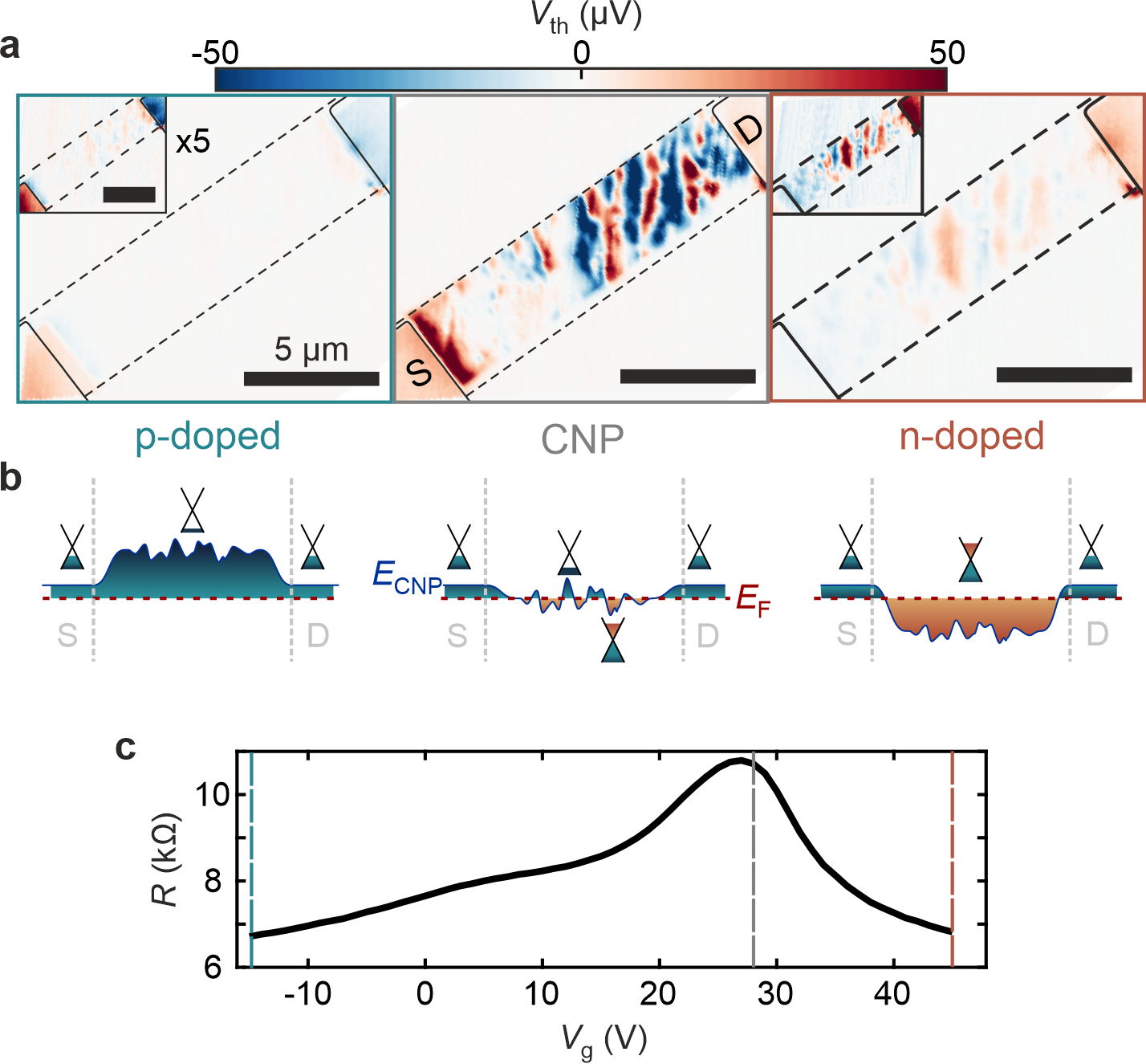
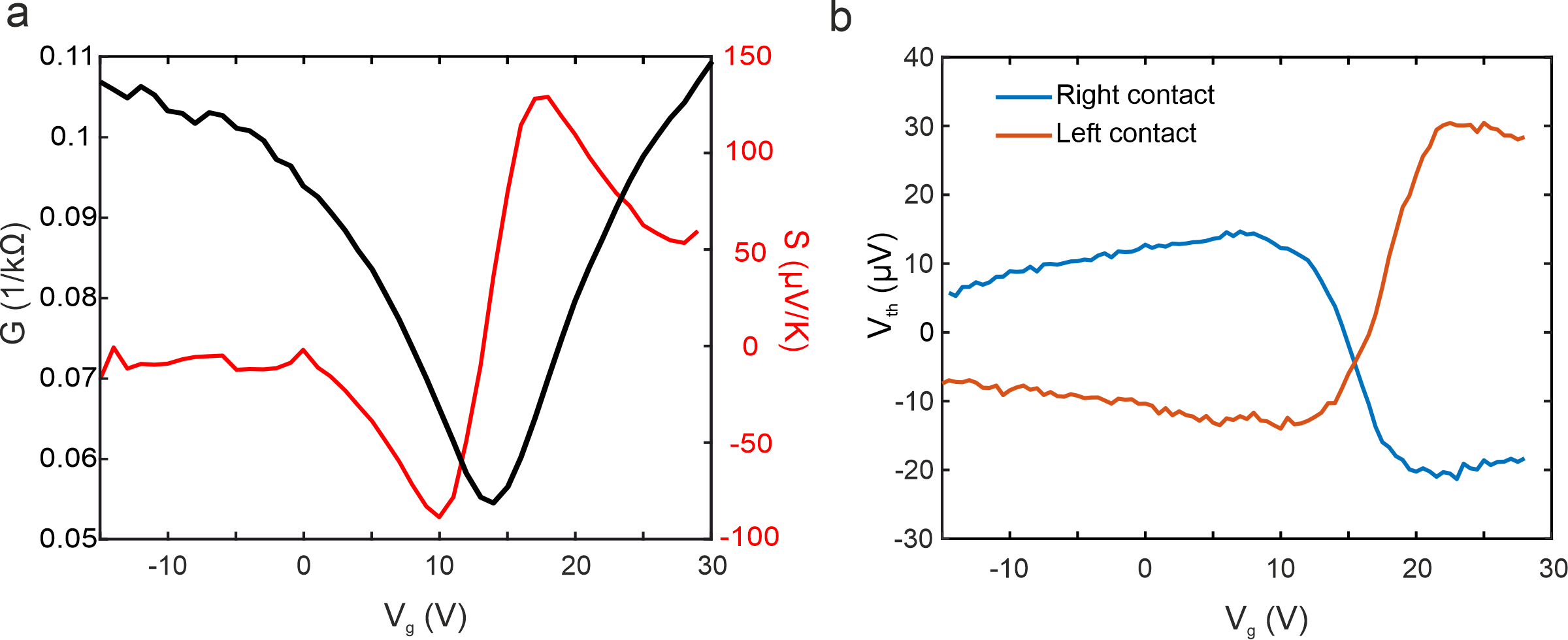
We first measure the gate dependent local thermoelectric signal of a graphene rectangle (see Figure 2). The charge neutrality point of the sample is at a back gate voltage of around V, as inferred from the gate dependent measurement of the two-terminal channel resistance (see Figure 2c). Thus, the graphene is strongly p-doped at V, which is due to the interaction of the SiO2 substrate surface charges with the graphene as reported previously Shi et al. (2009); Wang et al. (2012).
An STGM thermovoltage map with a tip apex-temperature of K is recorded at three back gate voltages: for a p-doped graphene channel at -15 V, close to the Dirac point at 28 V and for an n-doped graphene channel at 45 V (Figure 2a, left to right). The tip-apex temperature is defined with respect to the microscope stage and when the tip is in contact with the sample surface.
In the p-doped regime, a thermovoltage on the order of 30 V is generated across the device when the hot tip heats up the areas around the electrical contacts, where the polarity of the induced thermovoltage is negative (positve) when the source (drain) is locally heated up. As before, the source is defined as the contact kept on ground during the measurement. Only very little to no thermovoltage drop is observed when the tip is scanned over the graphene channel. At low carrier concentrations around the Dirac point, a seemingly chaotic distribution of thermovoltage signal of changing polarity appears in the graphene channel. In the n-doped regime, the signal along the graphene strip is again reduced. A larger voltage build up (compared to that in the channel) is observed when the source and drain contacts are heated up, with opposite polarity compared to the p-doped case.
The chaotic signal observed close to the Dirac point is attributed to charge puddles inside the graphene channel, which locally vary the energy dependent position of the charge neutrality point and are commonly observed for graphene on SiO2 substrates (see Figure 2b) Woessner et al. (2016); Xue et al. (2011). This leads to sharp local variations in which in turn influences the thermovoltage signal. We note that the signal from the charge puddles dominates the map at the charge neutrality point. This is due to the high sensitivity of the magnitude and sign of the Seebeck coefficient on the carrier density around the Dirac point Woessner et al. (2016); Zuev et al. (2009), resulting in large differences in over the short distances associated with charge puddles.
It is important to note, that a change in the thermal spreading resistance of the sample and the tip-sample interface thermal resistance, which is dominated by the thermal conductivity of the measured surface, strongly influences the tip-apex temperature. This is particularly relevant when the hot tip is in contact with the Au electrodes since the thermal conductivity of Au is two orders of magnitude larger than that of SiO2/graphene on SiO2. This leads to a reduction of the excess tip-apex temperature from K to K when the tip is in contact with Au compared to SiO2/graphene Tovee et al. (2012).
In the following we discuss the origin of the observed thermovoltage signals. When the hot tip heats up the left or right electrical contact, the measured thermovoltage drop corresponds to the sum of the thermoelectric voltage build-up of the graphene under the Au contacts and the graphene channel. This signal will later be used to estimate the (global) Seebeck coefficient of the graphene channel with respect to the graphene underneath the contact Xia et al. (2009).
The origin of thermoelectric signals is the preference of charge carriers to diffuse from hot regions in a material towards colder regions. The driving force for this process is proportional to the temperature difference and the entropy the system gains per diffusing carrier. The latter is highest if a carrier diffuses towards regions of higher DOS. This, depending on the source/drain configuration and the majority carriers in the sample, results in the build up of a positive or negative thermovoltage under open circuit conditions.
Graphene underneath the gold contacts is shielded from the electric field created by a gate voltage, such that its carrier concentration is not affected when a is applied.
For a gate voltage V, where the graphene channel is highly n-doped (see Figure 2a right) the DOS at the Fermi energy is larger in the channel than in the graphene underneath the gold contact (see Figure 2b right), meaning electrons will diffuse from the contact area into the graphene channel. This results in a positive (negative) thermovoltage build up at the drain (source) contact. While the DOS in the channel is still larger in the channel than in the graphene underneath the gold contact for a p-doped sample (see Figure 2b left), the majority carriers are now holes, resulting in a negative (positive) thermovoltage build up at the drain (source) contact.
I.2 Single-layer/Bilayer Junction
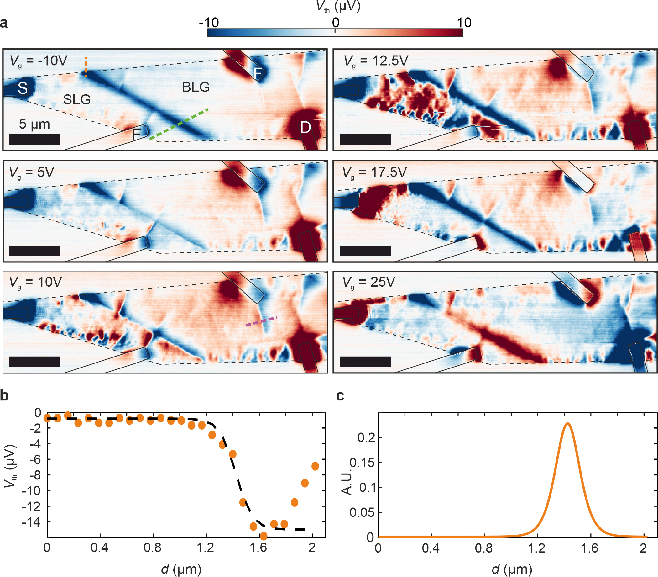
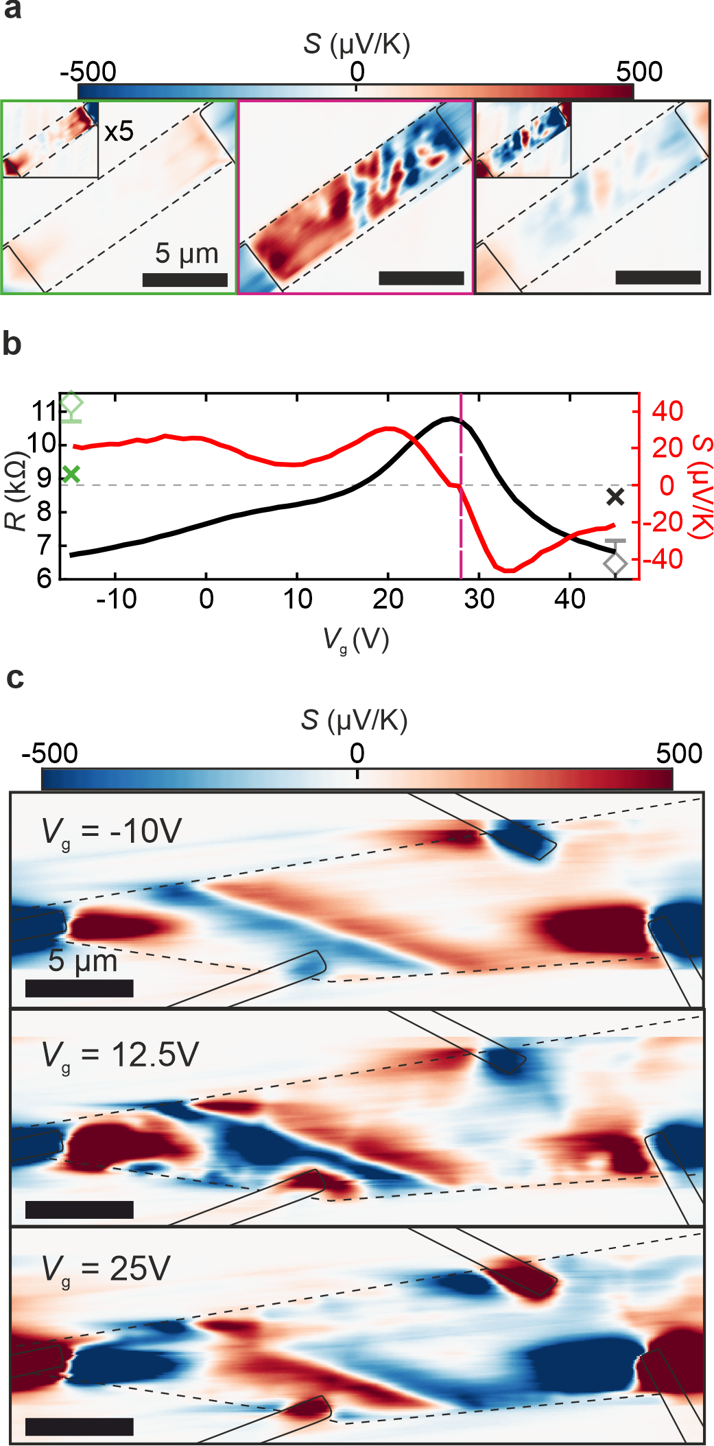
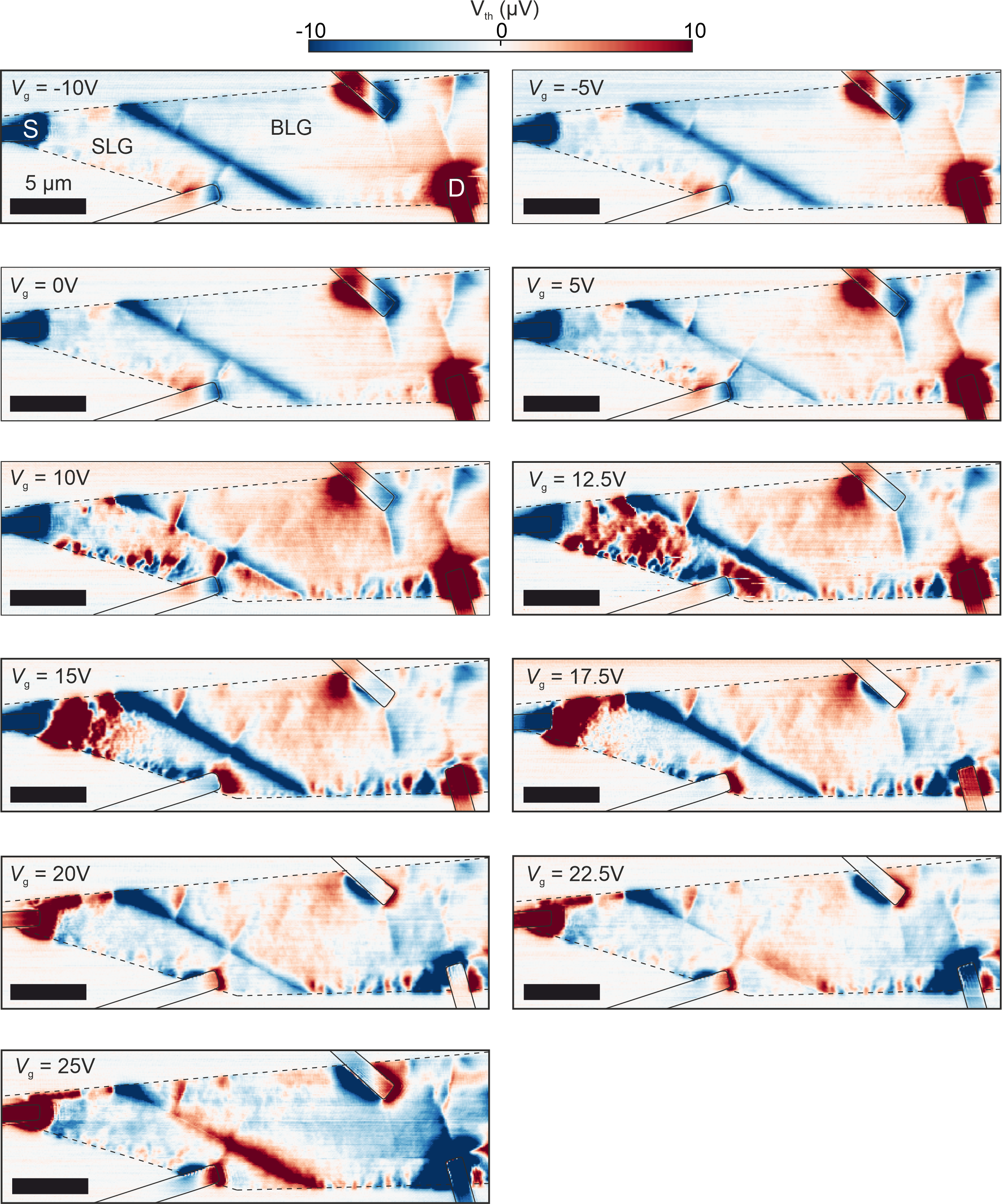
In the following, we apply STGM to a second type of graphene device, a junction formed between SLG and BLG (similar to the device and measurement shown in Figure 1b). Shown in Figure 3, the sample consists of a graphene flake that has both a single-layer and a bilayer section and is contacted by four gold contacts. The two contacts labelled source (S) and drain (D) are used for measuring the thermovoltage drop, while the other contacts are left floating (F).
In Figure 3, in accordance with the previous measurement of the graphene rectangle, a thermovoltage signal on the contacts is observed, which switches polarity as the gate voltage is swept over the charge neutrality point. The gate dependent thermovoltage maps highlight the impact of the contacts on the graphene sample.
The two passive, floating contacts show bi-polar signals, reversing polarity as the gate voltage is increased. This is because the floating contacts locally dope the graphene and pin the carrier density, an effect that has previously been observed in scanning photocurrent microscopy measurements Lee et al. (2008). In addition, the Fermi level pinning from the contacts leads to a strongly non-homogenous change of the carrier density within the sample. Rather than occurring simultaneously over the whole sample area, the change is gradual, starting from the SLG/BLG junction and wandering out towards the contacts as can be seen for higher gate voltages (right side of Figure 3 and further images in the SI).
Furthermore, STGM allows us to image the gate screening due to a second layer of graphene on top of the SLG channel. While a multitude of charge puddles appear around the charge neutrality point for gate voltages V on the SLG side, the BLG area of the sample shows hardly any. This is attributed to the electric field created by surface dipoles in the oxide being screened by the bottom layer and consequently not affecting charge carriers in the top layer, as previously indirectly observed Sun et al. (2010); Ohta et al. (2007). In addition, this observation provides evidence that the two graphene layers are thermally largely decoupled Rojo et al. (2019). Assuming charge puddles are present in the bottom layer as they are in the SLG area, any temperature differential caused by the tip should cause a thermovoltage signal, which is not observed in our experiment.
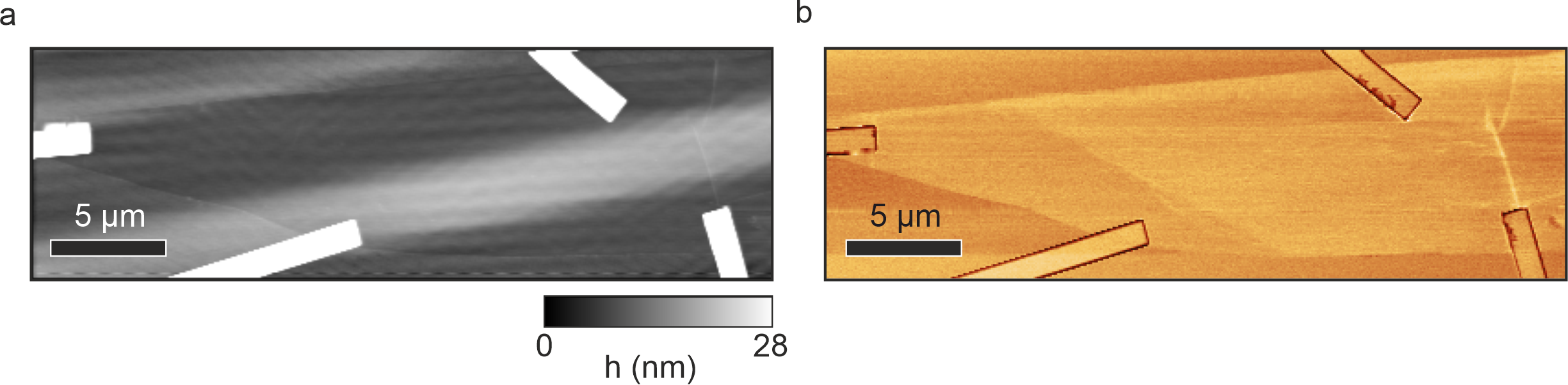
Furthermore, we observe thermovoltage signals along straight lines (one example is highlighted by a pink dashed line in the bottom left panel of Figure 3a) which are not visible in the height topography AFM maps (see SI). This signal could be attributed to local strain in the graphene layer or wrinkles, induced by the deposition of the contacts or the annealing step. Strain has been shown to alter the band structure Yoon et al. (2011) and Seebeck coefficient in graphene as well as displaying a Peltier effect Lu et al. (2020). Notably, at all gate voltages a strong thermovoltage signal is observed when heating up the interface between SLG and BLG as reported in scanning photocurrent measurements Mueller et al. (2009); Xu et al. (2010). The signal is changing from negative to positive as the gate voltage is increased. Both the wrinkle and the SLG/BLG junction signal follow a non-linear gate dependence.
The change in the sign at the SLG/BLG interface with changing majority carrier concentration (here both the SLG and BLG area of the sample is assumed to be p-doped (n-doped) for low (high) gate voltages respectively) implies that there is a change in the Seebeck coefficient difference .
As discussed above, diffusion of carriers is driven by a gain in entropy, and carriers diffuse from regions of low DOS into regions of high DOS. Due to the parabolic dispersion relation in BLG compared to the linear one in SLG around the charge neutrality point, the DOS in BLG is higher than in SLG McCann and Koshino (2013); Castro Neto et al. (2009). This leads to a positive (negative) thermovoltage build-up for electron (hole) doped graphene when measuring the voltage at the drain contact with respect to the source Xu et al. (2010). This development is shown in Figure 4a where line traces along the green dotted line in Figure 3a through the junction at different gate voltages are displayed. Figure 4b, top, shows close ups of the position dependent thermovoltage signal for a high p-doped ( V) and n-doped ( V) sample. For p-doped (n-doped) graphene, the signal dips (peaks) at the interface between SLG and BLG. Such a dip (peak) observed for the highly p-doped (n-doped) sample, respectively, is predicted by the model presented in Figure 1 and can be attributed to a step-wise change in the Seebeck coefficient between the SLG and BLG areas.
However, at gate voltages close to the charge neutrality point of the sample ( V) the thermovoltage exhibits a bipolar signal not compatible with a Seebeck coefficient changing from to . A similar bipolar signal at V is found around wrinkles as shown for an exemplary linecut in Figure 4c. Rather than indicating a transition from one Seebeck coefficient value to another, a bipolar signal implies a drop/peak of the Seebeck coefficient (see SI for simulations similar to the ones shown in Figure 1). For the wrinkles, the sudden spatial change in the Seebeck coefficient can be explained by local strain, which is the origin of the fold or wrinkle formation in the first place. It has been predicted that local strain in graphene can alter its Seebeck coefficient with the magnitude of this effect being largest around the charge neutrality point Nguyen et al. (2015). As a result, wrinkles in graphene exhibit a bipolar and prominent signal around the CNP. At higher doping, the change in the Seebeck coefficient is not as large and only leads to a small . While this describes the signal at the wrinkles, the nature of the bipolar thermovoltage displayed at the SLG/BLG junction is less clear. The bipolar thermovoltage could be a combination of the signal from charge puddles and the junction or be attributed to local symmetry breaking and disorder at the edges of the BLG which locally influences the Seebeck coefficient.
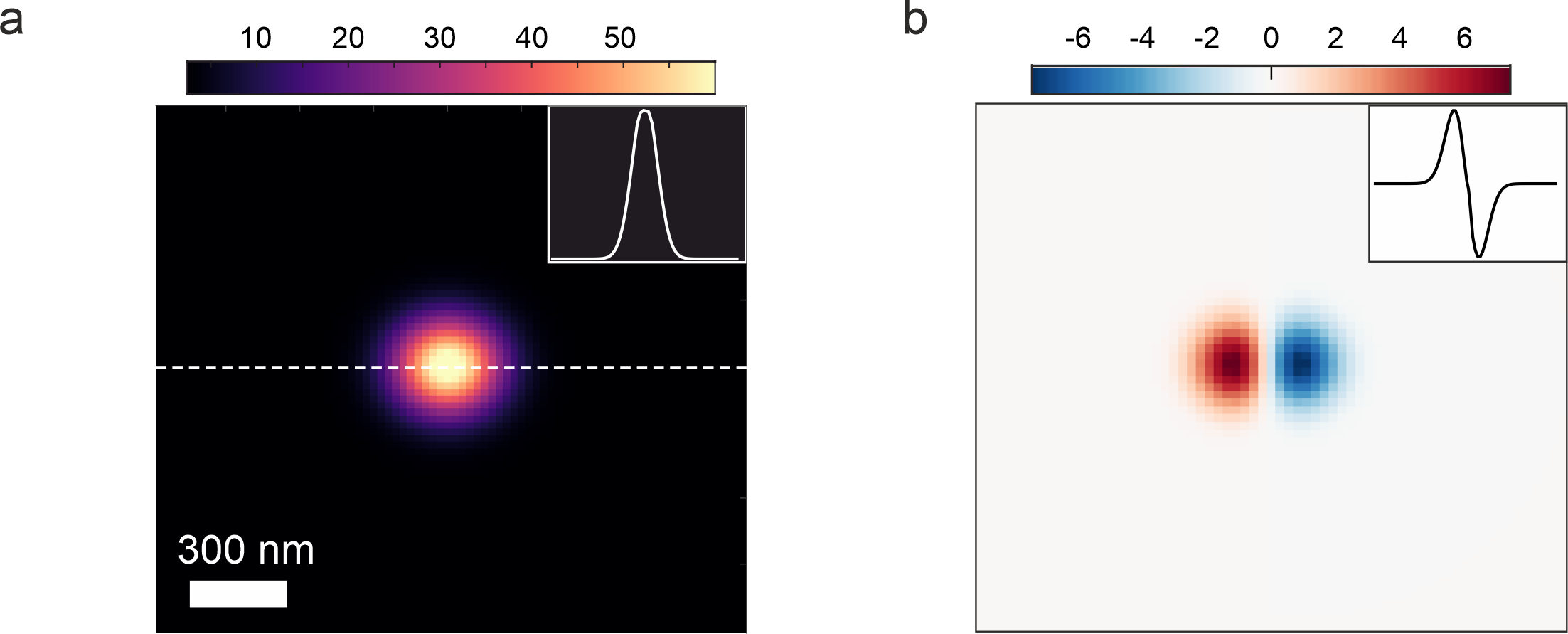
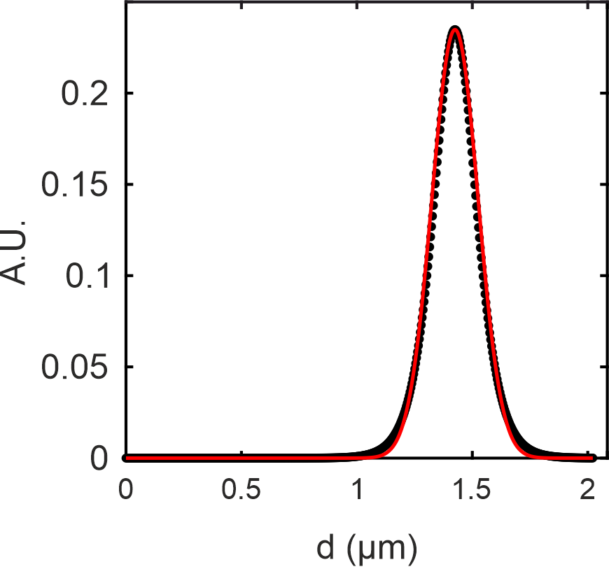
As explained above, the magnitude of the local thermovoltage signal measured by STGM is given by a convolution of a temperature difference with a given spatial Seebeck coefficient distribution. Thus it is possible to extract the length scales the Seebeck coefficient is changing on associated with the different origins of the signals. We note that the spatial distribution in the thermovoltage signals is directly influenced by two factors: the shape and height of the temperature profile distribution created by the STGM tip and the local changes of the Seebeck coefficient. In order to determine the width of the temperature distribution created by the STGM tip, we fit the step in the thermovoltage signal at the graphene flake edge with a sigmoidal Boltzmann curve (see orange dashed line in the top left pannel in Figure 3a and SI) Tovee et al. (2014). This fit gives nm, suggesting a lateral resolution of = 120nm. From this fit we can also extract a width of the Gaussian temperature distribution of m (see SI).
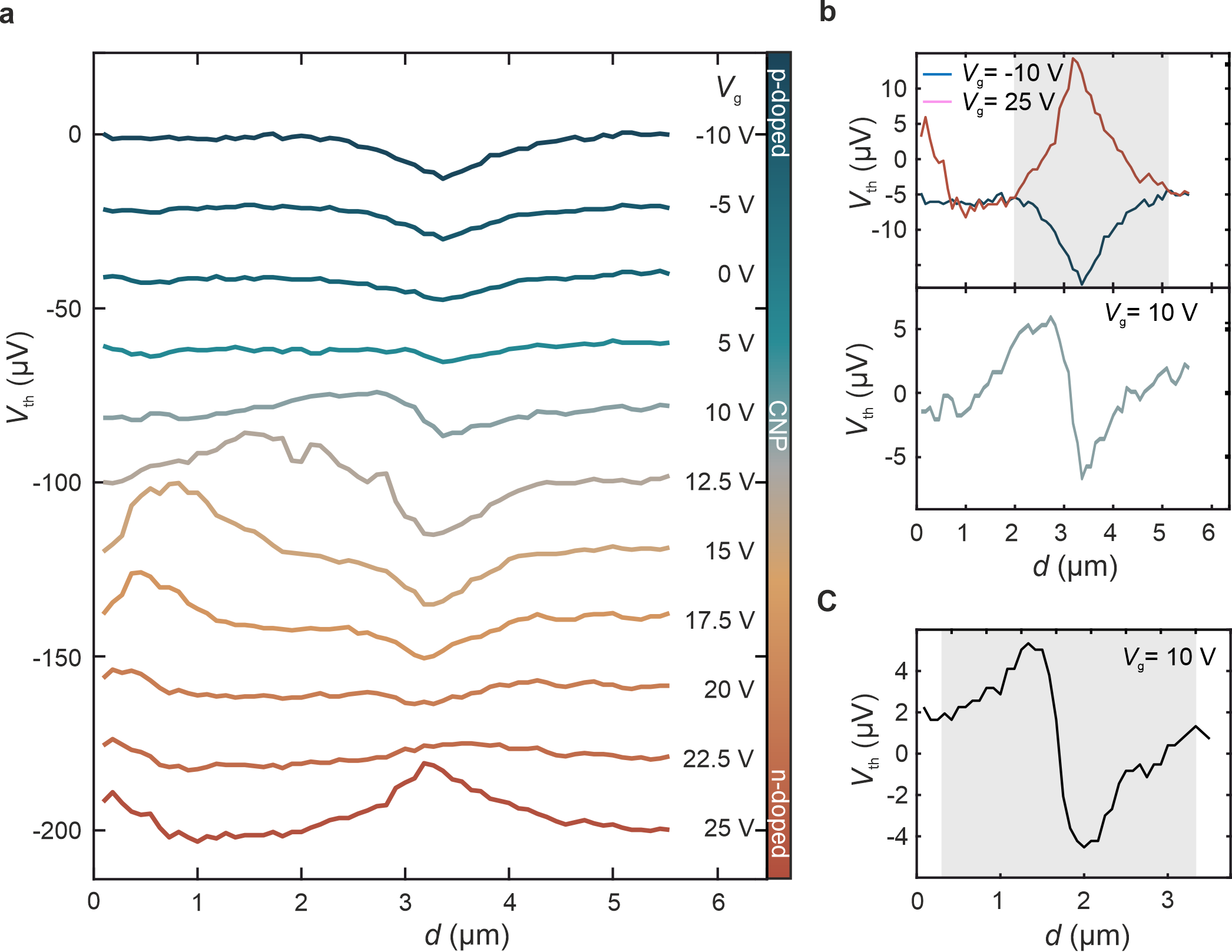
By comparing to the length scales observed in the experiment for the thermovoltage signal, m (see Figure 4b and c), it becomes clear that the width of the signal can not be explained by limited spatial resolution. Since the thermovoltage signal measured is a convolution of and , the signal width is approximately given by the sum of and (the length scale associated with changes in the Seebeck coefficient), making it possible to extract . The signal width can then be used to quantify the band bending at the transition between SLG to BLG (similarly to the depletion region width in a semiconductor p-n junction that is determined by doping levels and applied voltage). Applying this to the line traces shown in Figure 4a which show m, we can extract the length scale of the Seebeck coefficient transition when moving from SLG to BLG, giving 2 m for both a p-doped and an n-doped sample. We note that our results suggest that depends on the carrier density: by lowering the carrier density we find that decreases to 1 m at V (see Figure 4a and SI). It is worth to mention that, although the length scales on which the Seebeck coefficient changes around the SLG/BLG junction and a wrinkle are similar, the underlying mechanism for this length scale is different (see Figure 4b top and c). While around the junction depends on charge carrier density, for wrinkles in graphene is expected to depend more on the elastic properties of graphene. Thus the above analysis suggests that even for an atomically sharp step between two 2D materials, the Seebeck coefficient changes gradually on a length scale of micrometers.
I.3 Estimating the Seebeck coefficient
Following Equation (1), the local thermovoltage is a convolution of the local variation of the Seebeck coefficient and the temperature gradient induced by the STGM tip. Therefore it is possible to extract the local Seebeck coefficient variations from a measurement of the local thermovoltage by deconvolution. We test this idea by making the following assumptions: 1) we assume a Gaussian distribution of the temperature profile induced by the heated tip, with nm as extracted from the sigmoidal Boltzmann curve fit (see SI). 2) we assume a constant thermal spreading resistance and therefore a constant tip-apex temperature. The error making this assumption is low if only the graphene channel is investigated and contact areas are neglected. 3) the thermovoltage is measured between two sample contacts in the x-direction and therefore contributions in the y-direction can be neglected (here we rotate the thermovoltage maps before performing the deconvolution).
From Equation (1) we know that is the convolution of and the position dependent derivative of the temperature profile caused by the hot tip , i.e. . Using the temperature distribution , and thereby , we can then deconvolute Equation (1) and obtain an estimate of the Seebeck coefficient distribution along the sample, (see SI). Using a regularized filter in combination with a constraint least-square restoration algorithm to perform the 1D deconvolution, a quasi two-dimensional temperature distribution is line-by-line deconvoluted with the thermovoltage map to produce the Seebeck map (see methods and SI).
As the tip is moved over the sample, the centre of its two-dimensional temperature distribution moves as well. Then, at every point of the thermovoltage map, a complete deconvolution of each line in the temperature distribution with the thermovoltage image gives a point in the deconvolution image.
The resulting deconvolution is shown in Figure 5a. First, we note that the signal on and around the contacts is not accurate as we assumed a constant excess temperature of the tip-sample contact (of 53 K) for the deconvolution. This is not given on the Au contacts where the tip-sample contact temperature drops substantially as discussed earlier. Therefore, the areas of the Au contacts, which effectively show the difference in Seebeck coefficients between gold and graphene Vera-Marun et al. (2016), do not necessarily have the right magnitude (see discussion below). The graphene channel in between the contacts however, satisfies assumption 2 and displays the expected change in the Seebeck coefficient from positive to negative with increasing gate voltage Zuev et al. (2009). In addition, large local variations of the magnitude and sign of the local Seebeck coefficient are observed around the Dirac point (see Figure 5). These give rise to the thermovoltage signal shown in Figure 2a.
In order to evaluate the deconvolution method presented in this work, we can compare its result to the Seebeck coefficient of the graphene channel obtained via two additional methods: 1) using the gate dependent conductance data of the device and the Mott formula to estimate Zuev et al. (2009) and 2) estimating the temperature drop over the whole sample when the STGM tip heats up one electrical contact, and use . For case 1), the Mott formula is given by
| (2) |
where is the electron charge, the electrical conductance, the Boltzman constant and the operating temperature (see SI). The gate dependent Seebeck coefficient of the rectangular sample can then be calculated using the gatetrace from Figure 2c with the results of this calculation shown in Figure 5b. The calculated Seebeck coefficient overall first increases, changes sign when crossing the charge neutrality point, further decreases, and subsequently increases towards zero again. We observe maximum and minimum values of the Seebeck coefficient around = 30-40 V/K and = -40 to -50 V/K, respectively.
Then, for method 2), we divide the average thermovoltage value on the contacts in Figure 2a by the assumed temperature difference between the contacts ( 1.5 K as discussed) giving = 5.92 V/K and = -4.19 V/K for the Seebeck coefficient at low and high gate voltage respectively. The distribution of values of on the contacts is plotted in a bar graph and fitted with a multi peaked Gaussian to determine the most likely event with the error then given by the width of the Gaussian (see SI).
Lastly, the Seebeck coefficient obtained via the deconvolution is extracted from the graphene channel in the maps of the spatial distribution of the Seebeck coefficient in Figure 5a. Again, the values of in the channel are found by fitting the distribution with a multi peaked Gaussian to determine the most likely event with the error then given by the width of the Gaussian (see SI). This gives = 44.94 V/K and = -42.91 V/K for the p-doped and n-doped channel respectively. The result of the three different methods to obtain the Seebeck coefficient in the sample are shown in Figure 5b.
The values found for all methods are qualitatively on the same order, considering the assumptions necessary. In addition, all methods find the same trend of a reversal in sign when changing majority carriers as expected for graphene Zuev et al. (2009). Method 2), that is the Seebeck coefficient estimated via the thermovoltage drop, quantitatively differs most likely due to the large error in determining the temperature difference across the device from heating up one contact.
The deconvolution can also be applied to the more complex thermovoltage maps of the SLG/BLG sample (Figure 5c). Here, artefacts introduced by the changing tip-sample thermal resistance are clearly visible in the contact area. However, trends predicted by theory like the change in the Seebeck coefficient of the SLG area with respect to the BLG area are visible, with at V and at V Xu et al. (2010). In addition, again, a high local variation of with changing polarity can be seen around the charge neutrality point, caused by charge puddles. While the calculated Seebeck coefficients around 500 V/K may seem high for a graphene channel, we note that these are local variations due to local effects rather than representations of the global Seebeck coefficient.
II Conclusions
To summarize, we used STGM, a novel method to probe the local thermoelectric properties of two-dimensional and thin-film devices on a nanometre scale.
STGM is a mixed-physics approach where the voltage response on the two electrical terminals of the device is mapped as a function of the position and the temperature of the nanoscale probed scanned across the surface of the studied nanostructure.
We were able to investigate the thermoelectric fingerprint of charge puddles in graphene, resolve effects in our sample such as Fermi level pinning by the metallic contacts leading to non-homogenous carrier concentration distribution and reveal how the local carrier concentration changes when a gate voltage is applied. Furthermore, we find that strain strongly impacts the local Seebeck coefficient in single-layer and multilayer graphene sheets. The STGM method developed in this paper further allows us to obtain the local Seebeck coefficient through deconvolution with a good qualitative agreement between values obtained by deconvolution and theoretical prediction.
STGM provides valuable insights in the thermoelectric phenomena in two-dimensional materials by noninvasively studying planar junctions and the influence of local defects or metal contacts on the thermoelectric properties of the sample. STGM provides important insights leading to new strategies to increase the efficiency of thermoelectric devices and limit thermoelectric noise in electronic devices. STGM is not restricted to 2D materials but could also be applied to study the local thermoelectric properties around single molecule junctions or quantum dot devices Harzheim
et al. (2020b); Gehring et al. (2019, 2017).
III Experimental
Device Fabrication.
The devices were fabricated by exfoliating HOPG on top of a standard Si/SiO2 chip with a 300 nm oxide layer. Subsequently, if required, the graphene was patterned employing standard electron-beam lithography and then etched using oxygen plasma. Then, 1 nm Ti/50 nm Au contacts were deposited on top of the graphene and the final devices were annealed at 350 degree Celsius under a forming gas atmosphere for 30 minutes.
Scanning Thermal Gate Measurements.
The SThM is located in a high vacuum environment, prohibiting parasitic heat transfer as well as the formation of a water meniscus between the tip and the sample to achieve a better thermal resolution Menges et al. (2016); Kim et al. (2012). In our measurements, the spatial resolution is limited by the size of the tip–sample contact, which is on the order of tens of nanometers.
For the STGM measurements, the SThM tip is heated up by applying a high AC voltage of at a frequency of 91 kHz for the thermal conductance measurements with a 4 V DC offset to the temperature sensor. This causes Joule heating, which results in an SThM tip excess temperature of K at the interface with graphene on the SiO2/Si substrate (see Supporting Information). This local heat source is then scanned over the sample while the global voltage drop over the two contacts is measured with a SRS650 low-noise preamplifier and a SR560 high-impedance voltage preamplifier. The thermovoltage measurements do not require electrical contact between the tip and the sample, and thereby eliminate linked uncertainty, as well as requirements on the strength of the electrical tip–sample contact Lee et al. (2012). The SThM can also be used in a passive tip configuration with the temperature of the sample modified via cooling (heating) of the stage.
We calibrate the electrical power applied to the tip resistor as a function of temperature on a heated stage inside a high-vacuum chamber as described elsewhere Tovee et al. (2012); Evangeli et al. (2019). Crucially, here the tip apex temperature is a fraction of the cantilever temperature depending on the thermal conductivity of the material in contact (See SI for more details).
Offsets introduced by the amplifier are accounted for by subtracting the background signal far away from the sample from the whole map.
Deconvolution.
The Deconvolution is performed using a regularized filter algorithm rather than one based on the more straight forward polynomial division, as the latter can become numerically unstable for large denominator coefficients. The filter used is a constrained least-squares filter, which aims to minimize the difference between the ideal and the restored image while keeping the high frequency and thereby noise component to a minimum Hunt (1973); Lagendijk and Biemond (2009). The point-spread function used for deconvolution is the derivative of the Gaussian temperature distribution (Figure 3c and SI), and a Laplacian operator is used as the regularization operator to retain image smoothness.
Acknowledgements.
OVK achnowledges EU project QUANTIHEAT (Grant 604668), EPSRC project EP/K023373/1, UKRI project NEXGENNA and Paul Instrument Fund, c/o The Royal Society. P.G. acknowledges a Marie Skłodowska-Curie Individual Fellowship under Grant TherSpinMol (ID: 748642) from the European Union’s Horizon 2020 research and innovation programme. CE aknowledges a Marie Sklodowska-Curie Individual Fellowship under Grant NOSTA (ID: 704280) and EPSRC grant EP/N017188/1.References
- Zhang et al. (2014a) Q. Zhang, Y. Sun, W. Xu, and D. Zhu, Advanced Materials 26, 6829 (2014a), ISSN 15214095, URL http://doi.wiley.com/10.1002/adma.201305371.
- Crossno et al. (2016) J. Crossno, J. K. Shi, K. Wang, X. Liu, A. Harzheim, A. Lucas, S. Sachdev, P. Kim, T. Taniguchi, K. Watanabe, et al., Science 351, 1058 (2016), URL http://science.sciencemag.org.ezproxy.stanford.edu/content/351/6277/1058.abstract.
- Harzheim et al. (2020a) A. Harzheim, F. Koenemann, B. Gotsman, H. van der Zant, and P. Gehring, In print (2020a).
- Kraemer et al. (2008) D. Kraemer, L. Hu, A. Muto, X. Chen, G. Chen, and M. Chiesa, Applied Physics Letters 92, 243503 (2008), ISSN 00036951, URL http://aip.scitation.org/doi/10.1063/1.2947591.
- Xia et al. (2009) F. Xia, T. Mueller, R. Golizadeh-Mojarad, M. Freitage, Y. M. Lin, J. Tsang, V. Perebeinos, and P. Avouris, Nano Letters 9, 1039 (2009), ISSN 15306984, URL https://pubs.acs.org/doi/10.1021/nl8033812.
- Guo et al. (2018) S. Guo, K. Yang, Z. Zeng, and Y. Zhang, Physical Chemistry Chemical Physics 20, 14441 (2018), ISSN 14639076.
- Levander et al. (2011) A. X. Levander, T. Tong, K. M. Yu, J. Suh, D. Fu, R. Zhang, H. Lu, W. J. Schaff, O. Dubon, W. Walukiewicz, et al., Applied Physics Letters 98, 012108 (2011), ISSN 00036951, URL http://aip.scitation.org/doi/10.1063/1.3536507.
- Lyeo et al. (2004) H. K. Lyeo, A. A. Khajetoorians, L. Shi, K. P. Pipe, R. J. Ram, A. Shakouri, and C. K. Shih, Science 303, 816 (2004), ISSN 00368075.
- Zhang et al. (2010) Y. Zhang, C. L. Hapenciuc, E. E. Castillo, T. Borca-Tasciuc, R. J. Mehta, C. Karthik, and G. Ramanath, Applied Physics Letters 96, 062107 (2010), ISSN 00036951, URL http://aip.scitation.org/doi/10.1063/1.3300826.
- Sun et al. (2012) D. Sun, G. Aivazian, A. M. Jones, J. S. Ross, W. Yao, D. Cobden, and X. Xu, Nature Nanotechnology 7, 114 (2012), ISSN 17483395.
- Gabor et al. (2011) N. M. Gabor, J. C. Song, Q. Ma, N. L. Nair, T. Taychatanapat, K. Watanabe, T. Taniguchi, L. S. Levitov, and P. Jarillo-Herrero, Science 334, 648 (2011), ISSN 10959203.
- Zhang et al. (2014b) K. Zhang, F. L. Yap, K. Li, C. T. Ng, L. J. Li, and K. P. Loh, Advanced Functional Materials 24, 731 (2014b), ISSN 1616301X, URL http://doi.wiley.com/10.1002/adfm.201302009.
- Avsar et al. (2011) A. Avsar, T. Y. Yang, S. Bae, J. Balakrishnan, F. Volmer, M. Jaiswal, Z. Yi, S. R. Ali, G. Guöntherodt, B. H. Hong, et al., Nano Letters 11, 2363 (2011), ISSN 15306984, URL https://pubs.acs.org/doi/10.1021/nl200714q.
- Goossens et al. (2017) S. Goossens, G. Navickaite, C. Monasterio, S. Gupta, J. J. Piqueras, R. Pérez, G. Burwell, I. Nikitskiy, T. Lasanta, T. Galán, et al., Nature Photonics 11, 366 (2017), ISSN 17494893, eprint 1701.03242.
- Zuev et al. (2009) Y. M. Zuev, W. Chang, and P. Kim, Physical Review Letters 102 (2009), ISSN 00319007, eprint 0812.1393.
- Wei et al. (2009) P. Wei, W. Bao, Y. Pu, C. N. Lau, and J. Shi, Physical Review Letters 102 (2009), ISSN 00319007.
- Woessner et al. (2016) A. Woessner, P. Alonso-González, M. B. Lundeberg, Y. Gao, J. E. Barrios-Vargas, G. Navickaite, Q. Ma, D. Janner, K. Watanabe, A. W. Cummings, et al., Nature Communications 7 (2016), ISSN 20411723, eprint 1508.07864.
- Shiau et al. (2019) L. L. Shiau, S. C. K. Goh, X. Wang, M. Zhu, C. S. Tan, Z. Liu, and B. K. Tay, IEEE Transactions on Nanotechnology 18, 1114 (2019), ISSN 19410085.
- Harzheim et al. (2018) A. Harzheim, J. Spiece, C. Evangeli, E. McCann, V. Falko, Y. Sheng, J. H. Warner, G. A. D. Briggs, J. A. Mol, P. Gehring, et al., Nano Letters 18, 7719 (2018), ISSN 15306992, URL https://pubs.acs.org/doi/10.1021/acs.nanolett.8b03406.
- Gomès et al. (2015) S. Gomès, A. Assy, and P. O. Chapuis, Scanning thermal microscopy: A review (2015), URL http://doi.wiley.com/10.1002/pssa.201400360.
- Xu et al. (2010) X. Xu, N. M. Gabor, J. S. Alden, A. M. Van Der Zande, and P. L. McEuen, Nano Letters 10, 562 (2010), ISSN 15306984, eprint 0907.3173, URL https://pubs.acs.org/doi/pdf/10.1021/nl903451y.
- Haché et al. (2012) A. Haché, P. A. Do, and S. Bonora, Applied Optics 51, 6578 (2012), ISSN 15394522.
- Shi et al. (2009) Y. Shi, X. Dong, P. Chen, J. Wang, and L. J. Li, Physical Review B - Condensed Matter and Materials Physics 79 (2009), ISSN 10980121.
- Wang et al. (2012) Q. H. Wang, Z. Jin, K. K. Kim, A. J. Hilmer, G. L. Paulus, C. J. Shih, M. H. Ham, J. D. Sanchez-Yamagishi, K. Watanabe, T. Taniguchi, et al., Nature Chemistry 4, 724 (2012), ISSN 17554330.
- Xue et al. (2011) J. Xue, J. Sanchez-Yamagishi, D. Bulmash, P. Jacquod, A. Deshpande, K. Watanabe, T. Taniguchi, P. Jarillo-Herrero, and B. J. Leroy, Nature Materials 10, 282 (2011), ISSN 14764660, eprint 1102.2642.
- Tovee et al. (2012) P. Tovee, M. Pumarol, D. Zeze, K. Kjoller, and O. Kolosov, Journal of Applied Physics 112, 114317 (2012), ISSN 00218979, eprint 1110.6055, URL http://aip.scitation.org/doi/10.1063/1.4767923.
- Lee et al. (2008) E. J. Lee, K. Balasubramanian, R. T. Weitz, M. Burghard, and K. Kern, Nature Nanotechnology 3, 486 (2008), ISSN 17483395.
- Sun et al. (2010) D. Sun, C. Divin, C. Berger, W. A. De Heer, P. N. First, and T. B. Norris, Physical Review Letters 104 (2010), ISSN 00319007.
- Ohta et al. (2007) H. Ohta, S. Kim, Y. Mune, T. Mizoguchi, K. Nomura, S. Ohta, T. Nomura, Y. Nakanishi, Y. Ikuhara, M. Hirano, et al., Nature Materials 6, 129 (2007), ISSN 14764660.
- Rojo et al. (2019) M. M. Rojo, Z. Li, C. Sievers, A. C. Bornstein, E. Yalon, S. Deshmukh, S. Vaziri, M. H. Bae, F. Xiong, D. Donadio, et al., 2D Materials 6, 011005 (2019), ISSN 20531583.
- Yoon et al. (2011) D. Yoon, Y. W. Son, and H. Cheong, Physical Review Letters 106 (2011), ISSN 00319007, eprint 1103.3147.
- Lu et al. (2020) H. Lu, P. K. Chu, and Z. An, Small p. 1907170 (2020), ISSN 1613-6810, URL https://onlinelibrary.wiley.com/doi/abs/10.1002/smll.201907170.
- Mueller et al. (2009) T. Mueller, F. Xia, M. Freitag, J. Tsang, and P. Avouris, Physical Review B - Condensed Matter and Materials Physics 79 (2009), ISSN 10980121.
- McCann and Koshino (2013) E. McCann and M. Koshino, Reports on Progress in Physics 76 (2013), ISSN 00344885, eprint 1205.6953.
- Castro Neto et al. (2009) A. H. Castro Neto, F. Guinea, N. M. Peres, K. S. Novoselov, and A. K. Geim, Reviews of Modern Physics 81, 109 (2009), ISSN 00346861, eprint 0709.1163.
- Nguyen et al. (2015) M. C. Nguyen, V. H. Nguyen, H. V. Nguyen, J. Saint-Martin, and P. Dollfus, Physica E: Low-Dimensional Systems and Nanostructures 73, 207 (2015), ISSN 13869477, eprint 1505.06474.
- Tovee et al. (2014) P. D. Tovee, M. E. Pumarol, M. C. Rosamond, R. Jones, M. C. Petty, D. A. Zeze, and O. V. Kolosov, Physical Chemistry Chemical Physics 16, 1174 (2014), ISSN 14639076.
- Vera-Marun et al. (2016) I. J. Vera-Marun, J. J. van den Berg, F. K. Dejene, and B. J. van Wees, Nature Communications 7, 11525 (2016), ISSN 2041-1723, URL http://www.nature.com/doifinder/10.1038/ncomms11525.
- Harzheim et al. (2020b) A. Harzheim, J. K. Sowa, J. L. Swett, G. A. D. Briggs, J. A. Mol, and P. Gehring, Physical Review Research 2, 013140 (2020b), eprint 1906.05401, URL http://arxiv.org/abs/1906.05401.
- Gehring et al. (2019) P. Gehring, M. Van Der Star, C. Evangeli, J. J. Le Roy, L. Bogani, O. V. Kolosov, and H. S. Van Der Zant, Applied Physics Letters 115 (2019), ISSN 00036951, eprint 1907.02815.
- Gehring et al. (2017) P. Gehring, A. Harzheim, J. Spièce, Y. Sheng, G. Rogers, C. Evangeli, A. Mishra, B. J. Robinson, K. Porfyrakis, J. H. Warner, et al., Nano Letters 17, 7055 (2017), ISSN 15306992, eprint 1710.08344, URL http://pubs.acs.org/doi/abs/10.1021/acs.nanolett.7b03736.
- Menges et al. (2016) F. Menges, P. Mensch, H. Schmid, H. Riel, A. Stemmer, and B. Gotsmann, Nature Communications 7, 10874 (2016), ISSN 20411723, URL http://www.nature.com/doifinder/10.1038/ncomms10874.
- Kim et al. (2012) K. Kim, W. Jeong, W. Lee, and P. Reddy, ACS Nano 6, 4248 (2012), ISSN 19360851, URL www.acsnano.org.
- Lee et al. (2012) B. Lee, K. Kim, S. Lee, J. H. Kim, D. S. Lim, O. Kwon, and J. S. Lee, Nano Letters 12, 4472 (2012), ISSN 15306984, URL http://pubs.acs.org/doi/10.1021/nl301359c.
- Evangeli et al. (2019) C. Evangeli, J. Spiece, S. Sangtarash, A. J. Molina-Mendoza, M. Mucientes, T. Mueller, C. Lambert, H. Sadeghi, and O. Kolosov, Advanced Electronic Materials 5, 1900331 (2019), ISSN 2199160X, URL https://onlinelibrary.wiley.com/doi/abs/10.1002/aelm.201900331.
- Hunt (1973) B. R. Hunt, IEEE Transactions on Computers C-22, 805 (1973), ISSN 00189340, URL https://ieeexplore.ieee.org/stamp/stamp.jsp?tp={&}arnumber=5009169.
- Lagendijk and Biemond (2009) R. L. Lagendijk and J. Biemond, in The Essential Guide to Image Processing (Elsevier Inc., 2009), pp. 323–348, ISBN 9780123744579.
SI: Direct Mapping of Local Seebeck Coefficient in 2D Material Nanostructures via Scanning Thermal Gate Microscopy
IV Thermovoltage gate dependence
In order to illustrate the gate dependence of the thermovoltage, another SLG graphene device with higher gate resolution is studied. Figure S1a shows the conductance gate trace of the device and the calculated Seebeck coefficient using the Mott formula from Equation (2) in the manuscript. In S1b the gate dependence of the thermovoltage is shown, exhibiting a clear change from positive to negative for one contact and vice versa for the other one. This lineshape matches previous measurements very well and indicates a change in the majority carrier as reflected in the conductance trace. We note, that the signals change sign at slightly different gate voltages (though both in the vicinity of the Dirac point shown in S1a), most likely due to slight variations in the gating of the graphene underneath the contacts.
V Temperature Tip calibration
The temperature of the tip apex is a fraction of the tip-resistor temperature due to the conical shape of the tip, its material and the material the tip is in contact with. For a low thermal conductivity material with poor heat dissipation the temperature at the tip-sample contact will be higher than for a material with a higher thermal conductivity. The tip apex temperature when in contact with different materials can be found in Tovee et al. (2012); Evangeli et al. (2019) as obtained by experiments and COMSOL simulations. For example, the temperature increase at the tip when in contact with gold (thermal conductivity of 310 W) is 3-5% of the heater temperature and for 300 nm of SiO2 (thermal conductivity of about 1 W) it is 80-85% of the heater temperature.
VI Pseudo 2D Deconvolution
In order to deconvolute the thermovoltage maps and extract the Seebeck coefficient, a pseudo 2D deconvolution is used. First, a 2D map of the assumed temperature distribution on the sample, a Gaussian function, is calulated (see Figure S2a).
In a second step, this temperature distribution is differentiated along the x-axis as shown in Figure S2b. The differentiation is along the x-axis since we align all thermovoltages such that the two measurement contacts are aligned along the x-axis. We then assume any distribution to the thermovoltage that is resulting from the temperature gradient in the y-direction does not contribute to the measured thermovoltage and is neglected in the following.
In order to calculate the 2D Seebeck coefficient, this temperature gradient is then transposed on top of part of the thermovoltage image, that is with each line corresponding to one line in the thermovoltage image (see Figure S3). Then each line of the temperature gradient image is deconvoluted with each line of the thermovoltage image in a 1D line convolution described in the methods and the result added up. Since here the middle of the temperature gradient image represents the position of the heated SThM tip, this gradient image is then scanned over the thermovoltage image, with each pixel in the resulting Seebeck picture corresponding to the deconvolution of the surrounding area around the respective pixel in the thermovoltage with the temperature gradient image.
The algorithm used here is deconvreg which is part of the Matlab image processing toolbox and uses a regularized filter algorithm. It assumes, that the image to be deconvoluted (the thermovoltage map) was created by convolving the original image (the Seebeck coefficient map) with a point spread function (the temperature profile of the SThM tip) and the addition of noise. Crucially, since this algorithm is developed for images, it does not take into account the dimension of the original image or the deconvolved image. We will examine below how to correct for this.
For two recorded images ( and ) that are physical fields (that is moving along the pixels in the x and y direction of the image is associated with a change in a physical quantity such as position), their deconvolution is again a physical field. The units of the deconvolution are then given by where is the dimension of the image area, usually square meters. The convolution can then be written as a discrete Riemann sum as
| (S1) |
where the dimensionality of the image is taken into account by , the area of one pixel. In digital image processing, the units of the image are often ignored (as is the case in our deconvolution algorithm), meaning the convolution in this case is just given by
| (S2) |
As a result, in order to arrive at the right expression for the deconvolution we have to take into account the dimensionality of the original image by multiplying our image by . The algorithm used here is essentially employing Fourier transforms to perform the deconvolution, that is the deconvolution is given by:
| (S3) |
where and are the Fourier transforms of and respectively and denotes the inverse Fourier transform. Since Fourier transforms and therefore its inverse obey linearity the deconvolution, taking into account the dimensionality via , is given by
| (S4) |
Therefore, we need to multiply the resulting deconvolved Seebeck map by , which is equal to 0.0022 for the device shown in Figure 2 and 0.0047 for the device shown in Figure 3.
VII Additional Thermovoltage measurements on the SLG/BLG device
Additional gate dependent thermovoltage measurements of the SLG/BLG device are shown in Figure S4 highlighting the gate dependent effects discussed in the main text. In particular, the gate dependent strongly non-homogenous change of the carrier density due to Fermi level pinning by the contacts is clearly visible, as is the BLG gate screening. Both effects gate dependency is further shown in a GIF.
VIII Additional simulations for a bipolar thermovoltage signal
In order to investigate the Seebeck coefficient distribution leading to a bipolar signal, a drop in the Seebeck coefficient is convoluted with the temperature distribution . The Seebeck coefficient is assumed to drop from to and rise again to (see Figure S5). This Seebeck map is then line by line 1D convoluted with the Gaussian temperature distribution to arrive at the thermovoltage map shown in S5b. We note that having a differing Seebeck coefficient on either side of the drop (that is rather than rising to after the drop, the Seebeck coefficient rises to ) does not change the bipolar nature of the resulting thermovoltage signal though it does impact the lineshape. Since the thermovoltage observed in this study is relatively symmetric we assume an approximately equal Seebeck coefficient on either side of the dip (peak) with respect to the height of the dip (peak).
IX Mott formula Evaluation
In order to numerically evaluate the Mott formula in Equation (2) the measured conductance is differentiated with respect to the gate voltage . In addition, we can write the last part as
| (S5) |
where is the gate voltage at the Dirac point, m/s is the Fermi velocity in graphene and the gate capacitance is aF/. The complete Mott formula used for the calculations is then
| (S6) |
This can be evaluated using only the conductance trace of the device.
X Wrinkles in graphene
Most of the wrinkles in graphene giving off a signal in the thermovoltage measurements can not be seen in the height/thermal conductance maps. However, some of the more prominent ones in the right side of the picture can be distingusihed in the thermal conductance map, serving as a confirmation that the bipolar thermovoltage signal is emerging from wrinkles (see Figure S7).
XI Approximation of width of temperature distribution
In order to estimate the temperature distribution created by the tip, the derivative of the sigmoidal Boltzmann curve in Figure 3c is fitted with a Gaussian. The Gaussian has the form
| (S7) |
where is the position of the peak of the gaussian distribution and is the standard deviation. The fit (see Figure S7) gives 100 nm which is then used to deconvolute the thermovoltage maps and calculate the Seebeck maps. In addition, a width of the temperature distribution of m can be extracted.
XII Extraction of average Thermovoltage and Seebeck coefficient from maps
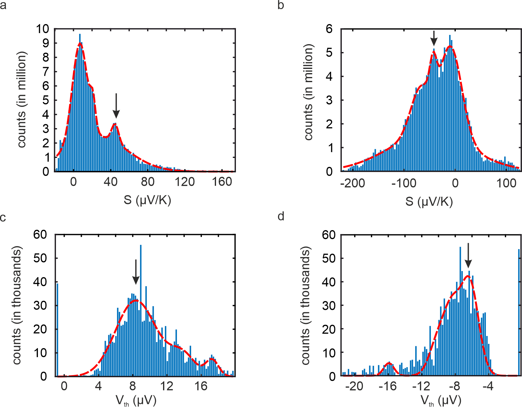
In order to extract the Seebeck coefficient of the graphene channel from the deconvoluted Seebeck maps in Figure 5a, the values in the channel are plotted in a bar graph (see Figure S7). We fit the distribution of values using a four peaked Gaussian to account for the multiple clusters clearly visible (see Figure S8. The clusters around a Seebeck coefficient of 0 V/K are attributed to charge puddles in the graphene that are still noticeable at high carrier concentrations. Similarly, small clusters at exceedingly high or negative are most likely due to effects near the contact and not chosen either. The peaks used are marked by a blac k arrow with the error being determined by the width of the respective peak. The same procedure was repeated for the thermovoltage but here, clear outliers in the thermovoltage values around 0 V/K were excluded.
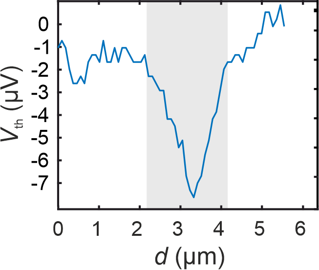
XIII Signal width at V
As can be seen in Figure S9, the width of the thermovoltage signal at V is approximately m. With m, we can estimate m.