The Sign of Three: Spin/Charge Density Waves
at the Boundaries of Transition Metal Dichalcogenides
Abstract
One-dimensional grain boundaries of two-dimensional semiconducting MX2 (M= Mo,W; X=S,Se) transition metal di-chalcogenides are typically metallic at room temperature. The metallicity has its origin in the lattice polarization, which for these lattices with symmetry is a topological invariant, and leads to one-dimenional boundary states inside the band gap. For boundaries perpendicular to the polarization direction, these states are necessarily 1/3 occupied by electrons or holes, making them susceptible to a metal-insulator transition that triples the translation period. Using density-functional-theory calculations we demonstrate the emergence of combined one-dimensional spin density/charge density waves of that period at the boundary, opening up a small band gap of eV. This unique electronic structure allows for soliton excitations at the boundary that carry a fractional charge of .
Introduction. The two-dimensional transition metal di-chalcogenides (TMDCs) MX2 (M= Mo,W; X=S,Se,Te), in their common -structure, are semiconductors with band gaps of 1-2 eV. Surprisingly, many edges and grain boundaries of these TMDCs are metallic at room temperature Bollinger et al. (2001). This seems to be true irrespective of the substrate on which the TMDC is deposited, or whether UHV conditions are used or not Ma et al. (2017a); Barja et al. (2016). Indeed, the exact atomic termination of edges and boundaries seems to be irrelevant for their metallicity Bollinger et al. (2003).
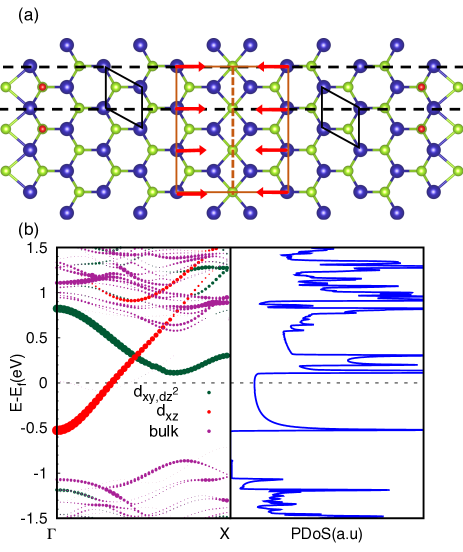
Experimentally, of the different possible TMDC edge configurations possible, mirror twin boundaries (MTBs) have been studied most extensively Batzill (2018); Ma et al. (2017a); Barja et al. (2016); van der Zande et al. (2013). MTBs occur spontaneously when TMDC monolayers are grown on isotropic substrates, or on substrates with a high in-plane symmetry, such as graphite. In essence, a MTB is formed between two TMDC crystallites that have their crystal growth directions rotated by 60 degrees, thereby forming mirror images of one another along the line of coalescence, see Fig. 1. MTBs are among the most predominant one-dimensional (1D) defects occurring during TMDC growth.
Whereas the presence of MTBs can be desirable or undesirable from the point of view of applications, the 1D metallic nature of the MTBs makes them interesting from a fundamental perspective. Two distinct views exist on the basic electronic structure of such MTBs. From angle-resolved photoemission (ARPES) results on monolayer MoSe2, the existence of a Tomonaga-Lüttinger liquid (TLL) has been put forward Ma et al. (2017b), which has also been claimed from scanning tunnelling microscopy and spectroscopy (STM, STS) on finite-length MTBs Jolie et al. (2019). In contrast, low-temperature STM and STS on the same material demonstrate the presence of a charge density wave (CDW) at the MTB with a wavelength of three lattice constants, opening up a band gap of eV Ma et al. (2017b); Barja et al. (2016).
Density-functional-theory (DFT) first-principles studies of MTBs have focused foremost on their atomic structure, and their stability and formation energies Lehtinen et al. (2015). There are several possible MTB structures, but overall the stoichiometric 44P structure, shown in Fig. 1, seems to occur most often experimentally Komsa and Krasheninnikov (2017); Barja et al. (2016). DFT calculations predict this structure to be metallic if a periodicity of one lattice constant along the MTB is assumed. Although it may appear likely that such 1D metallic structures are susceptible to CDW Peierls distortions Barja et al. (2016), so far, first-principles calculations have not been able to identify the presence of such structural distortions at MTBs, without resorting to artificial displacements of atoms.
In the present work, we analyze the electronic structure of 44P MTBs in MoSe2 and MoS2 monolayers. The metallicity is carried by 1D states localized at the MTB, where the intrinsic electric polarization of the 2D TMDC dictates a total occupancy of these states of per MTB lattice site. Including the spin degree of freedom, we show that a combined spin density wave (SDW) and charge density wave (CDW) at the MTB leads to a period tripling without structural distortion. The SDW/CDW lowers the total energy, and creates a band gap of a size comparable to experiment. The general mechanism proposed here not only holds for MTBs in MX2 (M= Mo,W; X=S,Se,Te), but also for edges with zigzag orientations Lucking et al. (2015), which are also commonly found in these materials. We speculate that this unique electronic structure allows for soliton excitations at such boundaries and edges that carry a fractional charge of Shin et al. (2012).
In our calculations we model MTBs in a periodic supercell geometry. The supercell typically contains a ribbon of twelve MX2 units across the -direction and a number of units along the -direction, with ribbons in neighbouring supercells separated by 10 Å vacuum in the and direction, see Fig. 1. Further computational details can be found in the Supporting Information 111 See Supporting Information for details on exchange-correlation functionals used and other DFT parameters, It includes the references Kresse and Furthmüller (1996); Kresse and Joubert (1999); Blöchl (1994); Hohenberg and Kohn (1964); Kohn and Sham (1965); Perdew and Zunger (1981); Dudarev et al. (1998) .
MTB states. The MX2 monolayer owing to its lack of inversion symmetry, has an in-plane electric polarization. Using the modern theory of polarization King-Smith and Vanderbilt (1993); Gibertini and Marzari (2015), it has been shown that the polarization of lattices with symmetry, such as the TMDCs discussed here, is a topological invariant Jadaun et al. (2013). symmetry only allows for polarizations with , where are the lattice vectors of the primitive 2D unit cell, and is one out of three possible values: , , or (hence, the topological invariant is ). Straightforward DFT calculations show that all our MX2 TMDCs belong to the same class and take on the specific value , see Fig. 1, which is in agreement with previous calculations Gibertini and Marzari (2015).
Crossing the MTB, the polarization is inverted (), see Fig. 1. This abrupt jump in the topological invariant causes the semiconducting band gap to close, and gives rise to metallic states Čadež et al. (2019). These localised interface states are responsible for compensating the line charge (, with the normal to the MTB) that originates from the polarization Güller et al. (2013). We stress that these are additional electronic gap states created as a result of the abrupt change of the topological invariant at the MTB, and not bulk bands pulled towards the Fermi level, as is sometimes argued to explain the metallic edges of a nanoribbon Gibertini and Marzari (2015); Güller et al. (2013), see Fig. 1. Indeed, similar states are found at edges modelled with a simple tight-binding model based on bulk parameters Farmanbar et al. (2016); Čadež et al. (2019).
A DFT calculation of the band structure of a MoSe2 MTB with the smallest possible periodicity, shows two bands, one partially occupied and the other completely empty, that lie within the band gap, see Fig. 1, in agreement with previous calculations Jolie et al. (2019). MTBs of other MX2 give similar band structures. On projecting on the atoms at the MTB, we find that one of these bands has mostly M character (shown in red in Fig. 1), whereas the other band has mostly M / character (highlighted in green).
The occupancy of these MTB states can be deduced from a simple general reasoning. As the polarization jumps from to going across the MTB, the result is a polarization line charge at the MTB (where is the lattice constant along the MTB). In a system that consists of macroscopic domains separated by MTBs, all of these boundaries have to be neutral, such as to avoid a polarization catastrophe Ohtomo and Hwang (2004). This means that each MTB must also carry an electronic charge , which compensates for the polarization charge. Such an electronic charge can only be carried by the 1D MTB interface states, located inside the band gap, as discussed above.
This means that these particular bands must have a total occupancy of electrons. Referring to Fig. 1, this results in the lower of the two bands being filled (accounting for spin degeneracy), whereas the upper one is completely empty 222Like in most DFT calculations, we model the MTB by a ribbon of a limited width. In such a geometry one can have a transfer of electrons between the (metallic) edges of the ribbon and the (metallic) MTB, in order to equilibrate the Fermi level. This can cause the occupancy of the MTB bands (and that of the edge bands) to deviate slightly from , as can be observed in Fig. 1. Although this is physical for a small ribbon, the electron transfer is artificial when the ribbon is used to model a single MTB. We suppress this artificial electron transfer by forcing the edges to be insulating, which can be done in a supercell with tripled periodicity, See Supporting Information.. Given their 1D character and the partial occupancy of , these metallic states might then be susceptible to a Peierls-type structural distortion that leads to a tripling of the period. However, like previous calculations, our DFT calculations do not give such a spontaneous structural distortion of the MTB Jolie et al. (2019); Barja et al. (2016).
SDW/CDWs. Nevertheless, it is highly unlikely that such 1D metallic states can escape electronic perturbations unscathed. We study the possibility of charge ordering and concomitant spin ordering using DFT+U calculations. The on-site electron-electron Coulomb interaction in 4d transition metal atoms (TMs), such as Mo, is supposed to be weaker than that in 3d TMs, and is thus often assumed to be negligible. Explicit calculations of the screened Hubbard in TMs Şaşıoğlu et al. (2011), and in TM oxides Vaugier et al. (2012), however show that the latter assumption is often not justified, and that a moderate value of eV for Mo 4d states is not unreasonable. The states at the 1D grain boundaries have predominant Mo d character, which, because of the 2D surroundings, one may expect to be relatively weakly screened. It is therefore appropriate to include the on-site Coulomb interaction.
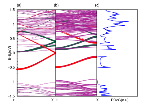
As a starting point, Fig. 2(a) shows the same MoSe2 band structure as in Fig. 1, but now in a cell, i.e., a cell that is tripled along the direction of the MTB. The Mo band (red) that was occupied in the simple unit cell, is now of course folded such, that the lowest branch is completely filled, and the upper two branches are completely empty. The Mo band (green) is also folded twice, but its three branches lie above the Fermi level. Using a Hubbard eV 333We use the rotationally invariant of the DFT+U functional, as formulated by Dudarev et al., where the Hubbard and exchange are combined into one parameter Dudarev., and re-optimizing the electronic structure Meredig et al. (2010), opens up a gap of eV between the filled and the empty states of the Mo band, as can be observed clearly in Fig. 2(b). The (empty) Mo bands change very little. The result is a band structure showing an indirect gap of eV between the occupied Mo band at X, and the unoccupied Mo band at . The corresponding DoS, shown in Fig. 2(c), shows this band gap, clearly marked by van Hove singularities characteristic of 1D structures. The emergence of this SDW decreases the total energy of the MTB by meV/ cell.
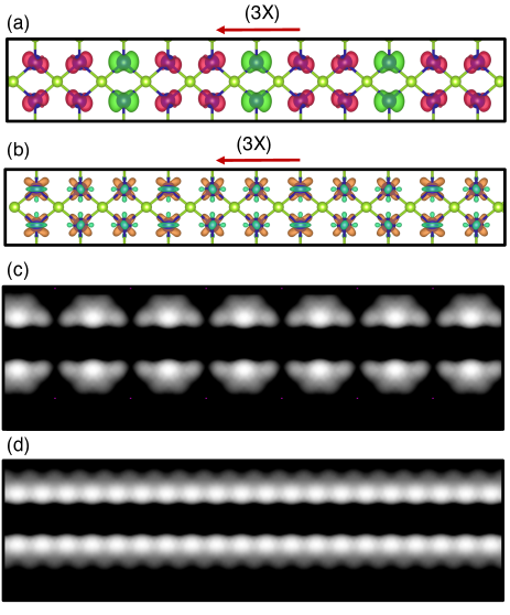
The origin of this band gap opening lies at the emergence of a SDW localized on the atoms closest to the MTB, which leads to magnetic moments on the three Mo atoms on one side of the MTB of , , and , respectively (the three Mo atoms on the other, the mirrored, side of the MTB have exactly the same magnetic moments). The inequivalence of the three Mo atoms is clearly visible in the spin density shown in Fig. 3(a). This SDW is accompanied by a quite subtle CDW, as shown in the corresponding local density of states (LDoS) in Fig. 3(b), which leads to a tripling of the period as observed in STM Barja et al. (2016), compare Fig. 3(c). Although we let the geometry of the MTB free to relax with the SDW/CDW, we observe no visible distortion in the structure. For instance, the bond lengths and bond angles between all atoms along the MTB remain the same. This means that the SDW/CDW is a purely electronic effect, and not a Peierls distortion.
MoS2 behaves similarly to MoSe2; in the 44P MTB structure of MoS2 a gap is opened by a SDW/CDW with periodicity. Using eV, the resulting magnetic moments on the Mo atoms closest to the MTB are , , and . The moments are somewhat smaller than for MoSe2, as is the induced gap at X. The resulting band structures in the gap region of MoS2 and MoSe2 are however quite similar, with MoS2 showing an overall indirect band gap of eV between the occupied Mo band at X, and the unoccupied Mo band at . The total energy of the MoS2 MTB is decreased by meV per cell., see Supporting Information.
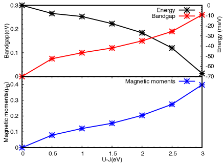
The onsite electron-electron Coulomb interaction is essential for the development of a SDW/CDW, i.e., in a calculation with it does not happen. Figure 4 shows the size of the band gap, the total energy decrease, as well as the size of the maximal magnetic moment on the Mo atoms at the MTB, as a function of the Hubbard value used in the calculation. It can be observed that both the band gap and the magnetic moments, increase monotonically with increasing , whereas the total energy decreases monotonically. All, however, remain sizeable even for relatively small values of , which indicates the robust presence of a SDW/CDW. Only if becomes smaller than eV, a SDW/CDW fails to develop.
Experimentally, the electronic structure of 44P MoSe2 MTBs has been interpreted using STM and STS in terms of CDWs by Barja et al. Barja et al. (2016), where they observed the characteristic periodicity. The observed band gap of eV suggest that the effective value of in their case is rather moderate, i.e., in the range 1-1.5 eV. Similarly, these CDWs have been seen in STM by Ma et al., and characterized by means of temperature-dependent conductivity measurements. We suggest that the CDW is accompanied by a SDW, which, although the magnetic moments are moderate, may be observed using spin-polarized STM.
Whereas the SDW/CDW should represent the ground state of the MTB, we cannot exclude that at a higher temperature, or for a markedly different MTB structure, electron correlations take over that are typical of 1D TLLs, as argued in Refs. Ma et al. (2017b); Jolie et al. (2019).
In the mean time, SDW/CDWs of periodicity allow for interesting soliton excitations, i.e., localized quasi-particles with fractional charges or , and spin , , or even an irrational number Su and Schrieffer (1981); Horovitz (1982). Such solitons will occur naturally on MTBs with an overall length that is not a mutiple of , because the boundary conditions at both ends of the MTB introduce frustration in the lattice Kim and Yeom (2012). In MTBs with lengths that are a multiple of , solitons do not exist in the ground state, but may be introduced by excitation. In particular, depositing TMDCs on substrates with which the electronic coupling is very weak, it may be possible to observe their fractional charges in a Coulomb blockade experiment, using STM, for instance.
In summary, using DFT+U calculations we have shown that a combined SDW and CDW of triple period arises in MTBs of TMDCs, which open up a band gap of eV in the 1D metallic band structure of a MTB. We argue that the triple period is necessarily the result of the topological invariant of these systems, i.e., the lattice polarization, which leads to metallic states in the 2D band gap, localized at the MTB, with a total occupancy of . The emergence of a SDW/CDW lifts the metallicity, but it also allows for topological soliton excitations, with charges that are multiples of .
References
- Bollinger et al. (2001) M. V. Bollinger, J. V. Lauritsen, K. W. Jacobsen, J. K. Nørskov, S. Helveg, and F. Besenbacher, One-dimensional metallic edge states in , Phys. Rev. Lett. 87, 196803 (2001).
- Ma et al. (2017a) Y. Ma, S. Kolekar, H. Coy Diaz, J. Aprojanz, I. Miccoli, C. Tegenkamp, and M. Batzill, Metallic twin grain boundaries embedded in mose2 monolayers grown by molecular beam epitaxy, ACS Nano, ACS Nano 11, 5130 (2017a).
- Barja et al. (2016) S. Barja, S. Wickenburg, Z.-F. Liu, Y. Zhang, H. Ryu, M. M. Ugeda, Z. Hussain, Z.-X. Shen, S.-K. Mo, E. Wong, M. B. Salmeron, F. Wang, M. F. Crommie, D. F. Ogletree, J. B. Neaton, and A. Weber-Bargioni, Charge density wave order in 1d mirror twin boundaries of single-layer , Nature Physics 12, 751 EP (2016).
- Bollinger et al. (2003) M. V. Bollinger, K. W. Jacobsen, and J. K. Nørskov, Atomic and electronic structure of nanoparticles, Phys. Rev. B 67, 085410 (2003).
- Batzill (2018) M. Batzill, Mirror twin grain boundaries in molybdenum dichalcogenides, Journal of Physics: Condensed Matter 30, 493001 (2018).
- van der Zande et al. (2013) A. M. van der Zande, P. Y. Huang, D. A. Chenet, T. C. Berkelbach, Y. You, G.-H. Lee, T. F. Heinz, D. R. Reichman, D. A. Muller, and J. C. Hone, Grains and grain boundaries in highly crystalline monolayer molybdenum disulphide, Nature Materials 12, 554 (2013).
- Ma et al. (2017b) Y. Ma, H. C. Diaz, J. Avila, C. Chen, V. Kalappattil, R. Das, M.-H. Phan, T. Čadež, J. P. Carmelo, M. C. Asensio, and M. Batzill, Angle resolved photoemission spectroscopy reveals spin charge separation in metallic mose2 grain boundary, Nature Communications 8, 14231 (2017b).
- Jolie et al. (2019) W. Jolie, C. Murray, P. S. Weiß, J. Hall, F. Portner, N. Atodiresei, A. V. Krasheninnikov, C. Busse, H.-P. Komsa, A. Rosch, and T. Michely, Tomonaga-luttinger liquid in a box: Electrons confined within mirror-twin boundaries, Phys. Rev. X 9, 011055 (2019).
- Lehtinen et al. (2015) O. Lehtinen, H.-P. Komsa, A. Pulkin, M. B. Whitwick, M.-W. Chen, T. Lehnert, M. J. Mohn, O. V. Yazyev, A. Kis, U. Kaiser, and A. V. Krasheninnikov, Atomic scale microstructure and properties of se-deficient two-dimensional mose2, ACS Nano, ACS Nano 9, 3274 (2015).
- Komsa and Krasheninnikov (2017) H.-P. Komsa and A. V. Krasheninnikov, Engineering the electronic properties of two-dimensional transition metal dichalcogenides by introducing mirror twin boundaries, Advanced Electronic Materials 3, 1600468 (2017).
- Lucking et al. (2015) M. C. Lucking, J. Bang, H. Terrones, Y.-Y. Sun, and S. Zhang, Multivalency-induced band gap opening at mos2 edges, Chemistry of Materials, Chemistry of Materials 27, 3326 (2015).
- Shin et al. (2012) J. S. Shin, K.-D. Ryang, and H. W. Yeom, Finite-length charge-density waves on terminated atomic wires, Phys. Rev. B 85, 073401 (2012).
- Note (1) See Supporting Information for details on exchange-correlation functionals used and other DFT parameters, It includes the references Kresse and Furthmüller (1996); Kresse and Joubert (1999); Blöchl (1994); Hohenberg and Kohn (1964); Kohn and Sham (1965); Perdew and Zunger (1981); Dudarev et al. (1998).
- Kresse and Furthmüller (1996) G. Kresse and J. Furthmüller, Efficient iterative schemes for ab initio total-energy calculations using a plane-wave basis set, Phys. Rev. B 54, 11169 (1996).
- Kresse and Joubert (1999) G. Kresse and D. Joubert, From ultrasoft pseudopotentials to the projector augmented-wave method, Phys. Rev. B 59, 1758 (1999).
- Blöchl (1994) P. E. Blöchl, Projector augmented-wave method, Phys. Rev. B 50, 17953 (1994).
- Hohenberg and Kohn (1964) P. Hohenberg and W. Kohn, Inhomogeneous electron gas, Phys. Rev. 136, B864 (1964).
- Kohn and Sham (1965) W. Kohn and L. J. Sham, Self-consistent equations including exchange and correlation effects, Phys. Rev. 140, A1133 (1965).
- Perdew and Zunger (1981) J. P. Perdew and A. Zunger, Self-interaction correction to density-functional approximations for many-electron systems, Phys. Rev. B 23, 5048 (1981).
- Dudarev et al. (1998) S. L. Dudarev, G. A. Botton, S. Y. Savrasov, C. J. Humphreys, and A. P. Sutton, Electron-energy-loss spectra and the structural stability of nickel oxide: An lsda+u study, Phys. Rev. B 57, 1505 (1998).
- King-Smith and Vanderbilt (1993) R. D. King-Smith and D. Vanderbilt, Theory of polarization of crystalline solids, Phys. Rev. B 47, 1651 (1993).
- Gibertini and Marzari (2015) M. Gibertini and N. Marzari, Emergence of one-dimensional wires of free carriers in transition-metal-dichalcogenide nanostructures, Nano Letters 15, 6229 (2015), pMID: 26291826, https://doi.org/10.1021/acs.nanolett.5b02834 .
- Jadaun et al. (2013) P. Jadaun, D. Xiao, Q. Niu, and S. K. Banerjee, Topological classification of crystalline insulators with space group symmetry, Phys. Rev. B 88, 085110 (2013).
- Čadež et al. (2019) T. Čadež, L. Li, E. V. Castro, and J. M. P. Carmelo, Robust one dimensionality at twin grain boundaries in , Phys. Rev. B 99, 155109 (2019).
- Güller et al. (2013) F. Güller, A. M. Llois, J. Goniakowski, and C. Noguera, Polarity effects in unsupported polar nanoribbons, Phys. Rev. B 87, 205423 (2013).
- Farmanbar et al. (2016) M. Farmanbar, T. Amlaki, and G. Brocks, Green’s function approach to edge states in transition metal dichalcogenides, Phys. Rev. B 93, 205444 (2016).
- Ohtomo and Hwang (2004) A. Ohtomo and H. Y. Hwang, A high-mobility electron gas at the laalo3/srtio3 heterointerface, Nature 427, 423 (2004).
- Note (2) Like in most DFT calculations, we model the MTB by a ribbon of a limited width. In such a geometry one can have a transfer of electrons between the (metallic) edges of the ribbon and the (metallic) MTB, in order to equilibrate the Fermi level. This can cause the occupancy of the MTB bands (and that of the edge bands) to deviate slightly from , as can be observed in Fig. 1. Although this is physical for a small ribbon, the electron transfer is artificial when the ribbon is used to model a single MTB. We suppress this artificial electron transfer by forcing the edges to be insulating, which can be done in a supercell with tripled periodicity, See Supporting Information.
- Şaşıoğlu et al. (2011) E. Şaşıoğlu, C. Friedrich, and S. Blügel, Effective coulomb interaction in transition metals from constrained random-phase approximation, Phys. Rev. B 83, 121101 (2011).
- Vaugier et al. (2012) L. Vaugier, H. Jiang, and S. Biermann, Hubbard and hund exchange in transition metal oxides: Screening versus localization trends from constrained random phase approximation, Phys. Rev. B 86, 165105 (2012).
- Note (3) We use the rotationally invariant of the DFT+U functional, as formulated by Dudarev et al., where the Hubbard and exchange are combined into one parameter Dudarev.
- Meredig et al. (2010) B. Meredig, A. Thompson, H. A. Hansen, C. Wolverton, and A. van de Walle, Method for locating low-energy solutions within , Phys. Rev. B 82, 195128 (2010).
- Momma and Izumi (2011) K. Momma and F. Izumi, VESTA3 for three-dimensional visualization of crystal, volumetric and morphology data, Journal of Applied Crystallography 44, 1272 (2011).
- Vanpoucke and Brocks (2008) D. E. P. Vanpoucke and G. Brocks, Formation of pt-induced ge atomic nanowires on pt/ge(001): A density functional theory study, Phys. Rev. B 77, 241308 (2008).
- Su and Schrieffer (1981) W. P. Su and J. R. Schrieffer, Fractionally charged excitations in charge-density-wave systems with commensurability 3, Phys. Rev. Lett. 46, 738 (1981).
- Horovitz (1982) B. Horovitz, Solitons in charge- and spin-density-wave systems, Phys. Rev. Lett. 48, 1416 (1982).
- Kim and Yeom (2012) T.-H. Kim and H. W. Yeom, Topological solitons versus nonsolitonic phase defects in a quasi-one-dimensional charge-density wave, Phys. Rev. Lett. 109, 246802 (2012).