Small Bragg-plane slope errors revealed in synthetic diamond crystals
Abstract
Wavefront-preserving x-ray diamond crystal optics are essential for numerous applications in x-ray science. Perfect crystals with flat Bragg planes are a prerequisite for wavefront preservation in Bragg diffraction. However, this condition is difficult to realize in practice because of inevitable crystal imperfections. Here we use x-ray rocking curve imaging to study the smallest achievable Bragg-plane slope errors in the best presently available synthetic diamond crystals and how they compare with those of perfect silicon crystals. We show that the smallest specific slope errors in the best diamond crystals (both freestanding or strain-free mounted) are about 0.15-0.2 rad/mm2. These errors are only a factor of two larger than the 0.05-0.1 rad/mm2 specific slope errors we measure in perfect silicon crystals. High-temperature annealing at 1450∘C of almost flawless diamond crystals reduces the slope errors very close to those of silicon. Further investigations are required to establish the wavefront-preservation properties of these crystals.
I Introduction
Diamond features a unique combination of outstanding physical properties perfect for numerous x-ray crystal optics applications where traditional materials such as silicon fail to perform. Diamond is a material of choice in applications requiring improved transparency to x-rays, highest x-ray Bragg reflectivity, thermal conductivity, mechanical stiffness, and resilience to radiation damage. Diamond optics are essential for tailoring x-rays to the most challenging needs of x-ray research. Diamond optics are becoming vital for generation of fully coherent hard x-rays by seeded x-ray free-electron lasers [see recent review paper Shvyd’ko et al. (2017) for details and references].
Progress in fabrication of synthetic high-quality diamond crystals has been substantial in the last two decades. Crystals with defect-free areas of mm2 and more grown by a temperature gradient method under high pressure and high temperature (HPHT) are now state of the art Burns et al. (2009); Polyakov et al. (2011); Shvyd’ko et al. (2011); Sumiya and Tamasaku (2012); Stoupin et al. (2016a). However, the perfection of diamond crystals is typically not as high as of silicon crystals, which are standard in x-ray crystal optics applications. In particular, the wavefront-preservation properties, critical for many applications, suffer from insufficient crystal quality.
Perfect crystals with flat Bragg planes are a prerequisite for wavefront preservation in Bragg diffraction. But nothing is perfect. How flat can Bragg crystal planes be in the best available diamond crystals? What are the smallest achievable Bragg-plane slope errors in the best presently available synthetic diamond crystals? How do these compare to those in perfect silicon crystals? These questions are addressed in the present paper.
In the studies presented in this paper, Bragg-plane slope errors are measured using x-ray Bragg diffraction rocking curve imaging (RCI), also known as sequential topography Lübbert et al. (2000). This technique is applied to best available diamond crystals featuring relatively large areas ( mm2) almost free of dislocations, stacking faults, inclusions, and other defects detectable by white beam x-ray topography Tuomi et al. (1974); Bowen and Tanner (1998), which is used to prescreen the diamond crystals. The Bragg-plane slope errors in diamond crystals are compared to those in highest quality reference silicon crystals.
We show that the smallest specific slope errors in the best diamond crystals are about 0.15-0.2 rad/mm2, which are only a factor of two larger than the rad/mm2 slope errors we measure in reference silicon crystals. Such small slope errors are achieved not only in freestanding diamond crystals but also in crystals firmly mounted in crystal holders, provided the crystals are designed and machined with special strain-relief features. High-temperature annealing at 1450∘C of the best diamond crystals further reduces Bragg-plane slope errors, such that hey approach those of silicon.
RCI data also provides access to the specific dispersion of the rocking curve widths . Normalized to the Bragg reflection width , it is a measure of the deviation from the largest Bragg reflectivity achievable by perfect crystals. The best diamond crystals feature normalized specific dispersion values 0.01-0.013/mm2 vs. 0.003-0.005/mm2 in silicon. These data indicates that the local reflectivity values in the best diamond crystals are reduced by not more than 1% to 1.3% from the maximum values, in agreement with previous Bragg reflectivity studies in diamond Shvyd’ko et al. (2011).
Further investigations are required to establish the wavefront-preservation properties of the best available diamond crystals.
The paper is organized as follows. In Section II we provide results of the RCI studies in a reference silicon crystal. Results of studies in selected freestanding diamond crystals and comparison with the reference silicon crystal are presented in Section III. Design, fabrication, and RCI studies of diamond crystals with strain relief features mounted in crystal holders are discussed in Section IV. Effects of high-temperature heat treatment on the Bragg-plane slope errors in diamond crystals are discussed in Section V. We refer to Appendix A for details on the RCI technique and to Appendix B for the methods of mitigating the impact of the beamline wavefront distortions on the actual values of the Bragg-plane slope errors. Appendix C provides details on high-temperature annealing.
II Bragg-plane slope errors in reference silicon
Prior to studying Bragg-plane slope errors in diamond crystal, we used the same RCI technique and setup (introduced in Appendix A) to measure RCI maps and the relevant crystal parameters in a specially prepared reference silicon crystal. These measurements were performed to establish a reference for the diamond crystals and to benchmark the ultimate performance of the RCI setup used in the later studies.
The reference crystal was manufactured from the highest quality high-resistivity single-crystal silicon, with the (531) crystal planes parallel to the surface. The 531 Bragg reflection is used to match the! 531 Bragg reflection from the conditioning crystal. The crystal was made relatively large (151515 mm2). Its lower part was fixed in a crystal holder in a manner that did not create strain in the upper part, which was exposed to x-rays.
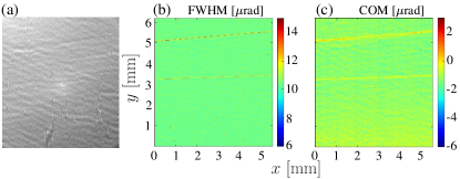
Figure 1(a) presents an x-ray image of our reference silicon crystal in the 531 Bragg reflection recorded at the crystal-integrated Bragg reflection rocking curve maximum [displayed in Fig. 11(a) of Appendix A]. Figure 1(b) shows a color map of the Bragg reflection angular widths (full width at half maximum, FWHM), while Fig. 1(c) shows a color map of the Bragg reflection peak relative angular positions , evaluated as a center of mass (COM) of the rocking curves. We note that the rippled background and the two straight lines in Figs. 1(a)-(c) are artifacts caused by beamline optical components (see Appendix B for more details).
The RCI data provide access to numerous crystal parameters that are calculated by the RCI data evaluation code. The parameters used in these studies and their definitions are summarized Table 1.
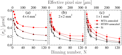
Of these parameters, Bragg-plane slope error is one of the most important in the present studies. Figure 2(a) shows values in the reference silicon crystal as a function of the binning number calculated in different regions of interest (ROI) indicated by appropriate colors in Fig. 2(c). The error bars represent variation of the values being averaged.
| Notation | Definition |
|---|---|
| Relative angular position of the Bragg reflection peak (center of mass, COM) measured at a particular location on the crystal by an area detector pixel. | |
| Bragg-plane slope error calculated as dispersion of the values within a selected region of interest (ROI) on the crystal. | |
| values averaged over multiple equal-size ROIs. | |
| , | Specific or values measured over mm2 ROIs. |
| Angular width (full width at half maximum, FWHM) of the Bragg reflection peak measured locally on the crystal by an area detector pixel. | |
| Dispersion of the values within an ROI. | |
| values averaged over several equal-size ROIs. | |
| , | Specific or values measured over mm2 ROIs. |
| =2.35/, =2.35/, etc | Normalized , , or values. |
| Data binning number. It is related to a method of adding (binning) the signal from adjacent area detector pixels together to achieve better signal-to-noise ratio or to minimize the effects of small observation errors at a cost of resolution. |
The binning procedure moderates the impact of imperfections in the beamline optics, as discussed in more detail in Appendix B. Remarkably, there is no significant change in the values measured in ROIs of different size, indicating a homogeneous quality of the reference silicon crystal and fairly flat crystal planes over relatively large crystal areas. The average specific Bragg-plane slope errors are rad/mm2. These numbers may not necessarily represent the true value of the Bragg-plane slope errors in silicon crystals. They might be even smaller. These numbers rather represent the resolution of our setup, limited by wavefront distortions in the beamline x-ray optical components.
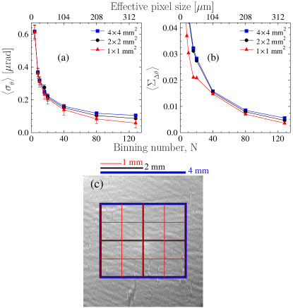
RCI data also provide access to the dispersion of the rocking curve widths . Normalized to the Bragg reflection width , it is a measure of the deviation from the largest Bragg reflectivity value for the given reflection. This can be easily understood, because the product of the Bragg reflection width and the reflectivity is an invariant value in the first approximation. Figure 2(b) shows a plot of the normalized and averaged Bragg width dispersion values (see Table 1 for the definition) in the reference silicon crystal as a function of the binning number calculated in ROIs of different size. Similar to the case of values in Fig. 2(a), there is no significant change in the values with the size of ROI. This is another indication of a very high and homogeneous quality of the reference silicon crystal. The specific average normalized Bragg width dispersion in silicon is 0.003-0.005/mm2. This is a small value, which indicates that the maximum Bragg reflectivity maybe reduced by less than 0.5% due to crystal strain. Similar to the case of , the small value of we measure in silicon may represent the resolution limit of the setup rather than the real value for single crystal silicon, which maybe even smaller.
III Bragg-plane slope errors in diamond crystals
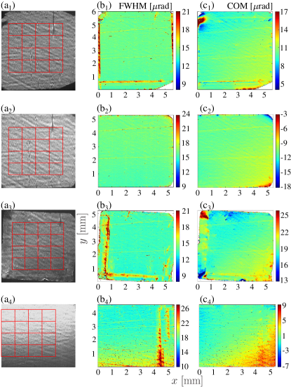
The studies of the Bragg-plane slope errors in diamond crystals were performed on samples selected using white-beam x-ray topography. All crystals are of type IIa grown by HPHT technique, cut and polished to plates in the (100) orientation Polyakov et al. (2011). Two of the available crystals (termed VB4 and VB5) feature large areas ( mm2) free of dislocations, stacking faults, inclusion, and other defects detectable by white beam x-ray topography. Crystal VB4 was used previously in diamond Bragg reflectivity studies Shvyd’ko et al. (2011). X-ray Bragg diffraction images and RCI maps of these two crystals are shown in the upper two rows of Fig. 3. The RCI maps are homogeneous in the central region, revealing in particular a Bragg reflection width of m close to the theoretical value. Another crystal (termed VB6) features a few weak dislocation lines in the central part. Stacking faults at the edges result is a propagating strain fields as well as areas with enlarged rocking curve widths clearly seen on the RCI maps in row 3 of Fig. 3. X-ray white-beam topography reveals more defects and propagating strain fields in a crystal labeled D3. The relevant RCI data in row 4 reveal crystal quality inferior to that of crystals VB4, VB5, and even VB6. All crystal plates are rather thick: crystal VB4 is 1 mm, while the others are about 0.5 to 0.6 mm thick.
To avoid any externally induced strain, which could be caused for example by crystal mounting, the crystals lie free in a flat 1-mm-deep indentation machined in an aluminum block fastened to the stage used to perform angular scans. The indentation holding the diamond crystal in it was covered with a thin plastic foil to minimize the effect of air circulation on the angular stability of the crystal.
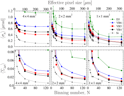
The upper row of Fig. 4 showns the averaged Bragg-plane slope errors measured and calculated in ROIs of different size for the four selected freestanding crystals. Data for the reference silicon crystal are also presented there for reference. The best crystal regions with the lowest density of defects are selected for this purpose, as indicated by red grids in Figs. 3(a)-(a). The smallest slope errors are observed as expected in crystals VB4 and VB5, in which the defects appear only on the crystal rims outside the selected ROIs. Unlike in silicon, slope errors in diamond crystals, even in the best crystals (VB4 and VB5), change substantially with the size of the ROI. This result indicates that the diamond crystal quality is less homogeneous than that of silicon.
Nevertheless, the averaged specific slope errors in the two best diamond crystals VB4 and VB5 (practically flawless in the central mm2 ROI) feature values 0.15-0.2 rad/mm2, only a factor of two larger than those in silicon. The overlapping error bars indicate that in some ROIs the specific errors in diamond and silicon are even comparable.
Similarly, the graphs in the lower row of Fig. 4 present plots of the averaged and normalized Bragg-reflection-width dispersions in the selected diamond crystals measured and calculated from the RCI data as a function of the area detector binning number . The values calculated in ROIs of various sizes are quite different, thus revealing again, in agreement with the values, more inhomogeneities in the diamond crystals than in the reference silicon crystal. Nevertheless, the specific values presented in the 11-mm2 graph can be small, especially for the highest quality crystals (VB4 and VB5), approaching 0.01-0.013/mm2, only a factor of two larger than the relevant reference silicon values.
This data indicates that the local reflectivity values in the two best diamond crystals are reduced (possibly by residual crystal strain) by no more than 1% to 1.3% from the maximum possible value. This result is in agreement with the direct absolute reflectivity measurements previously performed on crystal VB4 Shvyd’ko et al. (2011). The peak reflectivity measured with an x-ray beam having a 11 mm2 in cross-section and averaged over the central crystal area of 14 mm2 was 99.1%0.4%, which was close to the theoretical value of 99.7%. We note that the specific values presented here are evaluated on a larger crystal area of 4 mm2.
IV Impact of diamond crystal clamping
The data presented in the previous section were obtained on freestanding crystals. However, for optical components to function properly, they must be rigidly mounted in crystal holders to ensure angular and position stability. Correct mounting also provides for thermal transport to discharge the x-ray beam power absorbed by the crystal.
Even though the selected crystal plates are 0.5 to 1-mm thick and therefore very stiff due to the very large Young’s modulus of diamond, clamping without any precautions produce tremendous strain. A standard approach of reducing mounting strain is to introduce strain-relief features.
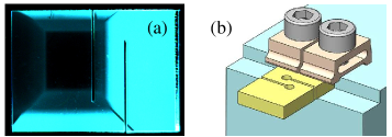
A high-quality type IIa HPHT 440-m-thick diamond crystal plate in the (100) orientation was selected, featuring a small amount of defects, mostly at the crystal rim. It was cut to a rectangular mm2 plate and furnished with strain relief cuts, as seen on a UV-excited luminescence image in Fig. 5. The darkest zone in the UV image corresponds to the (100) growth sector with lowest nitrogen content. The strain-relief cuts are the two vertical parallel dark lines. The cuts were introduced to prevent propagation of strain into the working area (on the left of left cut) provided the crystal is clamped rigidly on the right of the right cut. The cuts were made with YAG:Nd laser pulses in the 2nd harmonic with 100-ns duration, 1.7-mJ/pulse energy, spot size 20- to 25-m, and 5-kHz repetition rate. The width of the cuts is m, made in two passes with a 25-m lateral shift. Finite-element analysis shows that adding holes at the end of the cuts, as shown in Fig. 5(b), produces better strain relief; however, such holes were not implemented for this particular sample.
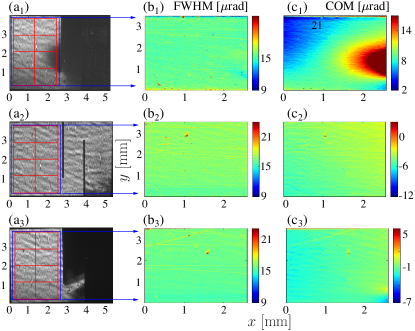
Figure 6(a) shows an x-ray 400 Bragg diffraction image at the top of the crystal integrated rocking curve. The image reveals that the laser cutting induces a very large strain: only the working area reflects x-rays and can be imaged. The rest of the crystal is out of reflection because of the cutting-induced strain. The FWHM map in the working area shown in Fig. 6(b) is very homogeneous, revealing almost theoretical Bragg reflection width, which proves almost defect-free crystal quality. However, the COM map presented in Fig. 6(c) reveals very large strain, in agreement with Fig. 6(a).
Is it possible to eliminate strain induced by laser cutting? In our previous studies Kolodziej et al. (2016) we found that annealing diamond crystals in air at a temperature of 630–650∘C for 3 hours may substantially reduce strain induced in the process of laser cutting or ablation. The strain is caused by the graphitization of the machined surfaces. The annealing temperature is chosen such that all residuals of graphite and other carbon compounds are burned in air, while keeping diamond intact111Increasing annealing temperature or time may result in etching of the crystal surface.. We will refer to this procedure in the following as medium-temperature in-air annealing (MTA).
Indeed, such annealing practically erases the cutting-induced strain as the x-ray Bragg diffraction image in Fig. 6(a) and RCI maps in Figs. 6(b)-(c) evidence. These measurements were performed on a free-standing crystal in the configuration previously described.
X-ray Bragg diffraction images and RCI maps in Figs. 6(a)-(c) show what happens to the crystal if it is rigidly clamped, as schematically presented in Fig. 5(b). At a first glance the image in Fig. 6(a) resembles the case of Fig. 6(a): only the working area can be imaged, while the rest is heavily strained and is out of reflection. In reality, the new situation is completely different. The COM map of the working area of the clamped crystal (on the left of the left cut) in Fig. 6(c) looks very similar to the COM map of the freestanding annealed crystal in Fig. 6(c). This demonstrates that clamping of a crystal furnished with strain-relief cuts does not produce strain in the working area.
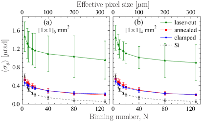
Averaged specific Bragg-plane slope error values presented in Fig. 7 support this statement. Both graphs show dependences on the binning number for the crystal after laser machining (green lines and markers), after MTA annealing (red), and clamped (blue). The averaging is performed either over six equal-size mm2 ROIs, shown in Fig.7(a) or over four such ROIs, shown in Fig.7(b). The ROIs are indicated by red grids in Figs. 6(a), (b), and (c), respectively. These data demonstrate that, first, annealing indeed helps to reduce substantially the slope errors to the values rad/mm2, which are very close to those observed for the best freestanding diamond crystals as documented in Fig. 4 (upper right graph). Second, and most important, the clamping does not degrade the observed slope errors in the upper working area. Extending averaging to all eight equal-size 1 mm2 ROIs results in an increase of (data not shown), indicating that the working area should be limited to the top 22 mm2 or at most to the 26 mm2 zone.
V Effect of high-temperature annealing
In the previous section it was shown that medium-temperature annealing at 630–650∘C of diamond crystals in air helps to erase crystal strain induced by laser machining and improve slope errors to the baseline values.
Here we study the effect of annealing diamond crystals at higher temperatures. Vacancies, impurity atoms such as nitrogen, and some other nanoscale crystal defects cannot be detected by x-ray topographies, but they still may contribute to the Bragg-plane slope errors. The mobility of vacancies, impurity atoms, and other defects increases at higher temperatures in condensed matter systems Cahn and Haasen (1996). The expectations are that in this process the defects may be pushed to the crystal surfaces and growth zone boundaries where they annihilate and reduce strain. In diamond such processes start at about 900∘C, but the highest temperature should be kept substantially lower than 2450∘C, the Debye-Waller temperature of diamond.
In our experiments, we anneal diamond crystals at 1450∘C for
3 hours under high-vacuum conditions ( mbar). We refer to this procedure as
high-temperature high-vacuum (HTHV) annealing;
Appendix C gives technical details.
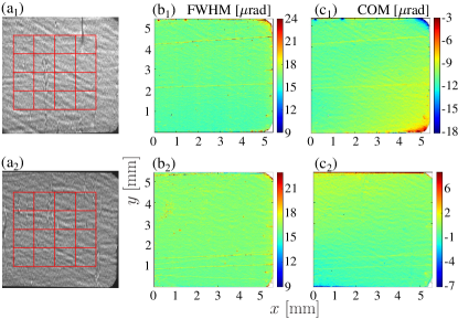
Figure 8 shows x-ray 400 Bragg diffraction images and RCI maps of diamond crystal VB5, one of the two best crystals used in these studies. The top row shows the results after MTA but before HTHV annealing, while the bottom row presents data after HTHV annealing. The upper row is the same as row 2 in Fig. 3. There is a clear improvement in the homogeneity of the COM map, indicating also reduction of the Bragg-plane slope errors .
Indeed the plots presented in Fig 9 support this assumption. Although there are still easy recognizable differences in the values calculated in ROIs of different size, the differences are not as large as before the HTHV annealing. The values after HTHV annealing approach the appropriate reference silicon values. Most striking, the averaged specific slope error values are reduced by almost a factor two to rad/mm2, becoming very close to the reference silicon value.
It is tempting at this point to make a general conclusion that the HTHV annealing improves substantially the Bragg-plane slope errors in diamond crystal and makes them close to those of silicon. This is most probably true if we are working with very high quality crystals like VB5. Unfortunately, this conclusion is not universally applicable. The HTHV annealing of diamond crystal VB6, which features some residual dislocation lines in the crystal center (in contrast to VB5, which is free of such defects), does not result in the same improvements as in the case of VB5. The very limited amount of high-quality samples available for our studies does not allow us to make a universal conclusion. As stated before, most probably, the HTHV annealing is efficient in improving Bragg-plane slope errors and pushing them to the silicon reference limit only in high-quality diamond crystals, that have no dislocations, no stacking faults, and so forth, in the region of interest. Improvements are likely due to annihilation of vacancies, impurity atoms, and so forth. These statements should be confirmed by studies on a larger set of high-quality diamond crystals.
VI Conclusions and outlook
Perfect crystals with flat Bragg planes are a prerequisite for wavefront preservation in Bragg diffraction. We use an x-ray rocking curve imaging technique to study the question of the smallest-achievable Bragg-plane slope errors in the best available synthetic diamond crystals and to compare them with those in highest quality reference silicon crystals.
We show that the smallest specific slope errors in the best diamond crystals are about rad/mm2, which are only a factor of two larger than the rad/mm2 slope errors we measure in reference silicon crystals.
RCI data also provides access to the normalized specific dispersion of the rocking curve widths , which is a measure of the deviation from the largest Bragg reflectivity achievable by perfect crystals. The best diamond crystals feature normalized specific dispersion values 0.01–0.013/mm2 vs. 0.003–0.005/mm2 in silicon. These data indicate that the local reflectivity values in the best diamond crystals are reduced by not more than 1% to 1.3% from the maximum values, in agreement with previous Bragg reflectivity studies in diamond Shvyd’ko et al. (2011).
The small slope errors are achieved not only in freestanding diamond crystals but also in crystals firmly mounted in crystal holders, provided the crystals are designed and machined with special strain-relief features.
High-temperature annealing at 1450∘C of the best diamond crystals may further reduce Bragg-plane slope errors to values approaching those of silicon.
Further investigations are required to establish the wavefront-preservation properties of the best available diamond crystals.
VII Acknowledgments
Dr. Stanislav Stoupin (Cornell High Energy Synchrotron Source, CHESS) is acknowledged for providing advanced RCI data evaluation codes for these studies. This material is based upon work supported by the U.S. Department of Energy, Office of Science, Office of Basic Energy Sciences Accelerator and Detector Research Program under Award Number DE-SC-PRJ1006724. Work at Argonne National Laboratory was supported by the U.S. Department of Energy, Office of Science, Office of Basic Energy Sciences, under contract DE-AC02- 06CH11357.
References
- Shvyd’ko et al. (2017) Yu. Shvyd’ko, V. Blank, and S. Terentyev, MRS Bulletin 62, 437 (2017).
- Burns et al. (2009) R. C. Burns, A. I. Chumakov, S. H. Connell, D. Dube, H. P. Godfried, J. O. Hansen, J. Härtwig, J. Hoszowska, F. Masiello, L. Mkhonza, et al., J. Phys.: Condensed Matter 21, 364224(14pp) (2009).
- Polyakov et al. (2011) S. N. Polyakov, V. N. Denisov, N. V. Kuzmin, M. S. Kuznetsov, S. Y. Martyushov, S. A. Nosukhin, S. A. Terentiev, and V. D. Blank, Diamond and Related Materials 20, 726 (2011).
- Shvyd’ko et al. (2011) Yu. V. Shvyd’ko, S. Stoupin, V. Blank, and S. Terentyev, Nature Photonics 5, 539 (2011).
- Sumiya and Tamasaku (2012) H. Sumiya and K. Tamasaku, Japn. J. Appl. Phys. 51, 090102 (2012).
- Stoupin et al. (2016a) S. Stoupin, S. Antipov, J. E. Butler, A. V. Kolyadin, and A. Katrusha, Journal of Synchrotron Radiation 23, 1118 (2016a).
- Lübbert et al. (2000) D. Lübbert, T. Baumbach, J. Härtwig, E. Boller, and E. Pernot, Nucl. Instrum. Methods Phys. Res. B 160, 521 (2000).
- Tuomi et al. (1974) T. Tuomi, K. Naukkarinen, and P. Rabe, Phys. Stat. Solidi (a) 25, 93 (1974).
- Bowen and Tanner (1998) D. K. Bowen and B. K. Tanner, eds., High Resolution X-ray Diffraction and Topography (Taylor and Francis, London, 1998).
- Kolodziej et al. (2016) T. Kolodziej, P. Vodnala, S. Terentyev, V. Blank, and Yu. Shvyd’ko, Journal of Applied Crystallography 49, 1240 (2016).
- Cahn and Haasen (1996) R. Cahn and P. Haasen, eds., Physical Metallurgy, vol. 1 (North Holland, 1996).
- Stoupin (2015) S. Stoupin (2015), URL https://www1.aps.anl.gov/science/scientific-software/dtxrd.
- Stoupin et al. (2016b) S. Stoupin, Yu. Shvyd’ko, E. Trakhtenberg, Z. Liu, K. Lang, X. Huang, M. Wieczorek, E. Kasman, J. Hammonds, A. Macrander, et al., AIP Conf. Proc. 1471, 050020 (2016b).
- Macrander et al. (2016) A. Macrander, M. Erdmann, N. Kujala, S. Stoupin, S. Marathe, X. Shi, M. Wojcik, D. Nocher, R. Conley, J. Sullivan, et al., in AIP Conf. Proc. (2016), vol. 1741, p. 030030.
Appendix A Rocking curve imaging
Bragg-plane slope errors in diamond and silicon crystals are measured using x-ray Bragg diffraction rocking curve imaging (RCI), also known as sequential topography Lübbert et al. (2000).
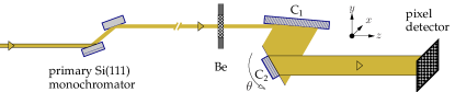
In this technique, a crystal under study is a second crystal (crystal C in Fig. 10) in a two-crystal nondispersive (or close to nondispersive) Bragg diffraction arrangement. The first (conditioning) crystal C is in a strongly asymmetric Bragg reflection geometry, with the asymmetry factor chosen such that x rays of each photon energy have a small angular spread upon Bragg reflection (here is an angular width of the symmetric reflection), much smaller than the Bragg reflection angular width of the second crystal . Such asymmetric reflection from the conditioning crystal also results in an increased cross-section of the reflected beam by a factor of , capable to illuminate the whole crystal C or its larger part. If the crystals are perfect, the Bragg reflection angular dependence (rocking curve) is very close to the intrinsic Bragg reflection angular dependence of the second crystal under study C. The conditioning crystal is typically manufactured from almost perfect silicon single-crystal material.
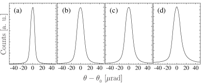
A pixel area x-ray detector is used to measure x-ray Bragg reflection images sequentially at different incidence angles of x-rays to the Bragg-reflecting atomic planes of the second crystal. Figures 1(a) and 3(a) show examples of such images measured in silicon and diamond crystals, respectively. They were recorded at the crystal-integrated Bragg reflection rocking curve peaks. Examples of crystal-integrated rocking curves are shown in Fig. 11. The procedure can be seen as measuring rocking curves at particular locations of the second crystal with the area detector pixels. The rocking curves measured with each detector pixel are used to calculate Bragg reflection maps. Figures 1(b) and 3(b) show examples of the color maps of the Bragg reflection angular widths (full width at half maximum, FWHM). Figures 1(c) and 3(c) show examples of the color map of the Bragg reflection peak relative angular positions , evaluated as a center of mass (COM) of the rocking curves. The RCI maps are calculated using a dedicated code Stoupin (2015). The microscopic structure defects can be derived from the Bragg reflection FWHM maps. The mesoscopic and macroscopic crystal strain and Bragg planes slope errors can be best evaluated from the COM maps.
We use an x-ray diffraction sequential topography setup Stoupin et al. (2016b) at x-ray optics testing beamline 1BM Macrander et al. (2016) at the Advanced Photon Source (APS). The setup enables rocking curve mapping with a submicroradian angular and 2.6-m spatial resolution. The latter is defined by a 6.5-m pixel size of ANDOR Neo-5.5 sCMOS camera and a 2.5 magnification of the collecting light optic.
We study in this paper diamond crystal plates in the (100) orientation using 400 Bragg reflection of 8-keV x-rays with Bragg’s angle . The expected in theory Bragg reflection width is rad (FWHM). Bragg reflection 531 from silicon with a Bragg’s angle for 8-keV x-rays (rad) is the best match for the closest-to-nondispersive double crystal setting with the 400 Bragg reflection from diamond. This reflection is used with the conditioning silicon crystal in the present studies. The crystal is asymmetrically cut with the asymmetry angle , resulting in the asymmetry parameter . The angular spread of monochromatic x-rays upon such Bragg reflection is rad, which is much smaller than .
The - and -axis in Figs. 1(a)-(c), 4(a)-(c), as well as in other x-ray Bragg diffraction images and RCI maps, correspond to the detector coordinates. The diffraction plane is parallel to the -axis. The x-ray Bragg diffraction images and RCI maps therefore appear to be contracted in the -direction by a factor of .
The examples presented in Fig. 1 are based on the measurements with a silicon crystal in the symmetric 531 Bragg reflection as the second crystal under study. Because Bragg reflections from both crystals are the same in this case, the crystals are in perfect nondispersive setting, with the rocking curves unaffected by the energy and angular spread of x-rays, predominantly determined by the Bragg reflection parameters of the second crystal. Both silicon crystals (conditioning and reference) were manufactured from highest quality (high-resistivity), almost perfect single-crystal material.
The measurements with silicon C crystal are performed to establish a reference for diamond crystals and to benchmark the ultimate performance of the RCI setup used in this studies. They are addressed in more detail in Section II.
Appendix B Moderating the impact of beamline wavefront distortions
As x rays propagating from the bending magnet source travel to the crystal under study they interact with numerous beamline optical components, including as Bragg-reflecting silicon crystals in the primary high-heat-load monochromator, two successive beryllium windows, and the conditioning crystal (see Fig. 10). Unfortunately, these interactions – and primarily with the two 0.25-mm-thick Be-windows – introduce significant wavefront distortions. The contrast observed on the x-ray Bragg diffraction images of the reference silicon crystal in Fig. 1(a), such as the rippled background and other irregular solitary features are due to the wavefront distortions and have nothing to do with the crystal imperfections. These distortions result in local fluctuations of the direction and of the angular distribution of the x rays incident on the crystal under study and therefore may perturb the local values of the Bragg reflection widths and peak positions , and therefore falsify genuine RCI maps and RCI characteristics. Indeed, the RCI maps in Figs. 1(b) and (c) inherit the rippled background structure of the x-ray Bragg diffraction image in Fig. 1(a). This of course affects the calculated RCI characteristic values, such as and , and may lead to false conclusions regarding crystal properties.
The distortions observed in Fig. 1(a) have a characteristic length from m to m. The characteristic length of the Bragg-plane slope variations in the defect-free regions are typically larger. Therefore, the negative impact of the wavefront distortions on the RCI maps and on the characteristic values can be mitigated by smoothing these distortions. A standard procedure in such cases is adding together (binning) the signal recorded by adjacent area detector pixels to achieve better signal-to-noise ratio and to minimize the effects of observation errors, albeit at a cost of resolution.
Figures 2(a) and 2(b) show plots of RCI characteristic values and , respectively, as a function of the binning number calculated in various crystal ROIs. The blue markers correspond to a mm2 crystal ROI. The black markers correspond to averaged RCI values calculated in four equal-size mm2 ROIs, while the red markers correspond to averaged RCI values calculated in sixteen equal-size mm2 ROIs. The error bars indicate the scattering range of the values we are averaging. The particular ROIs are indicated by appropriate colors in Fig. 2(c).
The RCI characteristic values and of the reference silicon crystal first decrees rapidly with and then reach steady values. The binning procedure minimizes the detrimental effect of the wavefront distortions due to the beamline optics. The genuine RCI characteristic values and of the reference silicon are close to those obtained with large binning numbers.
The binning procedure can “improve” the RCI characteristic values and only if the wavefront contrast in x-ray Bragg diffraction images is larger than the contrast due to crystal defects. If a crystal is damaged or badly strained the binning procedure cannot help. Figures 6(a)-(c) show an example of x-ray Bragg diffraction images and RCI maps of a diamond crystal significantly strained by laser machining. In this case binning cannot “improve” substantially the specific Bragg-plane slope errors , shown by green markers and lines in Fig. 7. The improvement in Bragg-plane slope errors occurs due to crystal annealing, as other data in Fig. 7 demonstrates.
Appendix C High-temperature high-vacuum annealing
A Red Devil G vacuum furnace manufactured by R.D. Webb Company Inc. was used for high-temperature high-vacuum annealing. Figure 12 shows typical temperature and pressure profiles in the furnace during the annealing process. The heating rate was 2∘C/min. The cooling rate was -3∘C/min. From 700∘C the heating was switched off and the furnace was allowed to cool naturally.
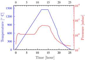
The vacuum is mbar at the beginning at room temperature, but it increases to mbar at 1450∘C. It is very important to have high-vacuum conditions to avoid diamond damage. However, even under such high-vacuum conditions the color of diamond changes to light gray. The subsequent medium-temperature annealing in air erases the gray color and makes diamond transparent again, suggesting that the color change is a surface rather than a bulk effect.