Gate tunable topological flat bands in twisted monolayer-bilayer graphene
Abstract
We investigate the band structure of twisted monolayer-bilayer graphene (tMBG), or twisted graphene on bilayer graphene (tGBG), as a function of twist angles and perpendicular electric fields in search of optimum conditions for achieving isolated nearly flat bands. Narrow bandwidths comparable or smaller than the effective Coulomb energies satisfying are expected for twist angles in the range of , more specifically in islands around for appropriate perpendicular electric field magnitudes and directions. The valley Chern numbers of the electron-hole asymmetric bands depend intrinsically on the details of the hopping terms in the bilayer graphene, and extrinsically on factors like electric fields or average staggered potentials in the graphene layer aligned with the contacting hexagonal boron nitride substrate. This tunability of the band isolation, bandwidth, and valley Chern numbers makes of tMBG a more versatile system than twisted bilayer graphene for finding nearly flat bands prone to strong correlations.
I Introduction
Van der Waals interfaces with small misalignment angles have emerged as a promising platform to study the correlated physics in layered materials where the low-energy bands are nearly flat due to extreme suppression of the Fermi velocities Hass et al. (2008); Miller et al. (2009, 2010); Sadowski et al. (2006); De Heer et al. (2010); Brihuega et al. (2012); Ohta et al. (2012); Lopes dos Santos et al. (2012, 2007); Shallcross et al. (2010, 2008); Landgraf et al. (2013); Shallcross et al. (2013); Bistritzer and MacDonald (2011); Moon and Koshino (2013, 2012); Jung et al. (2014); San-Jose et al. (2012); San-Jose and Prada (2013); Stauber et al. (2013); Bistritzer and MacDonald (2010); Wang et al. (2012); Schmidt et al. (2014); Carr et al. (2018); Koshino et al. (2018); Kang and Vafek (2019); Tarnopolsky et al. (2019); Po et al. (2019). Twisted bilayer graphene is the first representative system where the flatness of the bandwidth enhances the electron correlations leading to Mott-like insulating behaviors Cao et al. (2018a); Kim et al. (2017); Sharpe et al. (2019) and signatures of superconductivity Cao et al. (2018b); Yankowitz et al. (2019); Cao et al. (2020). A small twist angle of between the van der Waals interfaces generates a long periodic moire superlattice on the order of Å giving rise to a small mini moire Brillouin zone (MBZ) where the particles near the original Dirac points hybridize with each other through interlayer coupling Bistritzer and MacDonald (2011); Lopes dos Santos et al. (2012); Jung et al. (2014); Wong et al. (2015); Kerelsky et al. (2019); Choi et al. (2019). On the other hand, without any twist angle, moire superlattices are expected in graphene on hexagonal boron nitride (G/BN) van der Waals interfaces due to a lattice mismatch of 1.7 Yankowitz et al. (2012). The avoided gaps that appear at the Brillouin zone boundaries due to these moire potentials together with a bandgap opening near the charge neutrality point Song et al. (2015); Javvaji et al. (2020) is an effective way to obtain isolated low-energy flat bands that have well defined valley Chern numbers. Systems where a primary Dirac point gap opens under the effect of an electric field has realizations in rhombohedral trilayer graphene on hexagonal boron nitride (TG/BN) Chen et al. (2019a, b); Chittari et al. (2019); Zhang et al. (2019a) where the valley Chern number for either the valence or conduction bands are well-defined integers approximately proportional to layer number Chittari et al. (2019), and twisted double bilayer graphene (tDBG) Chebrolu et al. (2019); Liu et al. (2019a); Lee et al. (2019); Shen et al. (2020); Choi and Choi (2019); Koshino (2019); Li et al. (2019a) whose low energy bands assume valley Chern numbers range up to depending on the system parameters and their bandwidths are reduced roughly by a factor of two when compared to twisted bilayer graphene (tBG) Chittari et al. (2018); Chebrolu et al. (2019). When the valley degeneracy is lifted and occupancy is polarized Chittari et al. (2019); Zhang et al. (2019a, b); Bultinck et al. (2020) we can expect the onset of spontaneous quantum Hall phases even in the absence of magnetic fields Haldane (1988); Kane and Mele (2005); Nandkishore and Levitov (2010); Jung et al. (2011); Zhang et al. (2011) as verified in recent experiments Chen et al. (2020a); Sharpe et al. (2019); Serlin et al. (2019).
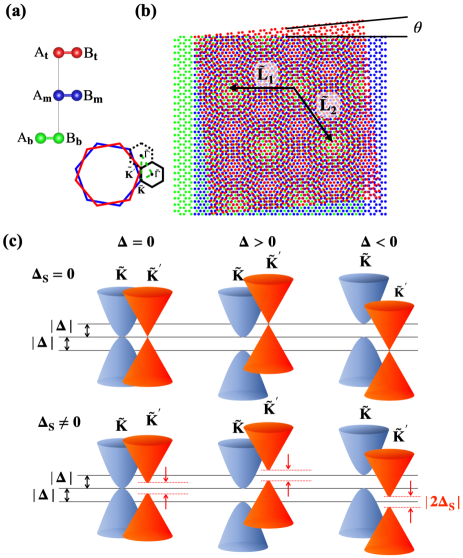
In this paper, we investigate the possibility of nearly flat bands in twisted monolayer graphene stacked on top of Bernal stacked bilayer graphene (tMBG), also known as twisted mono-bi graphene, where a linearly dispersing Dirac cone couples with a parabolic band. This is the next simplest system to build experimentally after twisted bilayer graphene where only one twist angle interface is present and can take advantage of the gate tunability of bilayer graphene where a gap can be opened by an external electric field. The possibility of nearly flat bands in tMBG had been hinted in earlier theoretical works Zhang et al. (2019a); Ma et al. (2019); Li et al. (2019b); Szendrő et al. (2020) and the first series of experiments in tMBG have been reported very recently Shi et al. (2020); Chen et al. (2020b); Polshyn et al. (2020). In this work we calculate various electronic structure properties relevant for interpreting experiments that had not been considered in earlier work, including a complete phase diagram in the parameter space of twist angle and interlayer potential difference for the valley Chern number, the ratio between the Coulomb interaction versus bandwidth, and the impact of a finite bandgap in the monolayer graphene that can appear when it is aligned with a hexagonal boron nitride substrate layer. This analysis is carried out using an improved full bands continuum Hamiltonian model that incorporates the remote hopping terms and the interlayer coupling matrix elements accounting for out of plane relaxation effects.
The manuscript is structured as follows. In Sec. II we define the model Hamiltonian of the system. The Sec. III is devoted to the discussion and presentation of various results in the parameter space of twist angle and interlayer potential difference proportional to for a number of observables of the system including the bandwidth , the ratio between the effective Coulomb interaction versus bandwidths , the (local) density of states, the valley Chern numbers of the low lying energy bands and associated Berry curvatures. In Sec. IV, we close the manuscript with the summary and conclusions.
II Model Hamiltonian
Our model Hamiltonian is based on the moire bands theory Bistritzer and MacDonald (2011); Jung et al. (2014) that expands beyond the proposal of Bistritzer-MacDonald of twisted bilayer graphene by incorporating information from first-principles calculations for both intralayer and interlayer moire patterns Jung et al. (2014). The description of our twisted monolayer-bilayer (tMBG) system is improved with respect to earlier works in Ref. Zhang et al. (2019a); Ma et al. (2019); Li et al. (2019b) by considering full bands continuum Hamitonian that incorporates renormalized out of plane tunneling parameters compatible with exact exchange and random phase approximation (EXX+RPA) equilibrium distances for different local stacking Chebrolu et al. (2019) and by incorporating the remote hopping parameters in the bilayer graphene Jung and MacDonald (2014). The Hamiltonian model of tMBG with a twist angle is given by
| (1) |
where the Hamiltonian elements for the bilayer graphene (BG) consisting of the bottom and middle layers have a a small onsite potential at the higher-energy dimer sites proportional to meV Jung and MacDonald (2014)
| (2) | ||||
where uses the graphene Hamiltonian with a rotated phase using graphene sublattice pseudospin Pauli matrices and and is a identity matrix. The rotation of the vector which is the momentum measured from valley introduces a phase proportional to . The valley index denote one of the two different Dirac points of the unrotated monolayer/bilayer graphene BZ. The result sin this work will be for the macro-valley unless stated otherwise. The Fermi velocity we used is defined through and relates to the intralayer nearest-neighbor hopping parameter value eV that is enhanced by 20% over the eV obtained within the local density approximation (LDA) Jung and MacDonald (2014) is a commonly used value in the graphene literature that is appropriate for band models that do not explicitly include non-local Coulomb interaction terms that can explicitly enhance the Fermi velocity. This enhanced value allows to capture the experimental moire bands features when the interlayer tunneling strengths are tuned to the first principles DFT calculation values for proper interlayer separation distances Chebrolu et al. (2019); Wong et al. (2015). The interlayer coupling terms within BG are given by
| (3) |
where contains the rotation dependent phase factor. The interlayer coupling matrix within the BG contains the perpendicular coupling term eV and the remote hopping contributions, including eV and eV adopted from the accurate tight-binding model of the bilayer graphene and cause trigonal warping and the electron-hole asymmetry Jung and MacDonald (2014). In the minimal model that we also present for comparison purposes, we ignore those remote hopping terms and the site-potential difference between the dimer and non-dimer sites in the BG Hamiltonian.
The interlayer coupling terms between the twisted G and BG systems are given by
| (4) |
where the three vectors are and with , and are
| (5) |
where , and . We chose the different values for and to consider the effect of out of plane atomic relaxation. Those parameters are adopted from EXX+RPA fitting values in the supplementary materials of Ref. Chebrolu et al. (2019). We use the interlayer potential values ( for the bottom, for top and for the middle layer) as
| (6) | ||||
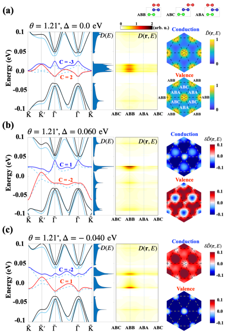
Following the schematic representation in Fig. 1, in loosely coupled sufficiently large twist angle tMBG it is possible to identify respectively simultaneous traces of quadratic bands from BG and linear bands from G near and of the moire Brillouin zone (MBZ). Their degree of hybridization changes with the interlayer coupling term and twist angle magnitude. The presence of contributes to opening the bandgap at the of the monolayer graphene and, although weakly, facilitates the isolation of the low energy nearly flat bands.
III Results and discussions
III.1 Flat bands
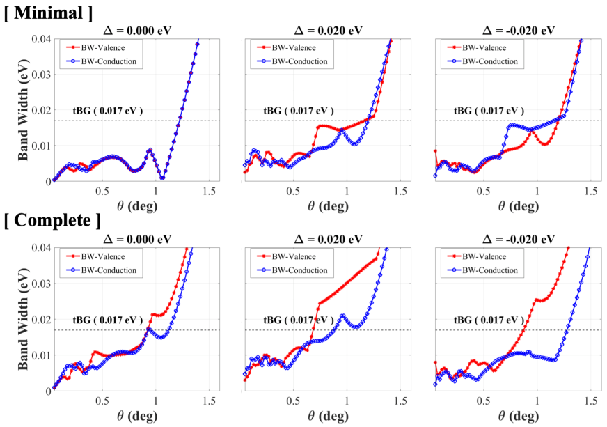
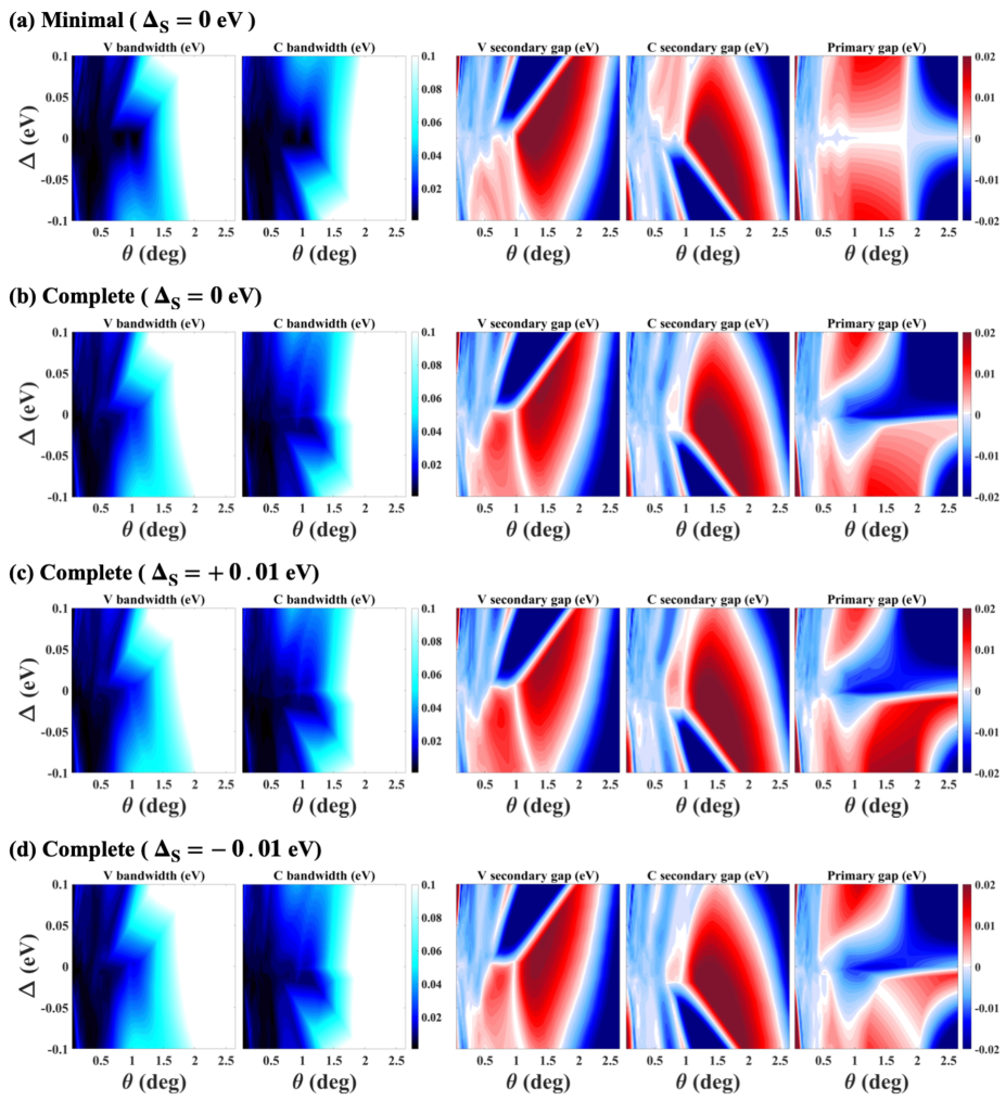
Here we explore the parameter space of twist angles and electric field induced interlayer potentials in search of the optimum conditions for the generation of isolated flat bands where we can expect to see correlation effects. Inspection of minimal model moire bands in tMBG shows that narrow bandwidths of the order of 1 meV are achievable near the magic angle comparable to the bandwidths seen for the flat bands in the minimal model tBG Chittari et al. (2018); Chebrolu et al. (2019), tDBG Chebrolu et al. (2019) and twisted multilayer graphene Liu et al. (2019b). When the remote hopping terms are added in the BG the bandwidths of the flat bands at the twist angle broaden up to 1520 meV. While the bandwidths see an increasing trend with twist angles, introducing interlayer potential differences of magnitudes meV often allows to reduce their bandwidths and allows to isolate them by opening a primary and secondary gaps, see appendix Fig. A1 and A2 for the relevant illustrations. Hence, even if the broadened bandwidths are less favorable than that of magic angle tBG due to the remote hopping terms, the presence of a finite interlayer potential difference allows to further tune the low energy bandwidths in tMBG in a manner similar to tDBG Chebrolu et al. (2019) or massive tBG Javvaji et al. (2020) when a bandgap opens at the primary Dirac point. While the conduction bandwidths tend to be narrower than those of the valence bands, we notice a strong electric field direction dependent asymmetry of the bandwidths when compared to tBG and tDBG that leads to minimum conduction bandwidths for and minimum valence bandwidths for . This trend can be verified to remain valid up to twist angles as large as beyond which the bandwidths increase steeply above 50 meV, see appendix Fig. A2.
The isolation of the flat bands due to the electric fields allows to characterize the valley resolved Chern number of the -th band through
| (7) |
where the Berry curvature is defined through D. et al. (2010)
| (8) |
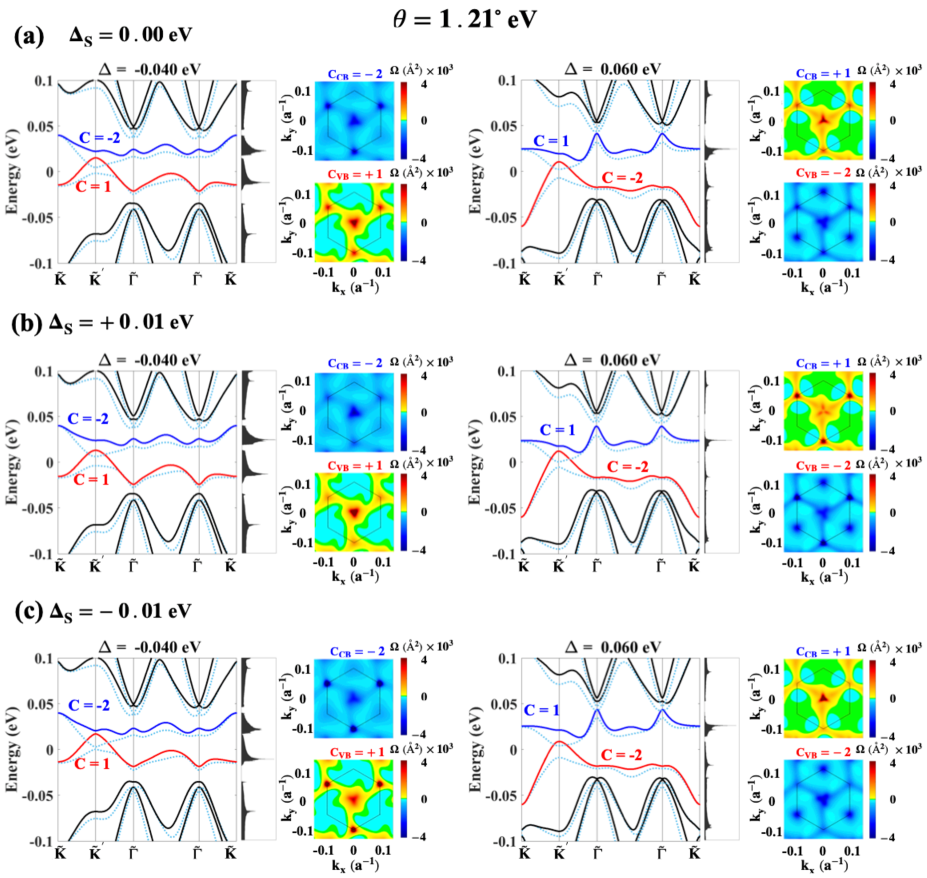
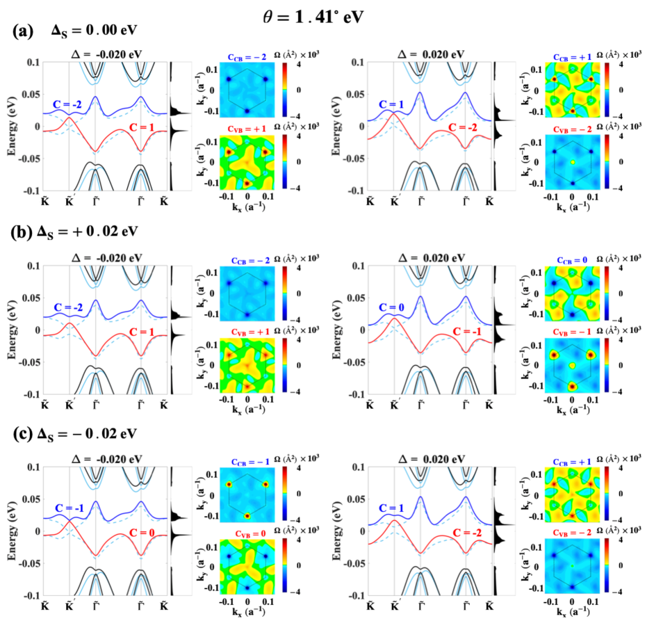
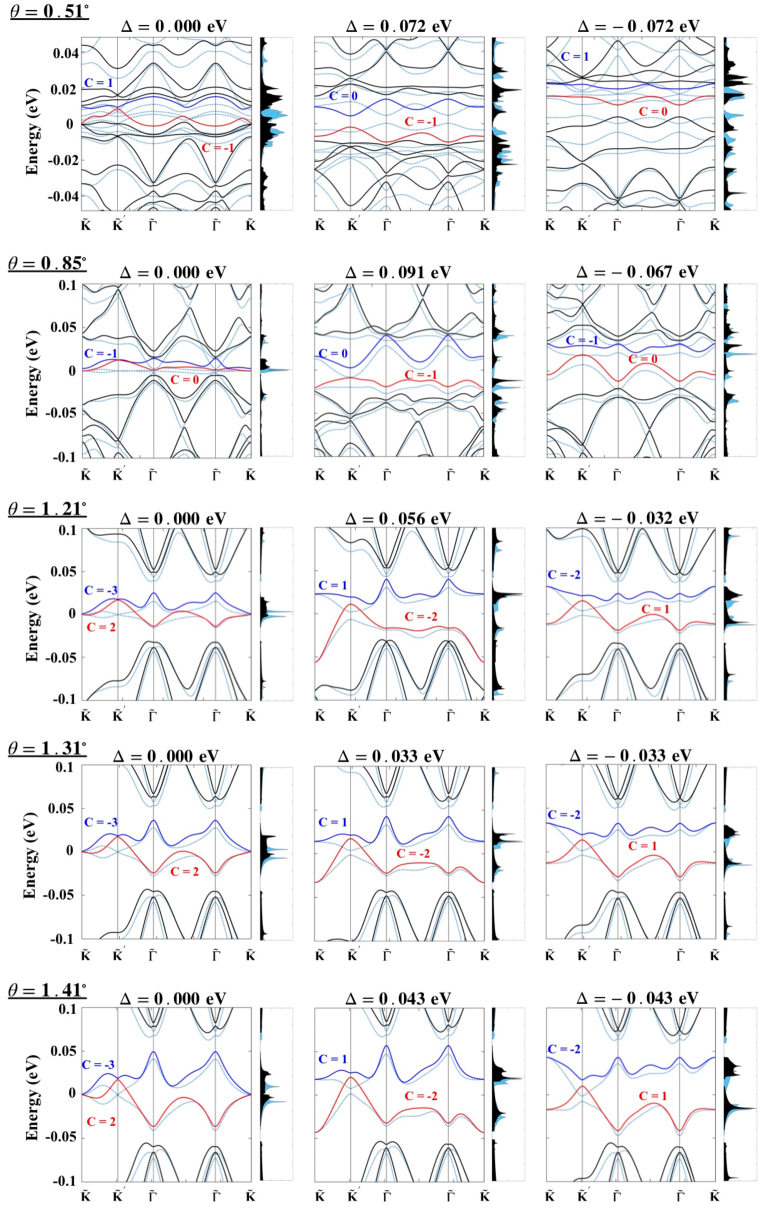
where is the moire Bloch states, and are the band energies. For instance, the low-energy valence band of tMBG at has a valley Chern number , and for the conduction band in the absence of an electric field (). Upon application of an electric field , we can trigger changes in the topological numbers both for conduction and valence bands. See Fig. 2 and the appendix Fig. A3 for a closer illustration of the nearly flat bands prone to strong correlations for select twist angles 0.51∘, 0.85∘, 1.21∘, 1.31∘, and 1.41∘. In Fig. 2, we illustrated the band structures at for three different electric fields eV where the bandwidth of valence or conduction bands reach minima values. Switching the direction of the interlayer potential differences allows to achieve different valley Chern numbers for the valence/conduction bands, respectively, and whose values can be reversed with the sign of the electric field.
Isolation of the low energy flat bands from the neighboring bands can be aided through and parameters that can open gaps in the bilayer and monolayer components of tMBG. As we mentioned earlier, when the monolayer and bilayer bands are loosely coupled for large twist angles, we can distinguish the linearly dispersing bands at of the monolayer graphene and the quadratic bands at for the bottom BG, see Eq. (6). While gaps in the bilayer component near can be opened with , it won’t open for the Dirac cone of monolayer graphene at which instead can be achieved by aligning an hBN layer Hunt et al. (2013); Amet et al. (2013); Jung et al. (2015). This effect can be captured through a site-potential difference representing an average constant staggered potential difference between the two sub-lattices and and can be used as an additional control parameter for tMBG. In the appendix Fig. A2 (c) and (d), we illustrate how the bandwidths, primary and secondary band gaps change for different signs of the sublattice staggered potentials or depending on the relative alignment of hBN contacting the monolayer graphene. We notice that a staggered potential generally improves the isolation of the bands even if the total bandwidths are similar to the case. The staggered potential due to hBN has also an effect on the topology of the low energy bands. In Fig. A4, we presented the band structures of tMBG at and with staggered potentials of eV for select values of electric fields. Here, we observe that the sign differences in introduces small changes in the band structure but leads to non-negligible changes in the local density of states and, at times, to the valley Chern numbers which in turn can impact the transport properties.
III.2 Local density of states
The local density of states (LDOS) maps in tMBG behave analogously to those of tBG in the fact that the charge densities tend to concentrate at local stacking configurations where the monolayer and top bottom layer units cells are on top of each other at the ABB stacking configurations, see Fig. 2 (a). The sensitivity of the flat bands to interlayer potential differences and sublattice staggering potential discussed earlier suggests that the electron localization properties can also be tuned by means of those system control knobs. For this purpose we define the normalized LDOS difference as for finite interlayer potential or staggered potential where the tildes indicate normalization and the energy is chosen to sit at the van Hove singularity of the flat band under consideration. The increase and decrease of LDOS happen mainly at the ABC and ABA stacking locations for variable as noted in Fig. 2. For that increases the population of the electrons at the bottom layer we observe an overall increase of valence band electrons at ABA and depletion at ABC, and general depletion at both ABA and ABC for the conduction band electrons. Reversing the electric field for favoring the accumulation of electrons at the top layer reverses this overall behavior but enhancing the population at both ABA and ABC stacking locations for the conduction bands and depleting for the valence bands. Significant changes in the LDOS maps are seen also when we introduce a finite as illustrated in Fig. A4 where the height of the LDOS at ABB stacking can change significantly depending also on the other system parameters. This observation is in keeping with the fact that the electron wave functions of the flat bands locate primarily at the low energy carbon sites of the bilayer and at the carbon sublattice of the monolayer right on top of the bilayer low energy site, see appendix Fig. A5.
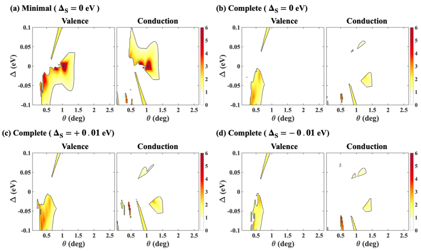
III.3 Strong correlations at large U/W regions
The diagram in Fig. 3 relating the Coulomb interaction strength against the bandwidth show that maxima spots are possible for twist angles for the valence flat bands and for the conduction bands under appropriate interlayer potentials , generally more favorable for when the electric fields favor accumulation of electrons in the top layer, although either field directions can generate isolated flat bands for the larger twist angles. Further introduction of the staggered potential on the monolayer of modifies the phase diagram generally enlarging and reducing its area respectively for positive and negative , in particular near and . In order to estimate the Coulomb interaction strength we adopted the formula for the effective three-dimensional screened Coulomb potential which can be written as
| (9) |
where we used and the Debye length which includes the 2D density of states . The moire length depends on graphene’s lattice constant and twist angle , is the moire supercell area, denotes the band widths, and is the heaviside step function such that enhances screening in the presence of band overlap for negative values of the primary and secondary gaps . From the formula in Eq. (9), we can identify the parameter space in and with large prone to strong correlations for both valence and conduction bands. In Fig. 3 we compare the results of between the minimal model and complete model, and consider the staggered potential ( eV) that can be introduced by alignment of the monolayer graphene with hBN. The phase diagram for has a strong electron-hole asymmetry and sign dependence to that is naturally expected from the structural asymmetry of tMBG and was not observed in tBG Chittari et al. (2018) and tDBG Chebrolu et al. (2019). We notice that even the symmetry of the diagram between the electron and hole flat bands for opposite signs present for the minimal model is destroyed when the remote hopping terms in the BG Hamiltonian introduce significant overlap between neighboring bands.
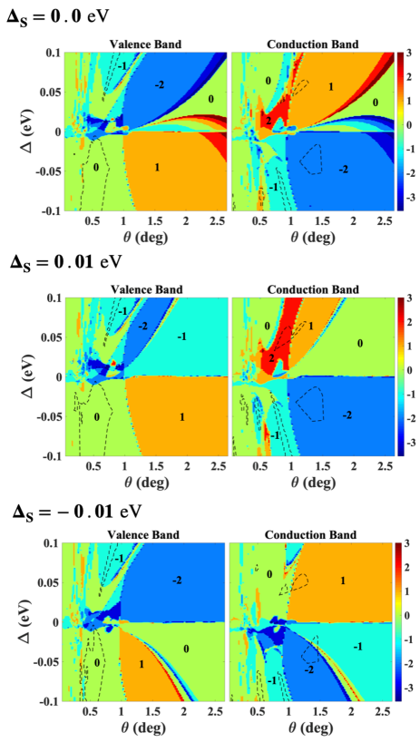
III.4 Topological moire bands
Well defined non-trivial valley Chern numbers are expected in isolated moire bands and they are believed to underlie the spontaneous quantum Hall effects observed in experiments when the degeneracy of the flat bands are lifted by Coulomb interactions Chen et al. (2020a); Sharpe et al. (2019); Serlin et al. (2019). The valley Chern numbers that we calculated following Eq. (7) range the values of for the low-energy valence and conduction bands in the parameter space of and as we show in the Fig. 4 and is further modified through as shown in appendix Figs. A6-A7. For the minimal model (not shown) a certain degree of symmetry is preserved in the Chern number phase diagram for the valence and conductions bands of opposite signs as we had noted for the phase diagram. With the remote hopping terms included the valley Chern numbers for the most promising flat bands take values of for the conduction bands in the vicinity of for and for . The Chern number is for the flat bands expected at for valence and conduction bands with opposite electric fields, and a Chern number of is expected for the valence flat bands near for . We observe contrasting behaviors for with the negative and positive valley Chern numbers of respectively for most valence and conduction bands, while for they assume values of . The strong electron-hole asymmetry together with the large tunability of the band structures with the electric fields makes of tMBG an intersting system where it is possible to access multiple valley Chern number regions.
IV Summary and conclusions
In this paper we investigated the conditions for the onset of strongly correlated topological flat bands in twisted monolayer graphene on Bernal stacked bilayer graphene (tMBG) as a function of twist angle and interlayer potential parameters. Proper inclusion of the remote hopping terms in the bilayer graphene enhances broadening of the low energy bandwidths and introduces overlap between neighboring bands reducing the parameter space of strongly correlations where the ratio between the effective Coulomb interactions and bandwidths remain large. However, a finite interlayer potential by a perpendicular electric field can reduce the bandwidth and isolate the low energy bands by opening primary and secondary band gaps. The system responds asymmetrically to the electric field direction for both valence and conduction bands resulting in multiple islands of large regions. We have summarized in Fig. 3 together with the valley Chern numbers in Fig. 4 the conditions for strong correlations in the valence or conduction bands that we expect for twist angles in the range of and for appropriate interlayer potential differences, more specifically in islands around twist angles of . The bandwidths are narrowest for small twist angles and they quickly increase above 50 meV for twist angles larger than precluding strong correlations for large twist angles despite that the bands can be isolated through a perpendicular electric field. This phase diagram can be further altered by an average sublattice staggering potential that can be introduced in the monolayer graphene through alignment with a hexagonal boron nitride layer. We have shown that the tunability of the bandwidths, band isolation, and valley Chern numbers through the twist angle and interlayer potential differences makes of tMBG a more versatile system than twisted bilayer graphene for generating nearly flat moire bands prone to strong correlations.
V Acknowledgments.
This work was supported by the Samsung Science and Technology Foundation under project No. SSTF-BA1802-06 for Y. P. and the Basic Science Research Program through the National Research Foundation of Korea (NRF) funded by the Ministry of Education Grants No. 2018R1A6A1A06024977 and Grant No. NRF-2020R1A2C3009142 for B.L.C., and by the Basic Study and Interdisciplinary R&D Foundation Fund of the University of Seoul (2019) for J.J.
References
- Hass et al. (2008) J. Hass, F. Varchon, J. E. Millán-Otoya, M. Sprinkle, N. Sharma, W. A. de Heer, C. Berger, P. N. First, L. Magaud, and E. H. Conrad, Phys. Rev. Lett. 100, 125504 (2008).
- Miller et al. (2009) D. L. Miller, K. D. Kubista, G. M. Rutter, M. Ruan, W. A. de Heer, P. N. First, and J. A. Stroscio, Science 324, 924 (2009).
- Miller et al. (2010) D. L. Miller, K. D. Kubista, G. M. Rutter, M. Ruan, W. A. de Heer, P. N. First, and J. A. Stroscio, Phys. Rev. B 81, 125427 (2010).
- Sadowski et al. (2006) M. L. Sadowski, G. Martinez, M. Potemski, C. Berger, and W. A. de Heer, Phys. Rev. Lett. 97, 266405 (2006).
- De Heer et al. (2010) W. A. De Heer, C. Berger, X. Wu, M. Sprinkle, Y. Hu, M. Ruan, J. A. Stroscio, P. N. First, R. Haddon, B. Piot, et al., J. Phys. D: Appl. Phys. 43, 374007 (2010).
- Brihuega et al. (2012) I. Brihuega, P. Mallet, H. González-Herrero, G. Trambly de Laissardière, M. M. Ugeda, L. Magaud, J. M. Gómez-Rodríguez, F. Ynduráin, and J.-Y. Veuillen, Phys. Rev. Lett. 109, 196802 (2012).
- Ohta et al. (2012) T. Ohta, J. T. Robinson, P. J. Feibelman, A. Bostwick, E. Rotenberg, and T. E. Beechem, Phys. Rev. Lett. 109, 186807 (2012).
- Lopes dos Santos et al. (2012) J. M. B. Lopes dos Santos, N. M. R. Peres, and A. H. Castro Neto, Phys. Rev. B 86, 155449 (2012).
- Lopes dos Santos et al. (2007) J. M. B. Lopes dos Santos, N. M. R. Peres, and A. H. Castro Neto, Phys. Rev. Lett. 99, 256802 (2007).
- Shallcross et al. (2010) S. Shallcross, S. Sharma, E. Kandelaki, and O. A. Pankratov, Phys. Rev. B 81, 165105 (2010).
- Shallcross et al. (2008) S. Shallcross, S. Sharma, and O. A. Pankratov, Phys. Rev. Lett. 101, 056803 (2008).
- Landgraf et al. (2013) W. Landgraf, S. Shallcross, K. Türschmann, D. Weckbecker, and O. Pankratov, Phys. Rev. B 87, 075433 (2013).
- Shallcross et al. (2013) S. Shallcross, S. Sharma, and O. Pankratov, Phys. Rev. B 87, 245403 (2013).
- Bistritzer and MacDonald (2011) R. Bistritzer and A. H. MacDonald, Proc. Natl. Acad. Sci. U.S.A. 108, 12233 (2011).
- Moon and Koshino (2013) P. Moon and M. Koshino, Phys. Rev. B 87, 205404 (2013).
- Moon and Koshino (2012) P. Moon and M. Koshino, Phys. Rev. B 85, 195458 (2012).
- Jung et al. (2014) J. Jung, A. Raoux, Z. Qiao, and A. MacDonald, Phys. Rev. B 89, 205414 (2014).
- San-Jose et al. (2012) P. San-Jose, J. González, and F. Guinea, Phys. Rev. Lett. 108, 216802 (2012).
- San-Jose and Prada (2013) P. San-Jose and E. Prada, Phys. Rev. B 88, 121408 (2013).
- Stauber et al. (2013) T. Stauber, P. San-Jose, and L. Brey, New J. Phys. 15, 113050 (2013).
- Bistritzer and MacDonald (2010) R. Bistritzer and A. H. MacDonald, Phys. Rev. B 81, 245412 (2010).
- Wang et al. (2012) Z. Wang, F. Liu, and M. Chou, Nano Lett. 12, 3833 (2012).
- Schmidt et al. (2014) H. Schmidt, J. C. Rode, D. Smirnov, and R. J. Haug, Nat Commun 5, 5742 (2014).
- Carr et al. (2018) S. Carr, S. Fang, P. Jarillo-Herrero, and E. Kaxiras, Phys. Rev. B 98, 085144 (2018).
- Koshino et al. (2018) M. Koshino, N. F. Q. Yuan, T. Koretsune, M. Ochi, K. Kuroki, and L. Fu, Phys. Rev. X 8, 031087 (2018).
- Kang and Vafek (2019) J. Kang and O. Vafek, Phys. Rev. Lett. 122, 246401 (2019).
- Tarnopolsky et al. (2019) G. Tarnopolsky, A. J. Kruchkov, and A. Vishwanath, Phys. Rev. Lett. 122, 106405 (2019).
- Po et al. (2019) H. C. Po, L. Zou, T. Senthil, and A. Vishwanath, Phys. Rev. B 99, 195455 (2019).
- Cao et al. (2018a) Y. Cao, V. Fatemi, A. Demir, S. Fang, S. L. Tomarken, J. Y. Luo, J. D. Sanchez-Yamagishi, K. Watanabe, T. Taniguchi, E. Kaxiras, et al., Nature 556, 80 (2018a).
- Kim et al. (2017) K. Kim, A. DaSilva, S. Huang, B. Fallahazad, S. Larentis, T. Taniguchi, K. Watanabe, B. J. LeRoy, A. H. MacDonald, and E. Tutuc, Proc. Natl. Acad. Sci. U.S.A. 114, 3364 (2017).
- Sharpe et al. (2019) A. L. Sharpe, E. J. Fox, A. W. Barnard, J. Finney, K. Watanabe, T. Taniguchi, M. A. Kastner, and D. Goldhaber-Gordon, Science 365, 605 (2019).
- Cao et al. (2018b) Y. Cao, V. Fatemi, S. Fang, K. Watanabe, T. Taniguchi, E. Kaxiras, and P. Jarillo-Herrero, Nature 556, 43 (2018b).
- Yankowitz et al. (2019) M. Yankowitz, S. Chen, H. Polshyn, Y. Zhang, K. Watanabe, T. Taniguchi, D. Graf, A. F. Young, and C. R. Dean, Science 363, 1059 (2019).
- Cao et al. (2020) Y. Cao, D. Chowdhury, D. Rodan-Legrain, O. Rubies-Bigorda, K. Watanabe, T. Taniguchi, T. Senthil, and P. Jarillo-Herrero, Phys. Rev. Lett. 124, 076801 (2020).
- Wong et al. (2015) D. Wong, Y. Wang, J. Jung, S. Pezzini, A. M. DaSilva, H.-Z. Tsai, H. S. Jung, R. Khajeh, Y. Kim, J. Lee, et al., Phys. Rev. B 92, 155409 (2015).
- Kerelsky et al. (2019) A. Kerelsky, L. J. McGilly, D. M. Kennes, L. Xian, M. Yankowitz, S. Chen, K. Watanabe, T. Taniguchi, J. Hone, C. Dean, et al., Nature 572, 95 (2019).
- Choi et al. (2019) Y. Choi, J. Kemmer, Y. Peng, A. Thomson, H. Arora, R. Polski, Y. Zhang, H. Ren, J. Alicea, G. Refael, et al., Nat. Phys. 15, 1174 (2019).
- Yankowitz et al. (2012) M. Yankowitz, J. Xue, D. Cormode, J. D. Sanchez-Yamagishi, K. Watanabe, T. Taniguchi, P. Jarillo-Herrero, P. Jacquod, and B. J. LeRoy, Nat. Phys 8, 382 (2012).
- Song et al. (2015) J. C. W. Song, P. Samutpraphoot, and L. S. Levitov, Proc. Natl. Acad. Sci. U.S.A. 112, 10879 (2015).
- Javvaji et al. (2020) S. Javvaji, J.-H. Sun, and J. Jung, Phys. Rev. B 101 (2020).
- Chen et al. (2019a) G. Chen, L. Jiang, S. Wu, B. Lyu, H. Li, B. L. Chittari, K. Watanabe, T. Taniguchi, Z. Shi, J. Jung, et al., Nat. Phys 15, 237 (2019a).
- Chen et al. (2019b) G. Chen, A. L. Sharpe, P. Gallagher, I. T. Rosen, E. J. Fox, L. Jiang, B. Lyu, H. Li, K. Watanabe, T. Taniguchi, et al., Nature 572, 215–219 (2019b).
- Chittari et al. (2019) B. L. Chittari, G. Chen, Y. Zhang, F. Wang, and J. Jung, Phys. Rev. Lett. 122, 016401 (2019).
- Zhang et al. (2019a) Y.-H. Zhang, D. Mao, Y. Cao, P. Jarillo-Herrero, and T. Senthil, Phys. Rev. B 99, 075127 (2019a).
- Chebrolu et al. (2019) N. R. Chebrolu, B. L. Chittari, and J. Jung, Phys. Rev. B 99, 235417 (2019).
- Liu et al. (2019a) X. Liu, Z. Hao, E. Khalaf, J. Y. Lee, K. Watanabe, T. Taniguchi, A. Vishwanath, and P. Kim, arXiv:1903.08130 (2019a).
- Lee et al. (2019) J. Y. Lee, E. Khalaf, S. Liu, X. Liu, Z. Hao, P. Kim, and A. Vishwanath, Nat Commun 10, 5333 (2019).
- Shen et al. (2020) C. Shen, Y. Chu, Q. Wu, N. Li, S. Wang, Y. Zhao, J. Tang, J. Liu, J. Tian, K. Watanabe, et al., Nat. Phys (2020).
- Choi and Choi (2019) Y. W. Choi and H. J. Choi, Phys. Rev. B 100, 201402 (2019).
- Koshino (2019) M. Koshino, Phys. Rev. B 99, 235406 (2019).
- Li et al. (2019a) X. Li, F. Wu, and S. D. Sarma, arXiv:1906.08224 (2019a).
- Chittari et al. (2018) B. L. Chittari, N. Leconte, S. Javvaji, and J. Jung, Electronic Structure 1, 015001 (2018).
- Zhang et al. (2019b) Y.-H. Zhang, D. Mao, and T. Senthil, Phys. Rev. Research 1, 033126 (2019b).
- Bultinck et al. (2020) N. Bultinck, S. Chatterjee, and M. P. Zaletel, Phys. Rev. Lett. 124, 033126 (2020).
- Haldane (1988) F. D. M. Haldane, Phys. Rev. Lett. 61, 2015 (1988).
- Kane and Mele (2005) C. L. Kane and E. J. Mele, Phys. Rev. Lett. 95, 146802 (2005).
- Nandkishore and Levitov (2010) R. Nandkishore and L. Levitov, Phys. Rev. B 82, 115124 (2010).
- Jung et al. (2011) J. Jung, F. Zhang, and A. H. MacDonald, Phys. Rev. B 83, 115408 (2011).
- Zhang et al. (2011) F. Zhang, J. Jung, G. A. Fiete, Q. Niu, and A. H. MacDonald, Phys. Rev. Lett. 106, 156801 (2011).
- Chen et al. (2020a) G. Chen, A. L. Sharpe, E. J. Fox, Y.-H. Zhang, S. Wang, L. Jiang, B. Lyu, H. Li, K. Watanabe, T. Taniguchi, et al., Nature 579, 56–61 (2020a).
- Serlin et al. (2019) M. Serlin, C. L. Tschirhart, H. Polshyn, Y. Zhang, J. Zhu, K. Watanabe, T. Taniguchi, L. Balents, and A. F. Young, Science 367, 900 (2019).
- Ma et al. (2019) Z. Ma, S. Li, Y.-W. Zheng, M.-M. Xiao, H. Jiang, J.-H. Gao, and X. C. Xie, arXiv:1905.00622 (2019).
- Li et al. (2019b) X. Li, F. Wu, and A. H. MacDonald (2019b), eprint 1907.12338.
- Szendrő et al. (2020) M. Szendrő, P. Süle, G. Dobrik, and L. Tapasztó, arXiv:2001.11462 (2020).
- Shi et al. (2020) Y. Shi, S. Xu, M. M. A. Ezzi, N. Balakrishnan, A. Garcia-Ruiz, B. Tsim, C. Mullan, J. Barrier, N. Xin, B. A. Piot, et al., arXiv:2004.12414 (2020).
- Chen et al. (2020b) S. Chen, M. He, Y.-H. Zhang, V. Hsieh, Z. Fei, K. Watanabe, T. Taniguchi, D. H. Cobden, X. Xu, C. R. Dean, et al., arXiv:2004.11340 (2020b).
- Polshyn et al. (2020) H. Polshyn, J. Zhu, M. A. Kumar, Y. Zhang, F. Yang, C. L. Tschirhart, M. Serlin, K. Watanabe, T. Taniguchi, A. H. MacDonald, et al., arXiv:2004.11353 (2020).
- Jung and MacDonald (2014) J. Jung and A. H. MacDonald, Phys. Rev. B 89, 035405 (2014).
- Liu et al. (2019b) J. Liu, Z. Ma, J. Gao, and X. Dai, Phys. Rev. X 9, 031021 (2019b).
- D. et al. (2010) X. D., C. M.-C., and N. Q., Rev. Mod. Phys. 82, 1959 (2010).
- Hunt et al. (2013) B. Hunt, J. D. Sanchez-Yamagishi, A. F. Young, M. Yankowitz, B. J. LeRoy, K. Watanabe, T. Taniguchi, P. Moon, M. Koshino, P. Jarillo-Herrero, et al., Science 340, 1427 (2013).
- Amet et al. (2013) F. Amet, J. R. Williams, K. Watanabe, T. Taniguchi, and D. Goldhaber-Gordon, Phys. Rev. Lett. 110, 216601 (2013).
- Jung et al. (2015) J. Jung, A. M. DaSilva, A. H. MacDonald, and S. Adam, Nat Commun 6, 6308 (2015).
Appendix
A1. Bandwidth as a function of twist angle
The bandwidth of the -th band at a given twist angle is calculated as . We show the bandwidth variation as a function of twist angle for tMBG in Fig A1. As it is observed in the twisted bilayer graphene (tGB), the bandwidth of the low energy bands decreases together with twist angle and reaches local minima at certain angles. In the minimal model of tMBG the bandwidth of the low-energy bands (valence/conduction) decreases with twist angle reaching the lowest bandwidth at . In contrast to the minimal model, the complete model that includes the remote hopping terms shows broadened bandwidths that have markedly different behaviors depending on the two signs (negative/positive) of , indicating the electric field direction dependent asymmetry on the bandwidth in tMBG.
A2. Bandwidth phase diagrams
Identification of isolated low energy bands is important in order to achieve strongly correlated phases. In the presence of a primary gap near charge neutrality given by , the isolation of the flat bands from higher energy bands can be identified through a secondary gap. For the valence band the secondary gap is and similarly for the conduction band it is . The positive value of indicates isolation and a negative value indicates overlap with the higher energy bands. It is understood from appendix A1 that the bandwidths of valence/conduction bands in tMBG are tunable with the electric field and depends on the sign of . In Fig. A2, we show the valence/conduction bands bandwidth, secondary, and primary gaps phase diagrams for the parameter space of twist angle () and electric field (). It is clear that (See Fig. A2 (a) and (b)), the bandwidth minima do not evolve linearly with twist angle () nor does with electric field () in both minimal and complete models. The primary gap vanished in the complete model for most of the positive electric fields . In the main text we introduced a staggered potential to open the gap of the monolayer graphene’s linear bands of tMBG which has also an effect in the band isolation and bandwidth minimum. In Fig. A2 (c) and (d) for the complete model, we show respectively the effects of positive and negative staggered potentials. In the presence of a staggered potential (), the parameter space for the primary gap is increased, as well as the secondary gaps in the conduction bands for positive electric fields.
A3. Promising twist angles and band structures
The electronic structure for promising flat band system parameters are shown in Fig. A3 for select twist angles (0.51∘, 0.85∘, 1.21∘, 1.31∘, and 1.41∘) for values that isolate either the conduction or the valence flat bands. The bandwidth and isolation of the low-energy bands of tMBG depend on the sign of electric field . The valley Chern number of the isolated bands are sensitive to the sign and magnitude of .
A4. Effect of staggered potential () on valley Chern numbers
The electric field is not sufficient to open the gap between the linear bands associated to the monolayer graphene in tMBG. In the main text, we defined a staggered potential () to introduce a gap at the monolayer linear bands that enhanced the isolation and further reduced the bandwidth of low the energy bands of tMBG. From appendix A3, it is known that the topology of the nontrivial bands can be modified with . Here we show that the staggered potential () can also impact the valley Chern numbers of the low energy bands for appropriate twist angle and interlayer potential by comparing the calculations of the electronic structure for specific twist angles 1.21∘ and 1.41∘ for different sets of and values shown in Figs. A6 A7.
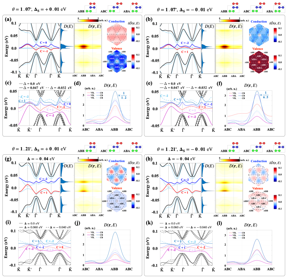
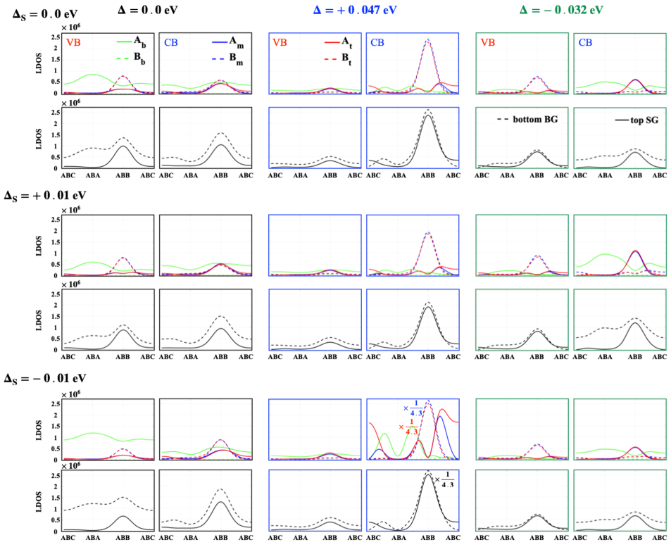
A5. Sub-lattice and twisted layer resolved local density of states at twist angle
The LDOS at the twist angle are mainly located at the ABB stacking in tMBG regardless of the value for . In Fig. A5, we further show by projecting the LDOS onto the sub-lattices that the charge localization at the ABB stacking concentrate mainly at the low energy Ab and Bm sites of the bilayer and the vertically contiguous Bt of the monolayer. The low energy sub-lattice Bm of the bilayer has the dominant contribution over all the low energy sub-lattices. In the presence of an applied electric field, the localization completely polarized to the sub-lattices Bt and Bm, and further inclusion of a staggered potential influences the localization where a negative increases the LDOS on sub-lattices Bt and Bm by almost an order of magnitude. We expect the preferential occupation of the low energy sites by the flat bands for other twist angles while changes introduced by may behave differently. This type of electron localization behaviors could in principle be observed through scanning probe measurements.