From Transparent Conduction to Coulomb Blockade at Fixed Hole Number
Abstract
We present a complex set of transport spectroscopy data on a clean single-wall carbon nanotube device in high magnetic fields. At zero axial field, the device displays in hole conduction with increasingly negative gate voltage a fast transition towards high contact transparency and eventually Fabry-Pérot interference of conductance. When increasing the axial field component up to , the contact transparency and the overall conductance are reduced all the way to Coulomb blockade, clearly displaying the subsequent charging with the first 10 holes. The continuous transition between the transport regimes is dominated by a rich spectrum of Kondo-like resonances, with distinct features in the stability diagrams.
I Introduction
Carbon nanotubes provide a prototypical, highly versatile system for quantum transport, which has been the topic of extensive research over the last decades Laird et al. (2015). They have allowed the observation of electronic transport regimes as different as Coulomb blockade Tans et al. (1997); Margańska et al. (2019), Kondo effect-dominated tunneling Nygård et al. (2000); Götz et al. (2018), and electronic Fabry-Pérot interference Liang et al. (2001); Dirnaichner et al. (2016). A striking property of suspended, so-called “ultraclean” nanotube devices Margańska et al. (2019); Cao et al. (2005) is that the effective transparency of contacts can be tuned over a large range by application of a gate voltage alone, while maintaining the regularity of the confinement potential. In combination with analysis of the repetitive shell filling, this has led to studies on the evolution of transport regimes with tunnel coupling Makarovski et al. (2007a); Anders et al. (2008); Yang et al. (2020).
When the absolute number of electrons or holes, as opposed to the shell filling, is relevant, investigating the dependence of the spectrum on barrier transparencies becomes more challenging. Approaches that have been pursued here include comparing hole and electron spectrum Niklas et al. (2016) (which utilizes electron-hole symmetry) or introducing additional barrier gates Benyamini et al. (2014) (which requires more complex fabrication).
Here, we present data on the transport spectrum in the few-hole regime, where the contacts are transparent and typically a transition to Fabry-Pérot interference of conductance is observed Liang et al. (2001); Dirnaichner et al. (2016). Application of an axial magnetic field of up to reduces the conductance in our device, leading via multiple Kondo-like transport resonances Nygård et al. (2000); Götz et al. (2018); Goldhaber-Gordon et al. (1998); Jarillo-Herrero et al. (2005a); Schmid et al. (2015a) all the way to strong Coulomb blockade, at a then known number of holes in the valence band. A comprehensive theoretical model for the data is so far still missing, however, we hope to inspire corresponding work. In order to facilitate this, the raw data of the measurements presented here is deposited online under an open access license Schmid et al. (2020).
II Device and measurement
The inset of Figure 1 displays a schematic of the measured device. Using chemical vapor deposition (CVD) Kong et al. (1998), a carbon nanotube has been grown in situ across predefined, 40 nm thick rhenium contacts and a trench between them; the highly doped silicon chip substrate is used as a global back gate. The contact distance, as approximation for the suspended length of the nanotube segment, is . During the CVD process, the contact metal surface is saturated with carbon Götz et al. (2016); barely any traces of superconductivity in the contacts can be found in the transport measurements.
The device was very stable, surviving multiple cool-downs in different cryostats with only minor changes, and very clean in the sense of highly regular transport spectra. Its characteristics in parameter ranges other than discussed here have already been presented in several publications Margańska et al. (2019); Götz et al. (2018); Schmid et al. (2012, 2015b); Stiller et al. (2020). The device shows the typical behaviour of a small-bandgap carbon nanotube. For positive gate voltages , i.e., in electron conductance, strong Coulomb blockade with a repetitive shell filling pattern can be observed (not shown); the tunnel barriers here are formed by a wide p-n junction within the carbon nanotube Margańska et al. (2019); Park and McEuen (2001); Kuemmeth et al. (2008). The electronic band gap is observed at a low positive gate voltage.
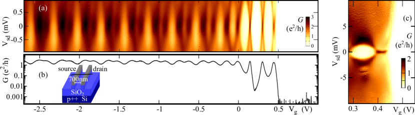
Figures 1(a–c) show pre-characterization measurements of hole transport, for , performed in the vacuum of a helium-3 cryostat at . The differential conductance as function of gate voltage and bias voltage is plotted in Fig. 1(a). While at this temperature close to the band gap edge Coulomb blockade related effects are still visible, the transition into electronic Fabry-Pérot interference with a strongly broadened, oscillatory pattern and a conductance always exceeding Yang et al. (2020) is clear for . This is also demonstrated by the zero bias conductance trace plotted in Fig. 1(b), which shows a behaviour strongly resembling, e.g., data published in Dirnaichner et al. (2016), including the onset of a Sagnac interference-induced modulation.
On closer observation, the precise nature of the conductance oscillations near the electronic band gap already turns out to be more complex than expected. Figure 1(c) shows a detail measurement of the rapid conductance onset at the gap edge. The measurement exhibits no indications of further structure within the gap region even at high bias, strong filtering and wide-range logarithmic color scale plotting, indicating that the nanotube is here fully depleted of free carriers. The first electron enters the conductance band at with a sharp Coulomb oscillation (not shown). Conversely, the low-bias conductance maximum near resolves into a structure broadly extended in , allowing for speculation that it represents a Kondo ridge with already the addition of two holes Nygård et al. (2000); Götz et al. (2018).
III Large axial magnetic field
In the following, all presented data has been recorded at base temperature of a top-loading dilution refrigerator, with the device immersed into the diluted phase of the liquid 3He/4He mixture. The dilution refrigerator was equipped with a superconducting magnet and a rotateable sample holder, such that the relative orientation of the magnetic field and the carbon nanotube could be adjusted within the chip surface plane.
Our central observation is shown in Fig. 2. It plots the zero-bias conductance in the few-hole regime, as function of both gate voltage and magnetic field in the direction of the carbon nanotube axis , over a wide field range .
At low magnetic field, left edge of the plot, the transition towards Fabry-Pérot interference Liang et al. (2001); Dirnaichner et al. (2016) with an overall increasing conductance is visible. For further clarity, the conductance trace of the data set has been overlaid as a white line plot; exceeds around . It shows several oscillations; comparing the gate voltage scale of the broad ridge in the region with the high field behaviour discussed below and with Fig. 1 indicates that we observe here already a -periodic phenomenon, at the transition between SU(4) Kondo effect and Fabry-Pérot interference Yang et al. (2020).
Conversely, at high axial magnetic field, up to at the right edge of the plot, the overall conductance is significantly lower, and the nanotube device displays well-separated Coulomb oscillations of conductance. A careful search at the edge of the band gap region has not shown any indications of further features in hole conductance at more positive . This allows to identify the absolute number of holes in the system in Coulomb blockade, see the numbers at the right edge of the plot.
The transition from transparent conductance to Coulomb blockade behaviour, filling the central area of the plot, displays an extraordinary degree of complexity. Kondo-like resonances cross Coulomb blockade areas, with different levels of background (cotunneling) conductance on either side of them. They merge into diagonal features in the plot, for lower field passing to more positive gate voltages. From a theory perspective, the transition has to involve a reduction of the charging energy per hole from being the dominant energy scale to nearly zero, giving an indication of the expected multitude of phenomena.
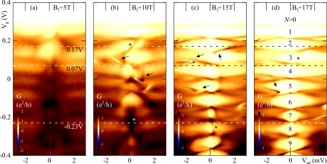
Extending the data of Fig. 2, Fig. 3 plots stability diagrams, i.e., the differential conductance as function of bias voltage and gate voltage , for fixed values of the magnetic field in each panel. At comparatively low magnetic field , only strongly broadened patterns can be observed, see Fig. 3(a). At , Fig. 3(b), first features resembling diamond-shaped Coulomb blockade regions emerge. They are strongly distorted and broadened, overlaid by a wide zero-bias ridge of enhanced conductance at , and by strongly bias-dependent resonances as, e.g., at . The trend towards lower conductance and more regular Columb blockade regions continues with , Fig. 3(c), where except for the region near the zero-bias conductance anomalies are nearly gone, and , Fig. 3(d).
IV Detail observations
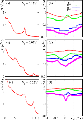
To gain insight into the nature of the “diagonally running resonances” in the magnetoconductance spectrum of Fig. 2, in Fig. 4 we plot selected line traces both from Fig. 2 and Fig. 3. We chose gate voltages such that at the magnetic fields of the stability diagrams of Fig. 3 such a resonance is observed. The corresponding gate voltages are marked in Fig. 2 and Fig. 3 with dashed lines.
For the first two panels, Fig. 4(a,b), the gate voltage is ; at this voltage, a resonance crosses , see the white cross in Fig. 2. This resonance becomes clearly visible again in the line cut of Fig. 4(a) as a distinct local maximum of conductance. Fig. 4(b) shows the corresponding bias traces of the panels of Fig. 3, at . The trace at immediately stands out with a (near) zero bias anomaly of conductance, suggesting a Kondo-like behaviour of the observed phenomenon. Surprisingly, the conductance maximum displays a strong gate voltage dependence in Fig. 3(b).
Similar behaviour of the line traces is observed in Fig. 4(c,d) at and in Fig. 4(e,f) at . For Fig. 4(c,d), and , the corresponding region in the stability diagram of Fig. 3(a) resembles a Coulomb blockade degeneracy point; it also evolves at higher magnetic field into the transition. In the case of Fig. 4(e,f) at and , the zero-bias conductance maximum corresponds to a wide region in Fig. 3(b) similar to merged Kondo ridges. In addition, in the latter panels, also the conductance feature near but not exactly at translates into a conductance maximum in bias dependence. Note that the data indicates a global shift of all features in bias on the order of , most likely due to an input offset of the current amplifier. On close observation the same offset is also visible in Fig. 3.
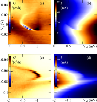
A surprising detail of the stability diagrams of Fig. 3 is the presence of several sickle-shaped features of positive, low, or even strong negative differential conductance, see the arrows in the figure. Two of the corresponding regions are enlarged in Fig. 5, each accompanied by the simultaneously measured dc current.
The precise origin of these features is unknown; their shape does not correspond to typical single electron tunneling or cotunnelling phenomena. Given that the measurement took place with the device immersed in liquid helium, and that a high magnetic field was present, mechanical self-activation is unlikely to be the cause Schmid et al. (2012, 2015b); Steele et al. (2009); Wen et al. (2020); Urgell et al. (2020). A self-driving mechanism would need to overcome both viscous damping and dissipation due to induction. An unambiguous decision whether the sharpest such features here in our measurement are sudden switching events, as expected for the onset of mechanical instability, is not possible from the data set due to the averaging times of lock-in amplifier and multimeter. Some of the sickle-shaped features in Fig. 3 are, however, clearly broadened, see, e.g., the region enlarged in Fig. 5(c,d), also speaking against a vibrational instability phenomenon.
V Further data
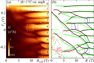
In Fig. 6(a), the magnetic field is kept constant at its maximum value, , but the sample holder is rotated stepwise; the magnetic field remains in the chip surface plane, but the relative orientation of nanotube axis and field changes. The plot shows the differential conductance as function of gate voltage and axial magnetic field component , with as the angle between field direction and nanotube axis. The overall similarity between Fig. 6(a) and Fig. 2 immediately confirms that the axial field component is crucial for the suppression of overall conductance and for most of the observed spectrum features. On closer observation, however, there are subtle deviations in the conductance resonance pattern between the figures, indicating that the large angle-independent Zeeman energy here modifies the transport spectrum. Three particularly clear cases where resonance lines visible in Fig. 2 are absent in Fig. 6(a) are marked with dashed rectangles in the figure.
Figure 6(b) explicitly compares the two measurements. Local maxima have been extracted from traces and plotted as points; based on these points, lines have been drawn manually to connect them, also taking account step-like features in the data that did not trigger the maximum search. As last step, the two sets of points and lines have been superimposed. Red points and black lines stem from the data of Fig. 2, where an axial magnetic field of varied strength is applied; green points and green lines stem from Fig. 6(a), where at fixed magnetic field value the angle between nanotube and field and with that the axial component is varied. As expected, at the right edge of the plot, with (or ) the patterns coincide. For smaller field or larger angle, the deviations gradually increase; the three resonances missing in Fig. 6(a) are marked again with dashed lines.
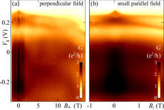
Figure 7(a) plots the conductance in the case of a magnetic field perpendicular to the nanotube axis, . The overall signal remains large, and only broad features occur. Around zero magnetic field, a gate voltage independent pattern of larger conductance is visible, which may be related to superconductivity in the rhenium contacts.
Finally, Fig. 7(b) shows a detail measurement at low parallel magnetic field . Again, around zero field, larger conductance is observed, consistent with an impact of the contact metal independent of the precise in-plane orientation of the magnetic field.
VI Discussion
While significant research has been published regarding carbon nanotubes grown in-situ over metal contacts, the precise interface properties and contact geometries in low-temperature experiments still pose open questions. In the case of electron transport, quantum dot confinement is typically given by an electrostatically induced p-n junction within the nanotube, and the contacts to the quantum dot are formed by segments of the nanotube itself beyond these junctions. The nanotube-metal interface can be treated as small perturbation or even neglected Margańska et al. (2019); Park and McEuen (2001). This is, however, not the case for hole transport (i.e., negative applied gate voltages), where the p-n junction is absent.
Regarding the overall suppression of conductance with increasing axial magnetic field, it has been demonstrated recently that cross-quantization affects in such a field the shape of electronic wave functions along the carbon nanotube axis Margańska et al. (2019); Stiller et al. (2020). This leads to smaller tunnel rates to the contacts in the high field limit. The observation in Margańska et al. (2019) and the corresponding theoretical analysis was, however, targeted at the case of single electron states in a well-closed off system. It may require extension or modification for transparent contacts and interacting charges.
In Grove-Rasmussen et al. (2012), also an impact of a magnetic field on the tunnel coupling is discussed, though state-specific for KK’-mixed doublet states and on a smaller magnetic field scale. The mechanism proposed in Grove-Rasmussen et al. (2012) is that the axial field modifies the circumferential wave function and with that the wavefunction overlap at a side contact. Given that in our device the nanotube lies on top of the contacts, this may well be relevant specifically in the hole regime.
Regarding carbon nanotube transport spectra in magnetic fields, many works have demonstrated complex results including multiple ground state transitions as well as, e.g., Kondo phenomena caused by nontrivial degeneracies Jarillo-Herrero et al. (2005a); Schmid et al. (2015a); Grove-Rasmussen et al. (2012); Jarillo-Herrero et al. (2005b); Deshpande and Bockrath (2008). The gradual transition between transport regimes has been studied mostly via the impact of a changing gate voltage on a repetitive shell filling pattern in linear response Makarovski et al. (2007a); Anders et al. (2008); Yang et al. (2020); Babić and Schönenberger (2004); Makarovski et al. (2007b). This has allowed to observe and model the emergence of the Kondo effect in its SU(2) and SU(4) manifestation and the transition between Coulomb blockade and Fabry-Pérot oscillations Anders et al. (2008); Yang et al. (2020). The interplay of Kondo transport, where on-site repulsion (i.e., charging energy) is still relevant, and quantum interference in an open system however still poses conceptual challenges, recently leading to the proposal of “correlated Fabry-Pérot oscillations” in the transition regime Yang et al. (2020).
Finally, features quite similar to the diagonal lines of Fig. 2 can be found in Grove-Rasmussen et al. (2012), see Fig. 3(c) there. The authors describe their observations as cotunneling corresponding to magnetic-field induced level crossings; a functional renormalization group calculation is used to successfully model many details of their measurements. Similar approaches may be able to cover at least part of the parameter range of our data shown in Fig. 2.
VII Conclusions
We present millikelvin transport spectroscopy measurements on a well-characterized carbon nanotube device Margańska et al. (2019); Götz et al. (2018); Schmid et al. (2012, 2015b), where in a strong axial magnetic field the entire range of transport regimes from transparent conduction to Coulomb blockade can be traced at well-known absolute hole number. A multitude of quantum ground state transitions and Kondo-like resonances emerges in the interacting few-hole system. While similar phenomena have been observed and analyzed for smaller parameter spaces in literature, see, e.g., Grove-Rasmussen et al. (2012), a theoretical description covering strong Coulomb blockade, the Kondo regime, as well as quantum interference in an open conductor in a consistent way is still lacking. Our raw data is available to the interested reader Schmid et al. (2020); we hope to inspire corresponding work.
Acknowledgements.
The authors acknowledge funding by the Deutsche Forschungsgemeinschaft via Emmy Noether grant Hu 1808/1, SFB 631, SFB 689, and SFB 1277, and by the Studienstiftung des Deutschen Volkes. A. K. H. acknowledges support from the Visiting Professor program of the Aalto University School of Science. We would like to thank M. Grifoni, M. Margańska, and P. Hakonen for insightful discussions, and Ch. Strunk and D. Weiss for the use of experimental facilities. The data has been recorded using Lab::Measurement Reinhardt et al. (2019).References
- Laird et al. (2015) E. A. Laird, F. Kuemmeth, G. A. Steele, K. Grove-Rasmussen, J. Nygård, K. Flensberg, and L. P. Kouwenhoven, “Quantum transport in carbon nanotubes,” Rev. Mod. Phys. 87, 703–764 (2015).
- Tans et al. (1997) Sander J. Tans, Michel H. Devoret, Hongjie Dai, Andreas Thess, Richard E. Smalley, L. J. Geerligs, and Cees Dekker, “Individual single-wall carbon nanotubes as quantum wires,” Nature 386, 474 (1997).
- Margańska et al. (2019) M. Margańska, D. R. Schmid, A. Dirnaichner, P. L. Stiller, Ch. Strunk, M. Grifoni, and A. K. Hüttel, “Shaping electron wave functions in a carbon nanotube with a parallel magnetic field,” Phys. Rev. Lett. 122, 086802 (2019).
- Nygård et al. (2000) J. Nygård, H. C. Cobden, and P. E. Lindelof, “Kondo physics in carbon nanotubes,” Nature 408, 342 (2000).
- Götz et al. (2018) K. J. G. Götz, D. R. Schmid, F. J. Schupp, P. L. Stiller, Ch. Strunk, and A. K. Hüttel, “Nanomechanical characterization of the Kondo charge dynamics in a carbon nanotube,” Phys. Rev. Lett. 120, 246802 (2018).
- Liang et al. (2001) W. Liang, M. Bockrath, D. Bozovic, J. H. Hafner, M. Tinkham, and H. Park, “Fabry-Pérot interference in a nanotube electron waveguide,” Nature 411, 665 (2001).
- Dirnaichner et al. (2016) A. Dirnaichner, M. del Valle, K. J. G. Götz, F. J. Schupp, N. Paradiso, M. Grifoni, Ch. Strunk, and A. K. Hüttel, “Secondary electron interference from trigonal warping in clean carbon nanotubes,” Phys. Rev. Lett. 117, 166804 (2016).
- Cao et al. (2005) J. Cao, Q. Wang, and H. Dai, “Electron transport in very clean, as-grown suspended carbon nanotubes,” Nature Materials 4, 745–749 (2005).
- Makarovski et al. (2007a) A. Makarovski, J. Liu, and G. Finkelstein, “Evolution of transport regimes in carbon nanotube quantum dots,” Phys. Rev. Lett. 99, 066801 (2007a).
- Anders et al. (2008) Frithjof B. Anders, David E. Logan, Martin R. Galpin, and Gleb Finkelstein, “Zero-bias conductance in carbon nanotube quantum dots,” Phys. Rev. Lett. 100, 086809 (2008).
- Yang et al. (2020) W. Yang, C. Urgell, S. L. De Bonis, M. Marganska, M. Grifoni, and A. Bachtold, “Fabry-Pérot oscillations in correlated carbon nanotubes,” (2020), arXiv:2003.08226.
- Niklas et al. (2016) M. Niklas, S. Smirnov, D. Mantelli, M. Marganska, N.-V. Nguyen, W. Wernsdorfer, J.-P. Cleuziou, and M. Grifoni, “Blocking transport resonances via Kondo many-body entanglement in quantum dots,” Nat. Commun. 7, 12442 (2016).
- Benyamini et al. (2014) A. Benyamini, A. Hamo, S. Viola Kusminskiy, F. von Oppen, and S. Ilani, “Real-space tailoring of the electron-phonon coupling in ultraclean nanotube mechanical resonators,” Nature Physics 10, 151–156 (2014).
- Goldhaber-Gordon et al. (1998) D. Goldhaber-Gordon, Hadas Shtrikman, D. Mahalu, David Abusch-Magder, U. Meirav, and M. A. Kastner, “Kondo effect in a single-electron transistor,” Nature 391, 156 (1998).
- Jarillo-Herrero et al. (2005a) P. Jarillo-Herrero, J. Kong, H. S. J. van der Zant, C. Dekker, L. P. Kouwenhoven, and S. De Franceschi, “Orbital Kondo effect in carbon nanotubes,” Nature 434, 484 (2005a).
- Schmid et al. (2015a) D. R. Schmid, S. Smirnov, M. Margańska, A. Dirnaichner, P. L. Stiller, M. Grifoni, A. K. Hüttel, and Ch. Strunk, “Broken SU(4) symmetry in a Kondo-correlated carbon nanotube,” Phys. Rev. B 91, 155435 (2015a).
- Schmid et al. (2020) D. R. Schmid, P. L. Stiller, A. Dirnaichner, and A. K. Hüttel, “Raw data for “From Transparent Conduction to Coulomb Blockade at Fixed Hole Number”,” (2020), zenodo; doi:10.5281/zenodo.4037354.
- Kong et al. (1998) J. Kong, H. T. Soh, A. M. Cassell, C. F. Quate, and H. Dai, “Synthesis of individual single-walled carbon nanotubes on patterned silicon wafers,” Nature 395, 878 (1998).
- Götz et al. (2016) K. J. G. Götz, S. Blien, P. L. Stiller, O. Vavra, T. Mayer, T. Huber, T. N. G. Meier, M. Kronseder, Ch. Strunk, and A. K. Hüttel, “Co-sputtered MoRe thin films for carbon nanotube growth-compatible superconducting coplanar resonators,” Nanotechnology 27, 135202 (2016).
- Schmid et al. (2012) D. R. Schmid, P. L. Stiller, Ch. Strunk, and A. K. Hüttel, “Magnetic damping of a carbon nanotube nano-electromechanical resonator,” New Journal of Physics 14, 083024 (2012).
- Schmid et al. (2015b) D. R. Schmid, P. L. Stiller, Ch. Strunk, and A. K. Hüttel, “Liquid-induced damping of mechanical feedback effects in single electron tunneling through a suspended carbon nanotube,” Appl. Phys. Lett. 107, 123110 (2015b).
- Stiller et al. (2020) P. L. Stiller, A. Dirnaichner, D. R. Schmid, and A. K. Hüttel, “Magnetic field control of the franck-condon coupling of few-electron quantum states,” Phys. Rev. B 102, 115408 (2020).
- Park and McEuen (2001) J. Park and P. L. McEuen, “Formation of a p-type quantum dot at the end of an n-type carbon nanotube,” Applied Physics Letters 79, 1363 (2001).
- Kuemmeth et al. (2008) F. Kuemmeth, S. Ilani, D. C. Ralph, and P. L. McEuen, “Coupling of spin and orbital motion of electrons in carbon nanotubes,” Nature 452, 448 (2008).
- Steele et al. (2009) G. A. Steele, A. K. Hüttel, B. Witkamp, M. Poot, H. B. Meerwaldt, L. P. Kouwenhoven, and H. S. J. van der Zant, “Strong coupling between single-electron tunneling and nanomechanical motion,” Science 325, 1103–1107 (2009).
- Wen et al. (2020) Yutian Wen, N. Ares, F. J. Schupp, T. Pei, G. A. D. Briggs, and E. A. Laird, “A coherent nanomechanical oscillator driven by single-electron tunnelling,” Nature Physics 16, 75–82 (2020).
- Urgell et al. (2020) C. Urgell, W. Yang, S. L. De Bonis, C. Samanta, M. J. Esplandiu, Q. Dong, Y. Jin, and A. Bachtold, “Cooling and self-oscillation in a nanotube electromechanical resonator,” Nature Physics 16, 32–37 (2020).
- Grove-Rasmussen et al. (2012) K. Grove-Rasmussen, S. Grap, J. Paaske, K. Flensberg, S. Andergassen, V. Meden, H. I. Jørgensen, K. Muraki, and T. Fujisawa, “Magnetic-field dependence of tunnel couplings in carbon nanotube quantum dots,” Phys. Rev. Lett. 108, 176802 (2012).
- Jarillo-Herrero et al. (2005b) P. Jarillo-Herrero, J. Kong, H. S. J. van der Zant, C. Dekker, L. P. Kouwenhoven, and S. De Franceschi, “Electronic transport spectroscopy of carbon nanotubes in a magnetic field,” Phys. Rev. Lett. 94, 156802 (2005b).
- Deshpande and Bockrath (2008) Vikram V. Deshpande and Marc Bockrath, “The one-dimensional Wigner crystal in carbon nanotubes,” Nature Physics 4, 314–318 (2008).
- Babić and Schönenberger (2004) B. Babić and C. Schönenberger, “Observation of Fano resonances in single-wall carbon nanotubes,” Phys. Rev. B 70, 195408 (2004).
- Makarovski et al. (2007b) A. Makarovski, A. Zhukov, J. Liu, and G. Finkelstein, “SU(2) and SU(4) Kondo effects in carbon nanotube quantum dots,” Phys. Rev. B 75, 241407 (2007b).
- Reinhardt et al. (2019) S. Reinhardt, C. Butschkow, S. Geissler, A. Dirnaichner, F. Olbrich, C. Lane, D. Schröer, and A. K. Hüttel, “Lab::Measurement — a portable and extensible framework for controlling lab equipment and conducting measurements,” Computer Physics Communications 234, 216–222 (2019).