Charge State Dynamics and Optically Detected Electron Spin Resonance Contrast of Shallow Nitrogen-Vacancy Centers in Diamond
Abstract
Nitrogen-vacancy (NV) centers in diamond can be used for nanoscale sensing with atomic resolution and sensitivity; however, it has been observed that their properties degrade as they approach the diamond surface. Here we report that in addition to degraded spin coherence, NV centers within nanometers of the surface can also exhibit decreased fluorescence contrast for optically detected electron spin resonance (OD-ESR). We demonstrate that this decreased OD-ESR contrast arises from charge state dynamics of the NV center, and that it is strongly surface-dependent, indicating that surface engineering will be critical for nanoscale sensing applications based on color centers in diamond.
Nitrogen-vacancy (NV) centers in diamond are actively explored for a number of applications in quantum information processing and sensing because they exhibit long spin coherence times at room temperature, and their spin states can be optically initialized and read out with off-resonant excitation Hong et al. (2013); Sage et al. (2013); Maurer et al. (2012); Hensen et al. (2015); Humphreys et al. (2018); Lovchinsky et al. (2016). In order to achieve strong interactions with materials and molecules that are external to the diamond, NV centers must be placed close to the diamond surface. It has been well established that the diamond surface can host contaminants, magnetic defects, and electronic defects that give rise to noise, leading to short spin coherence times Sangtawesin et al. (2019); Myers et al. (2014); De Oliveira et al. (2017); Grotz et al. (2011); Ohno et al. (2012); Naydenov et al. (2010); Ofori-Okai et al. (2012); Kim et al. (2015); Rosskopf et al. (2014); Romach et al. (2015), and recent work has shown that careful preparation of the diamond surface can mitigate this noise, leading to extended spin coherence times Sangtawesin et al. (2019); De Oliveira et al. (2017); Lovchinsky et al. (2016). Most NV center applications are based on the negative charge state of NV centers, NV-, and it is also known that NV centers can exist in the neutral charge state, NV0. It has been recently shown that both the steady-state charge populations under illumination and the equilibrium charge state in the dark of shallow NV centers can vary significantly from bulk properties Bluvstein et al. (2019); Stacey et al. (2019); Dhomkar et al. (2018); Yamano et al. (2017). Previous work has shown that charge state initialization can influence spin readout Hopper et al. (2020), however a detailed understanding of how these charge state dynamics can affect schemes for nanoscale sensing and its dependence on sample surface has not yet been established.
Here we demonstrate that the diamond surface can strongly affect both the steady-state charge state distribution and the charge state dynamics of NV centers within nanometers of the diamond surface, and that these charge state properties can significantly degrade optically detected electron spin resonance (OD-ESR) contrast. We focus on two diamond samples (samples A and F) that contain shallow NV centers introduced by ion implantation, which exhibit distinctly different OD-ESR contrast and charge state behavior. We find that sample A exhibits higher contrast, greater charge state stability in the dark, lower NV0 population under green illumination, and slower ionization and recombination dynamics than sample F. More specifically, we find that sample F exhibits charge state conversion rates that are comparable to the internal spin-dependent dynamics of the NV center, thus leading to decreased OD-ESR contrast. Finally, we measure time-resolved, spin-dependent photoluminescence (PL) and compare to a coupled rate equation model that incorporates charge conversion rates to quantitatively understand the impact of charge dynamics on OD-ESR contrast.
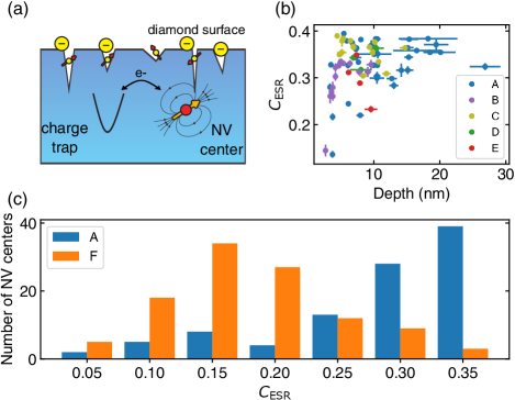
A cartoon schematic of the interactions between shallow NV centers and charge traps is depicted in Fig. 1(a). The surface can host defects that act as charge traps, and tunneling from NV centers to these charge traps gives rise to charge state instability, leading to a decrease in OD-ESR contrast of shallow NV centers Bluvstein et al. (2019).
Following Ref. Hopper et al. (2018), we define OD-ESR contrast as
| (1) |
where is the average number of photons collected in the readout pulse when the NV- spin state is initialized to the state. Figure 1(b) shows plotted for many NV centers as a function of depth across five samples, where depth is measured by detecting the proton NMR signal arising from the microscope immersion oil Pham et al. (2016). NV centers within of the surface display a wider distribution in .
In order to investigate the origin of the lower OD-ESR contrast, we identify two samples that have undergone nominally similar surface processing (see Supplemental Material Sec. I SI ), but exhibit markedly different distributions in , samples A and F [Fig. 1(c)]. Most NV centers in sample F exhibit below 0.3, as well as short coherence times (), precluding many NV characterization measurements, such as single-shot charge state readout Aslam et al. (2013) and using proton NMR to measure depth. We use this comparison to quantify the impact of charge state conversion on .
Both samples were prepared using nitrogen ion implantation followed by thermal annealing. Sample A was implanted with a nitrogen ion energy of while sample F was implanted with an energy of . Despite undergoing nominally similar surface processing, sample F contains persistent boron contamination comprising approximately 4 of a surface monolayer as measured by X-ray photoelectron spectroscopy SI , likely arising from contamination in the furnace during vacuum thermal annealing. We note that although sample F is expected to have a shallower distribution of NV centers because of its lower implantation energy, the distribution of is much lower than another sample that was prepared with the same ion implantation energy that does not exhibit surface contamination, sample B SI .
To understand the origin of the lower OD-ESR contrast in sample F, we examine the steady-state charge distributions in both samples. First we measure the PL spectrum under green illumination. We observe a significantly higher fraction of emission between the zero phonon line (ZPL) of NV0 (575 nm) and the ZPL of NV- (637 nm) in sample F, as well as a peak at 575 nm [Fig. 2(a)], indicating a higher steady-state population of NV0 Alsid et al. (2019). This higher NV0 steady-state population contributes to background fluorescence, decreasing the OD-ESR contrast proportionally.
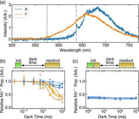
Recent work has shown that shallow NV centers can exhibit spontaneous conversion to NV0 without illumination Bluvstein et al. (2019). Here, we perform a similar measurement on several NV centers in both samples. First, the NV center charge state is initialized using a green pulse of sufficient length ( at ) to achieve a steady-state distribution. Then, after a variable time interval in the dark, we measure PL during an orange () pulse, which preferentially excites NV-, allowing for charge state readout. Normalizing to the PL at the shortest dark time interval, we observe that NV centers in sample F exhibit a decay in the NV- population over timescales between and to less than half of the initial value, while a decay of less than 25 is observed in sample A for dark times up to 1 second [Fig. 2(b)]. In sample A, we also perform the inverse measurement by initializing NV centers into NV0 using an orange pulse ( at , after a green pulse as Fig. 2(b) for consistency Dhomkar et al. (2018)) to look for evidence of spontaneous conversion to NV-. We observe no change in the NV- population out to 1 second [Fig. 2(c)], indicating that spontaneous charge conversion is very slow in this sample, regardless of the initial charge state population. This is consistent with previous hypotheses that spontaneous charge conversion is mediated by the availability of nearby electron traps at or near the surface [Fig. 1(a)] that strongly modify charge state kinetics Bluvstein et al. (2019).
Now we turn to the charge state conversion dynamics under illumination for both samples. The rate of change of the charge populations can be expressed in the following simplified model Aslam et al. (2013):
| (2) |
where is the NV- population, is the NV0 population, and and are ionization and recombination rates, respectively. Since the total population is conserved (), we can express the time dependence of the population in terms of a total charge conversion rate, , where .
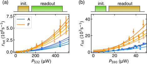
We measure charge conversion rates under green illumination by using a fixed orange pulse to initialize the NV centers primarily into NV0. Then under green illumination, the population shifts to NV-, and we fit the time-resolved PL to an exponential to extract . Similarly, we measure conversion rates under orange illumination by first initializing with a green pulse and measuring the overall ionization under orange, extracting in the same manner. Both data sets are plotted in Fig. 3 for a set of NV centers in samples A and F. We observe a clear quadratic power dependence for NV centers in both samples, consistent with both ionization and recombination being two-photon processes Aslam et al. (2013) (see Supplemental Material Sec. VI SI for a simplified derivation). NV centers in sample F have higher charge conversion rates under both green and orange illumination. Importantly, when the green power is comparable to the typical NV saturation power in our setup (), the charge state conversion rate can be faster than , comparable to the spin polarization rate for NV-, suggesting that fast ionization and recombination processes can occur during the spin initialization and readout times. Since these processes are not spin conserving Roberts et al. (2019), this fast charge conversion can lead to degradation of the OD-ESR contrast.
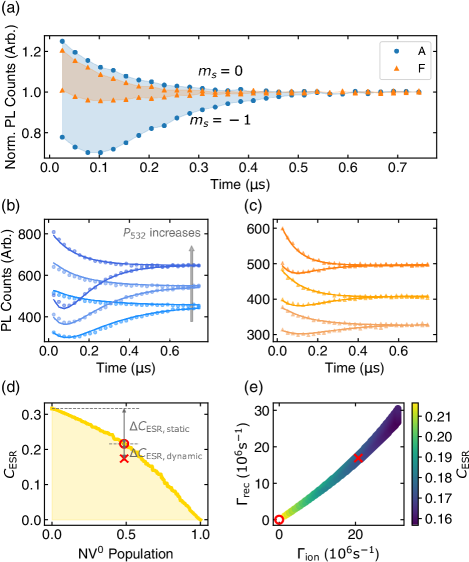
To quantify how charge state conversion rates affect OD-ESR contrast for NV centers under distinctly different surface environments, we measure the time-resolved PL during the green readout pulse. Example PL traces with initial NV- spin states (upper traces) and (lower traces) for NV centers in both samples are shown in Fig. 4(a). The area between the two sets of curves is proportional to , and in a typical sensing experiment, the readout conditions would be optimized to maximize this area. We observe that the total area between the curves for sample A is 3.6 times the area between the curves for sample F. We fit the data using a rate equation model for NV- spin dynamics Hacquebard and Childress (2018); Robledo et al. (2011); Roberts et al. (2019); Manson et al. (2006), modifying the model to additionally incorporate NV0 states and charge state conversion rates and (see a complete description of the rate equation model in Supplemental Material Sec. III SI ). In order to constrain the model, we measure PL traces for both and initial states for eight different laser powers and fit all data sets simultaneously to a single model. We constrain the fit to incorporate the same intrinsic NV parameters (excited state lifetime, singlet state lifetime, etc.) across all powers, while allowing the photo-induced transition rates to be free parameters. Representative PL traces for a subset of these powers for an NV center from sample A are shown in Fig. 4(b), and corresponding datasets from sample F are shown in Fig. 4(c). Our fitted intrinsic NV parameters are consistent with previously reported measurements Robledo et al. (2011); Roberts et al. (2019). We also find that extracted excited state and singlet lifetimes are consistent across NV centers. A summary of the extracted parameters for four NV centers in each sample can be found in Supplemental Material Sec. IV SI .
From the data it is clear that there are two different contributions of charge state dynamics to decreased : the increased background due to the steady-state NV0 population, and charge conversion rates interfering with spin dynamics. Armed with a model that quantitatively accounts for both spin and charge dynamics of the NV center, we use this model to disentangle the relative contributions to of these two effects. Using the fitted NV parameters, we vary and to simulate values of and the NV0 population. Using the extracted parameters for the NV center in sample F shown in Fig. 4(c), we plot the maximum as a function of steady-state NV0 population [Fig. 4(d)]. As expected, decreases monotonically as the NV0 population increases, and we define to be the decrease in due to the finite NV0 population.
Separately, as the overall and increase in magnitude, the charge conversion dynamics begin to compete with the spin dynamics, leading to an additional decrease in . We define this additional decrease at a given NV0 population as . We plot a contour of the simulated as a function of the charge state conversion rates at a fixed NV0 population [Fig. 4(e)], and we also observe a monotonic decrease of with increasing and .
For this particular NV center in sample F, where , we would expect an improvement to in the absence of any charge conversion, where and . By comparison, for the NV center from sample A shown in Fig. 4(b) with , the absence of charge conversion would yield a much smaller improvement in to 0.453, and .
We have shown that samples with different surface conditions can exhibit drastically different charge state dynamics for shallow NV centers, and that charge state stability can influence OD-ESR contrast in two ways: first, a high steady-state population in NV0 will increase the PL background and second, when the charge state conversion time is comparable to the NV spin polarization and readout time, ionization results in a loss of spin information and initialization, and consequently a decrease of . These effects can be drastically different for different diamond samples, as well as among NV centers in a given sample. These results point to the importance of surface preparation and engineering in utilizing NV centers for nanoscale sensing and magnetometry. On-going and future work includes establishing microscopic mechanisms for charge state instabilities, such as surface trap states and contaminants, as well as exploring optimal surface terminations Kaviani et al. (2014); Hauf et al. (2011); Stacey et al. (2015); Cui and Hu (2013) for stabilizing the negative charge state of shallow NV centers.
We thank James J. Allred for help with sample processing, Trisha Madhavan for help with part of the data acquisition, Haimei Zhang for help implementing the charge state readout optical setup, and Nan Yao, Yao-Wen Yeh, and John Schreiber at the Princeton Imaging and Analysis Center for help with diamond surface characterization. We also thank Dolev Bluvstein, Bo Dwyer, and Shimon Kolkowitz for helpful discussions. This material is based upon work supported by the U.S. Department of Energy, Office of Science, Office of Basic Energy Sciences, under Award Number DE-SC0018978. This work was also supported by the NSF under the CAREER program (Grant No. DMR-1752047), and was partially supported by the DARPA DRINQS program (Agreement No. D18AC00015). M. F. was supported by an appointment to the Intelligence Community Postdoctoral Research Fellowship Program by Oak Ridge Institute for Science and Education (ORISE) through an interagency agreement between the U.S. Department of Energy and the Office of the Director of National Intelligence (ODNI). L. V. H. R. acknowledges support from the Department of Defense through the National Defense Science and Engineering Graduate Fellowship Program.
References
- Hong et al. (2013) S. Hong, M. S. Grinolds, L. M. Pham, D. Le Sage, L. Luan, R. L. Walsworth, and A. Yacoby, MRS Bulletin 38, 155 (2013).
- Sage et al. (2013) D. L. Sage, K. Arai, D. R. Glenn, S. J. Devience, L. M. Pham, M. D. Lukin, A. Yacoby, A. Komeili, and R. L. Walsworth, Nature 496, 486 (2013).
- Maurer et al. (2012) P. C. Maurer, G. Kucsko, C. Latta, L. Jiang, N. Y. Yao, S. D. Bennett, F. Pastawski, D. Hunger, N. Chisholm, M. Markham, D. J. Twitchen, J. I. Cirac, and M. D. Lukin, Science 336, 1283 (2012).
- Hensen et al. (2015) B. Hensen, H. Bernien, A. E. Dreaú, A. Reiserer, N. Kalb, M. S. Blok, J. Ruitenberg, R. F. L. Vermeulen, R. N. Schouten, C. Abellán, W. Amaya, V. Pruneri, M. W. Mitchell, M. Markham, D. J. Twitchen, D. Elkouss, S. Wehner, T. H. Taminiau, and R. Hanson, Nature 526, 682 (2015).
- Humphreys et al. (2018) P. C. Humphreys, N. Kalb, J. P. J. Morits, R. N. Schouten, R. F. L. Vermeulen, D. J. Twitchen, M. Markham, and R. Hanson, Nature 558, 268 (2018).
- Lovchinsky et al. (2016) I. Lovchinsky, A. O. Sushkov, E. Urbach, N. P. De Leon, S. Choi, K. De Greve, R. Evans, R. Gertner, E. Bersin, C. Muller, L. McGuinness, F. Jelezko, R. L. Walsworth, H. Park, and M. D. Lukin, Science 351, 836 (2016).
- Sangtawesin et al. (2019) S. Sangtawesin, B. L. Dwyer, S. Srinivasan, J. J. Allred, L. V. Rodgers, K. De Greve, A. Stacey, N. Dontschuk, K. M. O’Donnell, D. Hu, D. A. Evans, C. Jaye, D. A. Fischer, M. L. Markham, D. J. Twitchen, H. Park, M. D. Lukin, and N. P. De Leon, Physical Review X 9, 031052 (2019).
- Myers et al. (2014) B. A. Myers, A. Das, M. C. Dartiailh, K. Ohno, D. D. Awschalom, and A. C. Bleszynski Jayich, Physical Review Letters 113, 027602 (2014).
- De Oliveira et al. (2017) F. F. De Oliveira, D. Antonov, Y. Wang, P. Neumann, S. A. Momenzadeh, T. Häußermann, A. Pasquarelli, A. Denisenko, and J. Wrachtrup, Nature Communications 8, 15409 (2017).
- Grotz et al. (2011) B. Grotz, J. Beck, P. Neumann, B. Naydenov, R. Reuter, F. Reinhard, F. Jelezko, J. Wrachtrup, D. Schweinfurth, B. Sarkar, and P. Hemmer, New Journal of Physics 13, 055004 (2011).
- Ohno et al. (2012) K. Ohno, F. Joseph Heremans, L. C. Bassett, B. A. Myers, D. M. Toyli, A. C. Bleszynski Jayich, C. J. Palmstrøm, and D. D. Awschalom, Applied Physics Letters 101, 082413 (2012).
- Naydenov et al. (2010) B. Naydenov, F. Reinhard, A. Lämmle, V. Richter, R. Kalish, U. F. D’Haenens-Johansson, M. Newton, F. Jelezko, and J. Wrachtrup, Applied Physics Letters 97, 242511 (2010).
- Ofori-Okai et al. (2012) B. K. Ofori-Okai, S. Pezzagna, K. Chang, M. Loretz, R. Schirhagl, Y. Tao, B. A. Moores, K. Groot-Berning, J. Meijer, and C. L. Degen, Physical Review B 86, 081406(R) (2012).
- Kim et al. (2015) M. Kim, H. J. Mamin, M. H. Sherwood, K. Ohno, D. D. Awschalom, and D. Rugar, Physical Review Letters 115, 087602 (2015).
- Rosskopf et al. (2014) T. Rosskopf, A. Dussaux, K. Ohashi, M. Loretz, R. Schirhagl, H. Watanabe, S. Shikata, K. M. Itoh, and C. L. Degen, Physical Review Letters 112, 147602 (2014).
- Romach et al. (2015) Y. Romach, C. Müller, T. Unden, L. J. Rogers, T. Isoda, K. M. Itoh, M. Markham, A. Stacey, J. Meijer, S. Pezzagna, B. Naydenov, L. P. McGuinness, N. Bar-Gill, and F. Jelezko, Physical Review Letters 114, 017601 (2015).
- Bluvstein et al. (2019) D. Bluvstein, Z. Zhang, and A. C. Jayich, Physical Review Letters 122, 76101 (2019).
- Stacey et al. (2019) A. Stacey, N. Dontschuk, J.-P. Chou, D. A. Broadway, A. K. Schenk, M. J. Sear, J.-P. Tetienne, A. Hoffman, S. Prawer, C. I. Pakes, A. Tadich, N. P. de Leon, A. Gali, and L. C. L. Hollenberg, Advanced Materials Interfaces 6, 1801449 (2019).
- Dhomkar et al. (2018) S. Dhomkar, H. Jayakumar, P. R. Zangara, and C. A. Meriles, Nano Letters 18, 4046 (2018).
- Yamano et al. (2017) H. Yamano, S. Kawai, K. Kato, T. Kageura, M. Inaba, T. Okada, I. Higashimata, M. Haruyama, T. Tanii, K. Yamada, et al., Japanese Journal of Applied Physics 56, 04CK08 (2017).
- Hopper et al. (2020) D. A. Hopper, J. D. Lauigan, T.-Y. Huang, and L. C. Bassett, Phys. Rev. Applied 13, 024016 (2020).
- Hopper et al. (2018) D. A. Hopper, H. J. Shulevitz, and L. C. Bassett, Micromachines 9, 437 (2018).
- Pham et al. (2016) L. M. Pham, S. J. Devience, F. Casola, I. Lovchinsky, A. O. Sushkov, E. Bersin, J. Lee, E. Urbach, P. Cappellaro, H. Park, A. Yacoby, M. Lukin, and R. L. Walsworth, Physical Review B 93, 045425 (2016).
- (24) “See Supplemental Material at http://link.aps.org/supplemental/ for details of samples, experimental procedures, rate equation model, and curve fitting.” .
- Aslam et al. (2013) N. Aslam, G. Waldherr, P. Neumann, F. Jelezko, and J. Wrachtrup, New Journal of Physics 15, 013064 (2013).
- Alsid et al. (2019) S. T. Alsid, J. F. Barry, L. M. Pham, J. M. Schloss, M. F. O’Keeffe, P. Cappellaro, and D. A. Braje, Physical Review Applied 12, 044003 (2019).
- Roberts et al. (2019) R. P. Roberts, M. L. Juan, and G. Molina-Terriza, Physical Review B 99, 174307 (2019).
- Hacquebard and Childress (2018) L. Hacquebard and L. Childress, Physical Review A 97, 063408 (2018).
- Robledo et al. (2011) L. Robledo, H. Bernien, T. V. D. Sar, and R. Hanson, New Journal of Physics 13, 025013 (2011).
- Manson et al. (2006) N. B. Manson, J. P. Harrison, and M. J. Sellars, Physical Review B 74, 104303 (2006).
- Kaviani et al. (2014) M. Kaviani, P. Deák, B. Aradi, T. Frauenheim, J. P. Chou, and A. Gali, Nano Letters 14, 4772 (2014).
- Hauf et al. (2011) M. V. Hauf, B. Grotz, B. Naydenov, M. Dankerl, S. Pezzagna, J. Meijer, F. Jelezko, J. Wrachtrup, M. Stutzmann, F. Reinhard, and J. A. Garrido, Physical Review B 83, 081304(R) (2011).
- Stacey et al. (2015) A. Stacey, K. M. O’Donnell, J.-P. Chou, A. Schenk, A. Tadich, N. Dontschuk, J. Cervenka, C. Pakes, A. Gali, A. Hoffman, and S. Prawer, Advanced Materials Interfaces 2, 1500079 (2015).
- Cui and Hu (2013) S. Cui and E. L. Hu, Applied Physics Letters 103, 051603 (2013).