Electron transparency of a Micromegas mesh
Abstract
Measurements of the electron transparency of a Micromegas mesh are compared to simulations. The flux conservation argument is shown to lead to inaccurate estimates of the transparency, the importance of accurate geometric modelling of the mesh is discussed and the effect of the dipole moment of the mesh is demonstrated. This study provides a validation of the microscopic simulation methods specifically developed for micropattern devices where the characteristic dimensions are of the same order of magnitude as the electron mean free path in the gas.
keywords:
Detector modelling and simulations II (electric fields, charge transport, multiplication and induction, pulse formation, electron emission, etc); Micropattern gaseous detectors (MSGC, GEM, THGEM, RETHGEM,MHSP,MICROPIC,MICROMEGAS, InGrid, etc); Charge transport and multiplication in gas1 Introduction
In Micromegas detectors [1, 2], a micro-mesh separates the drift region from the amplification region. We report on a detailed study, both experimental and theoretical, of the electron transparency of the mesh. The transparency enters in the gain calibration of the detector and is particularly important for a new generation of multi-gap detectors which are less prone to discharges [3].
2 Experimental set-up
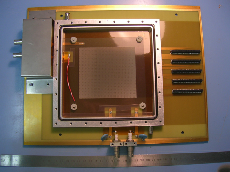
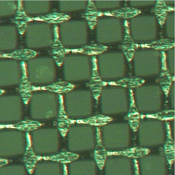
We have measured the transparency of a bulk-Micromegas [7] produced by CERN/EN-ICE, equipped with a calendered woven micro-mesh similar to the Micromegas detector of the TPC of the T2K experiment [8], see figure 1. The stainless-steel wires had a diameter of , a pitch of and the thickness of the mesh at the intersections of the wires was [9]. The amplification gap thickness was and the drift distance . The chamber was flushed with .
We have used an source, taking data at a rate of . The amplification field was which gave a gas gain of . The electric field in the drift region ranged from to . Signal amplitudes were calculated from the position of the photo peak, which has a resolution of . We estimate the mesh transparency as the ratio of the signal amplitude at a given drift field over the mean signal amplitude for . The typical uncertainty of the transparency is . The drift and amplification field are defined in this paper as the ratio of voltage difference over distance, respectively between cathode and mesh and between mesh and anode.
The anode of the detector was segmented in strips of width. The output of the 76 strips nearest to the source was summed and passed through a charge sensitive pre-amplifier acting as an integrator. Its decay time constant was , three orders of magnitude larger than the signal duration. Subsequently, it was fed to a unipolar semi-Gauss shaping amplifier (ORTEC model 571) with an integration time of . Finally, the measurements where digitised and recorded through a National Instruments PC-interface card.
3 Simulation
Since no exact solution is known for the field around a mesh, we have approximated the field using the finite element method and using the boundary element method. Despite the similarity in name, these techniques have strikingly different properties. The finite element method meshes the volume and parametrises the potential locally by means of quadratic polynomials. This potential is not as a rule a solution of the Maxwell equations and the resulting fields can be discontinuous across element boundaries, but the potential boundary conditions are strictly respected. The boundary element method meshes the surfaces of the electrodes and dielectrics. The fields are Maxwell-compliant and continuous, but the voltage boundary conditions are not necessarily strictly respected.
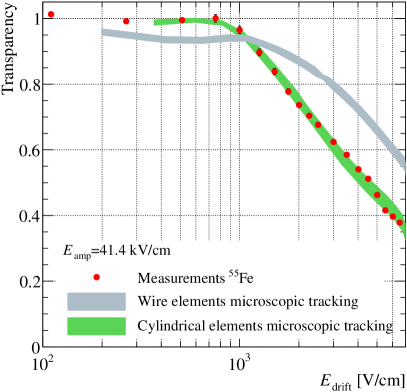
For the finite element approach, we have used the second-order tetrahedral elements with parabolic faces of Ansys [10]. These elements are well suited for curved structures such as mesh wires. Numerically, they are efficient since the iterative calculation of the isoparametric coordinates converges rapidly while the Jacobian of the final iteration serves to compute the potential gradient. The boundary element calculations were performed using neBEM [11, 12] which offers two elements with which a mesh can be modelled: one-dimensional thin-wire segments and three-dimensional polygonal approximations of cylinders. Wire elements are computationally attractive but the field is calculated using the thin-wire approximation. As a result, the voltage at one wire radius from the axis will only on average equal the imposed surface potential. When cylindric elements are used, the voltage boundary condition is applied to each of the surface panels of the cylinder.
Conservation of the flux of the electric field combined with the assumption that the electric flux is proportional with the electron flow, leads to a mesh transparency of where is the electric flux from the cathode to the anode and the flux from the cathode to the mesh. The flux ratio is easily calculated by means of Runge-Kutta-Fehlberg integration of the drift velocity vector.
The flux argument assumes that electrons actually follow the electric field, and thus neglects diffusion. To assess the impact of diffusion we have also calculated the transparency using microscopic electron tracking [5, 6]. This technique tries to reproduce electron transport at the molecular level. Electrons follow a vacuum trajectory between collisions. At each collision, one of the processes available in Magboltz [4] is selected at random, weighed by the probabilities for the various processes to occur, considering the electron energy prior to impact. An electron can lose energy in inelastic collisions, it may be lost to attachment, excite an atom or cause ionisation. Penning transfer, which has a comparatively minor impact in mixtures [13], was not taken into account.
For both integration techniques, the transparency was calculated by drifting electrons from randomly distributed points in the drift region, from the mesh. At this distance, the flux is uniform within the numerical precision and diffusion ensures that the transparency is decorrelated from the starting point. The transparency is estimated as the fraction of electrons arriving in the amplification region.
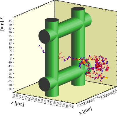
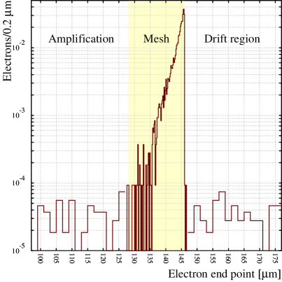
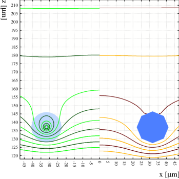
We do not present results for the more time consuming microscopic avalanche technique because it yielded essentially the same results as microscopic electron tracking in a few test cases. This is not surprising given that electron losses are concentrated on the drift side of the mesh while the electrons start multiplying only after they have passed the mesh, as seen in figure 2.
4 Results
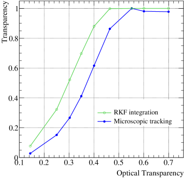
The measurements and the simulations are compared in figure 5. The measured transparency is constant for , beyond which electrons increasingly often hit the mesh. The transparency decreases to reach 40 % at . The microscopic transparency calculation agrees to 5 % with the measurements over the entire drift field range. This is true both for finite element and for boundary element field calculations. In contrast, the zero-diffusion transparency decreases only from and the transparency is overestimated by 20 % at . The difference between microscopic tracking and flux estimates is also clearly visible when predicting the electron transparency as a function of the wire pitch, see figure 4.
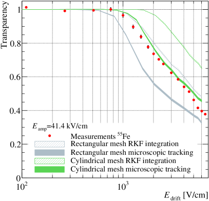
The sensitivity of the transparency to details of the geometry can be demonstrated by comparing two shapes of the mesh wires: a) rectangular mesh wires with sides equal to the actual mesh wire diameter, a simplification that is frequently made in such calculations; and b) realistic cylindric mesh wires (figure 2). In both cases, we assume that the mesh wires pass through one-another at the intersections – the mesh thickness at the wire intersections is in reality larger than the wire diameter. A rectangular wire mesh has the same optical transparency as a cylindric wire mesh, but it has a lower electron transparency because of the larger volume and larger surface area of the wires. The microscopic transparency for rectangular wires starts to decrease already at and the transparency is 20 % lower than the measurements at . The zero-diffusion calculation for rectangular wires happens to be in fair agreement with the measurements. These calculations have been performed using the finite element technique, but could equally well have been done with the boundary element method.
Simulations also reveal the importance of the dipole moment of the grid. In normal operation, the mesh as a whole is negatively charged – it repels electrons. To ensure an equal potential on both surfaces, there is additional positive charge on the drift side and an equal amount of negative charge on the amplification side. This leads to a dipole moment, as illustrated in figure 4. The thin-wire approximation neglects this dipole moment and leads to incorrect estimates of the transparency.
5 Conclusions
We have measured the electron transparency of a Micromegas mesh for a range of drift fields and have been able to reproduce these measurements with a microscopic calculation based on Magboltz, both using finite element and using boundary element field calculations. Zero-diffusion calculations, akin to the flux argument, fail to reproduce the measurements. Neither do calculations which oversimplify the geometry or neglect the dipole moment of the mesh.
Acknowledgements.
The R&D effort of the Muon ATLAS Micromegas Activity has been an important source of inspiration for this work. The measurements were performed in the RD51 collaboration laboratory at CERN during summer 2009. The hospitality of the RD51 collaboration which granted access to the common facilities is greatly appreciated. Fruitful discussions with Dimitris Fassouliotis and Christine Kourkoumelis are acknowledged. Supratik Mukhopadhyay and Nayana Majumdar, authors of neBEM, contributed to the calculations presented in this paper. This work was supported in part by the U.S. Department of Energy under contract No. DE-AC02-98CHI-886. K.N. acknowledges support from the Greek State Scholarships Foundation (I.K.Y.).References
- [1] G. Barouch et al., Development of a fast gaseous detector: Micromegas, Nucl. Instr. and Meth. A 423 (1999) 32–48.
- [2] Y. Giomataris et al., MICROMEGAS: a high-granularity position-sensitive gaseous detector for high particle-flux environments, Nucl. Instr. and Meth. A 376 (1996) 29–35.
- [3] Fabien Jeanneau et al., Double-mesh structure for ion back-flow suppression. Third RD51 collaboration meeting, Kolympari, Greece, 2009.
- [4] S.F. Biagi, Monte Carlo simulation of electron drift and diffusion in counting gases under the influence of electric and magnetic fields, Nucl. Instr. and Meth. A 421 (1999) 234–240.
- [5] H. Schindler et al., Calculation of gas gain fluctuations in uniform fields, Nucl. Instr. and Meth. A 624 (2010) 78–84.
- [6] R Veenhof, Numerical methods in the simulation of gas-based detectors, J. Instr. 4 (2009) P12017.
- [7] I. Giomataris et al., Micromegas in a bulk, Nucl. Instr. and Meth. A 560 (2006) 405–408.
- [8] Claudio Giganti and the T2K/ND280/TPC Collaboration, The test beams of the T2K TPC, J. Phys. Conf. Series 179 (2009) 012002.
- [9] R. de Oliveira. Private communication, 2010.
- [10] Ansys Inc., Ansys version 11 Electromagnetics, 2010.
- [11] N. Majumdar and S. Mukhopadhyay, Simulation of three-dimensional electrostatic field configuration in wire chambers: A novel approach, Nucl. Instr. and Meth. A 566 (2006) 489–494.
- [12] S. Mukhopadhyay et al., Electrostatics of micromesh based detectors, J. Instr. 4 (2009) P11004.
- [13] Ö. Şahin et al., Penning transfer in argon-based gas mixtures, J. Instr. 5 (2010) P05002.