TMDC Resonators for Second Harmonic Signal Enhancement
Abstract
In addition to their strong nonlinear optical response, transition metal dichalcogenides (TMDCs) possess a high refractive index in the visible and infrared regime. Therefore, by patterning those TMDCs into dielectric nanoresonators, one can generate highly confined electromagnetic modes. Controlled fabrication of TMDC nanoresonators does not only enhance the material’s intrinsic nonlinear response, but also allows for spatially shaping the emission via nanoresonator arrays. Here we fabricate patterned WS2 disks that support a high internal resonant electric field and show strong enhancement of second harmonic (SH) generation in the visible regime. In addition, we assemble the WS2 disks in arrays to spatially direct the coherent SH emission, in analogy to phased array antennas. Finally, we investigate and discuss drastic differences in the areal emission origin and intensity of the measured SH signals, which we find to depend on material variations of the used bulk WS2.
In their few-layer form, transition metal dichalcogenides (TMDCs) exhibit high nonlinear optical responses Kumar et al. (2013); Malard et al. (2013); Woodward et al. (2016).
However, the small thickness of the few-layer form results in a low interaction volume.
Attempts to increase the interaction volume have led to several studies in which the intrinsic TMDC nonlinearity has been enhanced via light-confining structures.
Until now, these studies have been focused exclusively on coupling few-layer TMDCs to various external systems, such as plasmonic structures Wang et al. (2018); Chen et al. (2018); Hu et al. (2019), microcavities Day et al. (2016); Yi et al. (2016), silicon photonic devices Fryett et al. (2016); Chen et al. (2017) or dielectric nanowires Li et al. (2019).
Here, we utilize a TMDC material itself as optical resonators to enhance their inherent nonlinearity.
Our approach is highly promising, as TMDCs exhibit a high refractive index Yim et al. (2014); Li et al. (2014), making them ideal candidates to be patterned into high-index dielectric resonators.
The utilization of a stand-alone TMDC resonator does not only result in a higher damage threshold compared to plasmonic systems, but also reduces the complexity in fabrication compared to multi-material photonic systems.
High-index dielectric resonators can support a variety of electromagnetic modes Krasnok et al. (2012); Kuznetsov et al. (2016).
In order to boost the intrinsic nonlinear response of the patterned material, the anapole mode, which is neither a pure electric or magnetic dipole mode, has attracted the focus of the scientific community Yang and Bozhevolnyi (2019); Savinov et al. (2019); Tian et al. (2019).
This mode exhibits low energy losses compared to other modes (e.g. dipolar mode) and the high field concentration inside the resonator presents an ideal playground for enhancing material nonlinearities. Most recent efforts to fabricate anapole resonators have focused on the use of III-V materials Timofeeva et al. (2018), Silicon Miroshnichenko et al. (2015); Baranov et al. (2018) and Germanium Grinblat et al. (2016, 2017).
Nevertheless, the same design criteria can be used for TMDC resonators Verre et al. (2019).
In this work we present patterned WS2 disks that exhibit anapole-like resonance behavior which resonantly enhances the intrinsic
second harmonic (SH) generation.
By exciting several disks in an array we are also able to spatially direct the nonlinear emission and to infer the areal origin of the SH signal.
First, we discuss the design and the resonance conditions of our resonators.
The resonance wavelength, as for other antenna structures, is determined by the resonator geometry Novotny and Hecht (2012).
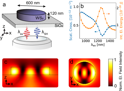
In Fig. 1 we demonstrate a finite-element simulation of a WS2 disk, that shows anapole-like behavior at an excitation wavelength of .
The hallmarks of the mode’s resonance, apart from its distinct near field pattern, are a dip in the far field scattering cross-section and an increase in the internal electric energy.
The latter is of particular interest for enhancing nonlinear effects.
If we choose the excitation wavelength to be at the anapole resonance, the resulting enhancement should be directly observable in the third order nonlinearity, as third harmonic (TH) generation has been shown to be more efficient in bulk than in few-layer TMDCs Wang et al. (2014); Khorasani (2018); Balla et al. (2018).
Until now, for second order effects the conversion efficiency is reported to be significantly weaker for bulk than for a few material layers Li et al. (2013); Zhao et al. (2016).
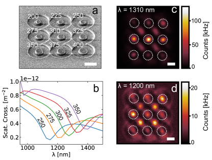
We use the results of our simulations to obtain a target parameter space and fabricate WS2 disks accordingly. For that, we exfoliate bulk WS2 on top of a glass substrate and pattern disks via focused ion beam (FIB) milling (for details see Supporting Information). In Fig. 2a we display a scanning electron microscope (SEM) image of individual disks, with radii spanning from to with increments of . We use TH generation as a characterization tool to test resonant field enhancement inside the disks. To this end, we scan over the resonators with excitation light and spectrally filter the emitted light via a dichroic beamsplitter and optical filters. The TH emission at is collected in the resulting transmission window at wavelengths below . According to simulated scattering curves (see Fig. 2b), a disk with a radius of around should exhibit the highest intensity enhancement by the anapole mode, as the resonance of this disk is closest to the chosen laser excitation wavelength. The experimental TH intensity map is displayed in Fig. 2c. Indeed the disk with a radius of exhibits the highest TH signal, whereas disks with smaller and larger radii show decreased TH emission (for spectra see Supporting Information). We thus indirectly map out the resonance profile of the enhancing mode. To confirm the wavelength dependent resonance behavior of our disks, we tune the excitation wavelength to . In the resulting TH intensity map (Fig. 2d) we now observe that disks with smaller radii are scattering stronger. In particular the disk with a radius shows the highest signal, again agreeing with the simulated scattering curves. The decrease in TH intensity for the lower excitation wavelength could be attributed to the higher absorption of WS2 at the corresponding TH wavelength of and the lower detection efficiency of the used detector. The observed TH scattering intensity dependence on the disk radius and on the excitation wavelength, combined with the discussed simulations, indicates that we have successfully built resonators that exhibit anapole-like behavior.
Having established the functionality of our nanoresonators, we now turn our attention to the main focus of this work, i.e. enhanced SH generation in resonant WS2 structures. First, we aim to develop a basic understanding of the physical processes at play. To theoretically describe the resonant SH emission we have to account for the overlap of the relevant electric fields inside the resonator. Those relevant fields are at the SH and at the fundamental wavelength. Following references Buckley et al. (2014); Lin et al. (2016) we express the emitted power at the SH wavelength as
| (1) |
where is the volume, is the vacuum permittivity, is the vacuum speed of light, is the fundamental wavelength in bulk, , are the absolute permittivities of WS2 at the respective wavelengths, is the incoming power of the excitation laser, is the coupling efficiency of to the fundamental resonator field , and is the second order susceptibility of WS2. According to Yan et al. (2018); Gigli et al. (2019) we can expand both the fundamental and SH fields in the WS2 disks in terms of quasinormal modes as
| (2) | |||
| (3) |
where is the SH wavelength in bulk, and are the modal excitation coefficients, which include the respective quality factors and coupling efficiencies, and are the quasinormal modes of the resonator at wavelength .
For instance, the resulting field intensity at the fundamental wavelength , displayed in Fig. 1, can be written as the sum of an electric dipole mode and a toroidal dipole mode Yang and Bozhevolnyi (2019); Savinov et al. (2019); Tian et al. (2019).
Please note, that reflects the modal overlap between the incoming field of the excitation laser and , whereas reflects the modal overlap between the excitation field and Yan et al. (2018); Gigli et al. (2019).
Having discussed the theoretical basis of SH generation in nanoresonators, we now study the measured SH response of our WS2 nanoresonators.
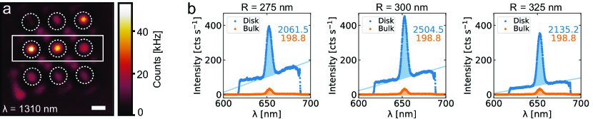
Figure 3a shows the SH intensity map of the disk array.
Here we use a new device, but the disk layout is identical to Fig. 2a, and the device shows the same TH behaviour as displayed in Fig. 2c.
At first sight, it appears that the disk with a radius of exhibits the highest SH signal.
However, when studying the spectra of the respective disks within the white box (see Fig. 3b) one finds that the radius of the disk with resonant SH generation is equivalent to the radius of the disk with resonant TH generation in Fig. 2c.
This is clear proof that the observed resonance behavior is indeed given by the resonance at the fundamental wavelength.
The discrepancy between the SH intensity map and the spectra results from the fact, that the map is recorded with an avalanche photo diode (APD) that integrates all the light that passes the optical filters.
Therefore unwanted incoherent background is recorded in addition to the coherent SH signal. The smaller background level for larger disks in Fig. 3b could stem from higher absorption due to the larger disk volume of large disks.
We next compare the SH signal from the radius disk with the SH signal originating from the unstructured bulk next to the disks .
We find a SH enhancement factor
| (4) |
where we account for the differences in excited area of the bulk measurement [given by the excitation beam’s intensity radius ] and the disk measurement (given by the disk radius ). Thus, by exploiting a resonance at the excitation wavelength, we successfully demonstrate a significant SH signal enhancement.
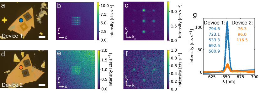
After having investigated the resonance behavior of single resonators, we now study the collective SH radiation of a closely spaced disk array. We use the same WS2 thickness () as for the single disk measurements (6% uncertainty). We choose the radius to be , as this leads to the strongest SH signal for an excitation wavelength of . The spacing between resonators is chosen to be . In order to illuminate a large area and thereby excite the whole disk array, we focus the incoming excitation of onto the back focal plane (BFP) of the 1.3 NA oil immersion objective used for imaging and signal collection. This results in a beam spot with a intensity diameter of . The average power on the sample is . For SH detection we image the spectrally filtered real space of the sample, as well as the BFP. Figure 4a and d show microscope images of two devices (devices 1 and 2) that were identically fabricated. The measured intensity maps are also displayed in Fig. 4 and reveal that the two devices drastically differ in their SH response. First, we observe a higher overall signal count in device 1 compared to device 2. Second, we find fundamentally different far field radiation patterns for the two devices. We note that these far field patterns are indicative of the individual antenna radiation patterns Milligan (2005); Balanis (2005) and allow us to differentiate between SH emission originating from the bulk or the surface of the disk resonators. In Fig. 4b (device 1) we observe the inner part of the disks lighting up (bulk emission) whereas in Fig. 4e (device 2) we observe the outer part of the disks lighting up (surface emission). This difference is even more pronounced in the recorded BFP images. Here we record a zeroth order emission lobe (central lobe) in Fig. 4c (device 1). Since a dipole emission pattern allows for a zeroth order emission lobe, the BFP image of device 1 suggests a dipolar SH emitter that originates from the bulk of the material. This emission lobe, however, is absent in Fig. 4f (device 2). Here, the BFP image reminds of the far field SH pattern of a gold rod array, cf. Busschaert et al. (2019), where the SH emission originates from the surface of the resonators. This surface emission suggests opposite dipoles with a phase difference of leading to destructive interference at an emission angle of 0°. We note that the SH emission behavior observed in device 2 is representative of other measured devices, also for devices with slightly varying bulk material thickness ( to ) or disk radius ( to ).
We have shown that we have fabricated WS2 resonator arrays which behave distinctly differently, despite identical fabrication parameters. The observed difference in SH emission can be explained by varying second order nonlinear properties () of equally thick (here around ) WS2 bulk material. In order to test this hypothesis, we measure the SH response from the non-structured regions of the WS2 which forms the material basis of the two presented devices, cf. Fig. 4g. The two respective regions are marked with circles in Fig. 4a,d. We see a drastic difference in SH signal strength between the two device materials. The SH signal of the bulk WS2 material 1 (material of device 1) is seven times stronger than the signal of the bulk WS2 material 2 (material of device 2). We also tested the polarization dependence by rotating the linear incoming polarization and measuring the respective SH response. The results are shown in Fig. 4g. The standard deviation over the mean is for bulk material 1 and for bulk material 2. We conclude that rotating the angle of the linear polarization leads to a negligible change in signal. To exclude the possibility that steps of single-layer WS2 on the surface of the disks are responsible for this difference in SH yield, we performed SH measurements on other WS2 bulk materials with measurable single-layer steps. We found that the signal difference (before and after step) was less than a factor of 2 (see Supporting Information).
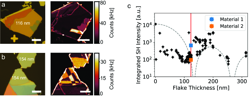
To get a deeper insight into the bulk material variations of our WS2 we conduct a statistical study of the material’s SH response as function of bulk thickness. Our findings are summarized in Fig. 5. In Fig. 5a and b we demonstrate two samples of WS2 bulk materials with spatially varying SH responses (see bright patches). The samples are left pristine after exfoliation (no further processing). We recorded high resolution atomic force microscope (AFM) scans to confirm that these samples are constant in thickness. Comparing bright and dark patches within one bulk material sample of constant thickness, leads to a difference in SH intensity of up to one order of magnitude. However, we also find that the SH yield depends on the bulk material thickness. In Fig. 5c we show the measured SH responses of bulk flakes with different thicknesses. We mark the average responses of the materials used for devices 1 and 2 discussed previously in Figs. 4 (see red line). Many samples with a thickness of have been measured most of which show a SH yield that agrees with the SH yield of device 2. Based on a simple phase matching model Boyd (2008), one would expect the integrated SH intensity of bulk WS2 to follow a sinc-function behavior
| (5) |
where corresponds to the integrated SH intensity of a monolayer, is the wave vector mismatch between the bulk SH wave vector and the bulk excitation wave vector . The thickness is weighted with a factor of 1.25 accounting for the high NA objective which increases the effective thickness seen by the light. The data shown in Fig. 5 roughly follows the theoretical sinc-like behaviour, but there is a significant number of outliers.
We propose three possible reasons (or a combination of those) for the measured differences in SH response: i) 3R polytypism, ii) stacking faults and iii) metallic phase changes. For a detailed discussion, see Supporting Information.
In conclusion we have demonstrated TMDC high-index resonators for nonlinear conversion enhancement. The resonance behavior of the bulk induced TH suggests the mode to be anapole-like. The assembly of our WS2 resonators into an array reveals the SH emission to originate either from the bulk or from the surface of the resonators, depending on variations in the SH response of the used bulk material. A statistical analysis indicates that most bulk flakes offer a small SH signal. As those flakes are used for fabricating resonators, we find that SH emission arises from the resonator surface. However, material outliers exhibiting an increased SH response can be utilized for resonators that show strong SH emission from the bulk of the resonators. We hypothesize that these material outliers are connected to stacking faults and/or polytypism. Clearly, further studies on material induced variations of SH generation in bulk TMDCs are needed.
Nevertheless, despite their presumed low bulk nonlinearity, we demonstrated the possibility to utilize bulk TMDCs for building resonant devices which exhibit highly efficient SH generation. The potential of our approach becomes clear as one compares the SH intensity of a WS2 monolayer (integrated SH intensity ) to outliers with bulk thicknesses between and (integrated SH intensity ), cf. Fig. 5c. By preselecting or engineering those highly efficient bulk flakes and patterning them into resonators, a resonantly enhanced SH intensity [see Eq. (4)] of could be achieved. Therefore, considering a unit area of the nonlinear material, resonantly enhanced SH generation from bulk TMDCs can be more than one order of magnitude more efficient than SH generation from the same TMDC in its monolayer form. Additionally the emitted SH power can further be enhanced by maximizing the overlap integral in Eq. (1) Carletti et al. (2015); Gigli et al. (2019). Practically this means that the resonator geometry needs to be optimized for maximal SH power Koshelev et al. (2020). Building on these results, preselecting and engineering TMDC bulk materials for maximal SH response, appears as an exciting venue for future research. Patterning those SH enhanced TMDCs into resonator arrays presents a profound opportunity for creating highly efficient nonlinear TMDC meta-surfaces which could be used for LIDAR Busschaert et al. (2019) and holographic imaging applications Gao et al. (2018).
Methods
Electrodynamic Simulations
Numerical simulations are carried out with the RF module of COMSOL Multiphysics. A single WS2 disk is defined on top of a glass substrate (), whereas the disk is surrounded by air () in the other half space. For the dielectric function of WS2 we use measured (in-plane) and calculated (out-of-plane) values Verre et al. (2019), which we linearly extrapolate towards higher wavelengths. The simulations are carried out in two steps: First, the resulting electric field of the geometry without disks is simulated under plane wave illumination. In a a second step, the disks are included in the simulation and starting from the targeted field is simulated. The two half spaces (above and below the glass-WS2 interface) are surrounded by perfectly matched layers (PMLs) to exclude back-reflection. In addition to the scattering cross-section we calculate the internal electric energy, see Fig. 1, by integrating the total internal electric field over the entire scattering volume,
| (6) |
where is the tensor of the absolute permittivity at the excitation wavelength.
Sample Fabrication
Glass cover slides with markers are prepared by ultrasonication in acetone with subsequent rinsing in isopropanol and deionized water. To remove all organic residues and to roughen the surface for better adhesion, the slides are then plasma-cleaned in 100 W oxygen plasma for 5 minutes. Now a sticky tape with exfoliated WS2 (bulk crystal provided by 2Dsemiconductors.com) is stamped on top of the glass slide and carefully removed. In the next step, suitable bulk material samples which sticked to the glass slide are identified via bright and dark field microscopy and their thickness is determined via an AFM measurement. The samples are then spin-coated with a conductive polymer (Espacer 300Z, 3000 rpm for 30s with 6s ramp) and baked at 115°C for 5 minutes. For nano-patterning we utilize a Gallium FIB system. The single disks are milled in a two step process: First, disks with a radius larger than the target radius are milled with a beam current of 7 pA. This higher beam current (large FIB radius) is used for a faster milling-rate. Second, a smaller beam current (small FIB radius) of 2 pA is employed for the final structure. The acceleration voltage is maintained at for every milling step. Regarding the arrays, the sample preparation before patterning is maintained as for the individual disks. To exclude any nonlinear signal from surrounding material, a WS2 area ( intensity diameter of the excitation beam) enclosing the array is removed. This is achieved by milling (with a 18 pA current) a square of x with a central exclusion area that is reserved for the array. Afterwards four point stars are milled (7 pA) into the left over WS2 area, such that WS2 pillars remain with the shape of octagons. In the last step disks with the final design radius are milled with a current of 2 pA. In contrast to individual disks, which are milled sequentially, arrays are milled in parallel. After patterning, the Espacer is washed off by rinsing the sample with deionized water for 2 minutes.
Nonlinear Measurements
Performing our nonlinear measurements we use the IR output of an optical parametric oscillator (Coherent Mira-OPO) that provides 200 fs pulses at a repetition rate of 76 MHz. To exclude any pump contributions we spectrally filter the laser (Semrock BL 1110LP, Chroma HHQ940LP).
The excitation and emission wavelengths are separated by a dichroic beamsplitter (DMSP950R by Thorlabs). Further spectral selection is implemented via optical filters (770SP, 650/60BP for SH generation, 561SP for TH generation at , 390/40BP for TH generation at , all filters by Semrock) in front of the detectors. The emitted optical signal is either sent on an avalanche photo detector (MPD PDM 50), on a spectrometer (Acton SP2300 with Pixis100 CCD) or on an EMCCD camera (Acton Photon Max 512). Different lens arrangements are used for real space and BFP imaging.
For confocal scanning experiments (Fig. 2, 3 and 5), the beam is directly focused onto the sample using an oil immersion objective (1.3 NA Plan Fluor Nikon). Due to underfilling, the resulting beam has a intensity radius of ( ) . Thus, it is larger than the maximal disk radius of . The average excitation power on the sample is measured to be ( ) for the excitation wavelength. The average power for the excitation wavelength is ( ) . The integrated SH intensity in Fig. 5c is calculated by determining the area under the recorded SH spectra.
For large area illumination (Fig. 4), the beam is sent through a lens ( focal length, AC254-400-C-ML by Thorlabs), that enables us to focus the laser onto the BFP of the objective. The resulting intensity diameter in the sample plane is roughly . For these measurements, the average power on the sample is .
To exclude the possibility that the reported varying SH bulk material responses are due to implanted ions or redistributed material (both from FIB process) or the Espacer, we conduct various tests. First, we find that the milling process generally reduces the SH signal (probably due to destruction of the underlying crystal), but does lead to a non-negligible increase in TH signal. Thus we cannot exclude that our TH measurements receive significant contributions from implanted ions. Second, redistributed material contributes at maximum to the total SH signal. Third, Espacer, when not washed away by deionized water, leads to a maximum SH signal increase of . All these possible influences cannot explain the 7 fold SH signal difference between bulk material 1 and 2. Thus, by exclusion and supported by the measurements displayed in Fig. 5c, we are left with the pure bulk nonlinearity as the reason for the observed SH signal difference.
Acknowledgements.
This work was financially supported by the Swiss National Science Foundation (grant no. 200021_165841). The authors thank E. Bonvin and N. Lassaline for valuable input during sample fabrication, and S. Papadopoulos for providing support during data analysis. We also would like to thank Dr. M. Timofeeva and F. Richter for providing help with simulations. We thank C. Gigli for enlightening discussions on quasinormal resonator modes. We thank Prof. A. Morpurgo and N. Ubrig for helpful discussions regarding TMDC crystal properties. Furthermore, the authors acknowledge the use of the facilities of the FIRST center of micro- and nanoscience and of ScopeM at ETH Zürich.Supporting Information
The Supporting Information includes:
sample fabrication; spectra of TH measurement; wavelength dependence of arrays; single layer dependence of SH signal; reasons for the measured differences in SH response.
References
- Kumar et al. (2013) N. Kumar, S. Najmaei, Q. Cui, F. Ceballos, P. M. Ajayan, J. Lou, and H. Zhao, Second harmonic microscopy of monolayer MoS2, Phys. Rev. B 87, 161403 (2013).
- Malard et al. (2013) L. M. Malard, T. V. Alencar, A. P. M. Barboza, K. F. Mak, and A. M. de Paula, Observation of intense second harmonic generation from MoS2 atomic crystals, Phys. Rev. B 87, 201401 (2013).
- Woodward et al. (2016) R. I. Woodward, R. T. Murray, C. F. Phelan, R. E. P. de Oliveira, T. H. Runcorn, E. J. R. Kelleher, S. Li, E. C. de Oliveira, G. J. M. Fechine, G. Eda, and C. J. S. de Matos, Characterization of the second- and third-order nonlinear optical susceptibilities of monolayer MoS2 using multiphoton microscopy, 2D Materials 4, 011006 (2016).
- Wang et al. (2018) Z. Wang, Z. Dong, H. Zhu, L. Jin, M.-H. Chiu, L.-J. Li, Q.-H. Xu, G. Eda, S. A. Maier, A. T. S. Wee, C.-W. Qiu, and J. K. W. Yang, Selectively plasmon-enhanced second-harmonic generation from monolayer tungsten diselenide on flexible substrates, ACS Nano 12, 1859 (2018).
- Chen et al. (2018) J. Chen, K. Wang, H. Long, X. Han, H. Hu, W. Liu, B. Wang, and P. Lu, Tungsten disulfide-gold nanohole hybrid metasurfaces for nonlinear metalenses in the visible region, Nano Letters 18, 1344 (2018).
- Hu et al. (2019) G. Hu, X. Hong, K. Wang, J. Wu, H.-X. Xu, W. Zhao, W. Liu, S. Zhang, F. Garcia-Vidal, B. Wang, P. Lu, and C.-W. Qiu, Coherent steering of nonlinear chiral valley photons with a synthetic Au-WS2 metasurface, Nature Photonics (2019).
- Day et al. (2016) J. K. Day, M.-H. Chung, Y.-H. Lee, and V. M. Menon, Microcavity enhanced second harmonic generation in 2D MoS2, Opt. Mater. Express 6, 2360 (2016).
- Yi et al. (2016) F. Yi, M. Ren, J. C. Reed, H. Zhu, J. Hou, C. H. Naylor, A. T. C. Johnson, R. Agarwal, and E. Cubukcu, Optomechanical enhancement of doubly resonant 2D optical nonlinearity, Nano Letters 16, 1631 (2016).
- Fryett et al. (2016) T. K. Fryett, K. L. Seyler, J. Zheng, C.-H. Liu, X. Xu, and A. Majumdar, Silicon photonic crystal cavity enhanced second-harmonic generation from monolayer WSe2, 2D Materials 4, 015031 (2016).
- Chen et al. (2017) H. Chen, V. Corboliou, A. S. Solntsev, D.-Y. Choi, M. A. Vincenti, D. de Ceglia, C. de Angelis, Y. Lu, and D. N. Neshev, Enhanced second-harmonic generation from two-dimensional MoSe2 on a silicon waveguide, Light: Science & Applications 6, e17060 (2017).
- Li et al. (2019) D. Li, C. Wei, J. Song, X. Huang, F. Wang, K. Liu, W. Xiong, X. Hong, B. Cui, A. Feng, L. Jiang, and Y. Lu, Anisotropic enhancement of second-harmonic generation in monolayer and bilayer MoS2 by integrating with TiO2 nanowires, Nano Letters 19, 4195 (2019).
- Yim et al. (2014) C. Yim, M. O’Brien, N. McEvoy, S. Winters, I. Mirza, J. G. Lunney, and G. S. Duesberg, Investigation of the optical properties of MoS2 thin films using spectroscopic ellipsometry, Applied Physics Letters 104, 103114 (2014).
- Li et al. (2014) Y. Li, A. Chernikov, X. Zhang, A. Rigosi, H. M. Hill, A. M. van der Zande, D. A. Chenet, E.-M. Shih, J. Hone, and T. F. Heinz, Measurement of the optical dielectric function of monolayer transition-metal dichalcogenides: MoS2, MoSe2, WS2, and WSe2, Phys. Rev. B 90, 205422 (2014).
- Krasnok et al. (2012) A. E. Krasnok, A. E. Miroshnichenko, P. A. Belov, and Y. S. Kivshar, All-dielectric optical nanoantennas, Opt. Express 20, 20599 (2012).
- Kuznetsov et al. (2016) A. I. Kuznetsov, A. E. Miroshnichenko, M. L. Brongersma, Y. S. Kivshar, and B. Luk’yanchuk, Optically resonant dielectric nanostructures, Science 354 (2016).
- Yang and Bozhevolnyi (2019) Y. Yang and S. I. Bozhevolnyi, Nonradiating anapole states in nanophotonics: from fundamentals to applications, Nanotechnology 30, 204001 (2019).
- Savinov et al. (2019) V. Savinov, N. Papasimakis, D. P. Tsai, and N. I. Zheludev, Optical anapoles, Communications Physics 2, 69 (2019).
- Tian et al. (2019) J. Tian, H. Luo, Y. Yang, F. Ding, Y. Qu, D. Zhao, M. Qiu, and S. I. Bozhevolnyi, Active control of anapole states by structuring the phase-change alloy Ge2Sb2Te5, Nature Communications 10, 396 (2019).
- Timofeeva et al. (2018) M. Timofeeva, L. Lang, F. Timpu, C. Renaut, A. Bouravleuv, I. Shtrom, G. Cirlin, and R. Grange, Anapoles in free-standing III–V nanodisks enhancing second-harmonic generation, Nano Letters 18, 3695 (2018).
- Miroshnichenko et al. (2015) A. E. Miroshnichenko, A. B. Evlyukhin, Y. F. Yu, R. M. Bakker, A. Chipouline, A. I. Kuznetsov, B. Luk’yanchuk, B. N. Chichkov, and Y. S. Kivshar, Nonradiating anapole modes in dielectric nanoparticles, Nature Communications 6, 8069 (2015).
- Baranov et al. (2018) D. G. Baranov, R. Verre, P. Karpinski, and M. Käll, Anapole-enhanced intrinsic raman scattering from silicon nanodisks, ACS Photonics 5, 2730 (2018).
- Grinblat et al. (2016) G. Grinblat, Y. Li, M. P. Nielsen, R. F. Oulton, and S. A. Maier, Enhanced third harmonic generation in single germanium nanodisks excited at the anapole mode, Nano Letters 16, 4635 (2016).
- Grinblat et al. (2017) G. Grinblat, Y. Li, M. P. Nielsen, R. F. Oulton, and S. A. Maier, Efficient third harmonic generation and nonlinear subwavelength imaging at a higher-order anapole mode in a single germanium nanodisk, ACS Nano 11, 953 (2017).
- Verre et al. (2019) R. Verre, D. G. Baranov, B. Munkhbat, J. Cuadra, M. Käll, and T. Shegai, Transition metal dichalcogenide nanodisks as high-index dielectric mie nanoresonators, Nature Nanotechnology 14, 679 (2019).
- Novotny and Hecht (2012) L. Novotny and B. Hecht, Principles of Nano-Optics, 2nd ed. (Cambridge University Press, 2012).
- Wang et al. (2014) R. Wang, H.-C. Chien, J. Kumar, N. Kumar, H.-Y. Chiu, and H. Zhao, Third-harmonic generation in ultrathin films of MoS2, ACS Applied Materials & Interfaces 6, 314 (2014).
- Khorasani (2018) S. Khorasani, Third-order optical nonlinearity in two-dimensional transition metal dichalcogenides, Communications in Theoretical Physics 70, 344 (2018).
- Balla et al. (2018) N. K. Balla, M. O’Brien, N. McEvoy, G. S. Duesberg, H. Rigneault, S. Brasselet, and D. McCloskey, Effects of excitonic resonance on second and third order nonlinear scattering from few-layer MoS2, ACS Photonics 5, 1235 (2018).
- Li et al. (2013) Y. Li, Y. Rao, K. F. Mak, Y. You, S. Wang, C. R. Dean, and T. F. Heinz, Probing symmetry properties of few-layer MoS2 and h-BN by optical second-harmonic generation, Nano Letters 13, 3329 (2013).
- Zhao et al. (2016) M. Zhao, Z. Ye, R. Suzuki, Y. Ye, H. Zhu, J. Xiao, Y. Wang, Y. Iwasa, and X. Zhang, Atomically phase-matched second-harmonic generation in a 2D crystal, Light: Science &Amp; Applications 5, e16131 (2016).
- Buckley et al. (2014) S. Buckley, M. Radulaski, J. Petykiewicz, K. G. Lagoudakis, J.-H. Kang, M. Brongersma, K. Biermann, and J. Vučković, Second-harmonic generation in GaAs photonic crystal cavities in (111)b and (001) crystal orientations, ACS Photonics 1, 516 (2014).
- Lin et al. (2016) Z. Lin, X. Liang, M. Lončar, S. G. Johnson, and A. W. Rodriguez, Cavity-enhanced second-harmonic generation via nonlinear-overlap optimization, Optica 3, 233 (2016).
- Yan et al. (2018) W. Yan, R. Faggiani, and P. Lalanne, Rigorous modal analysis of plasmonic nanoresonators, Phys. Rev. B 97, 205422 (2018).
- Gigli et al. (2019) C. Gigli, T. Wu, G. Marino, A. Borne, G. Leo, and P. Lalanne, Quasinormal-mode modeling and design in nonlinear nano-optics (2019), arXiv:1911.06373 [physics.optics] .
- Milligan (2005) T. A. Milligan, Modern Antenna Design (Wiley, 2005) p. 104.
- Balanis (2005) C. A. Balanis, Antenna theory: analysis and design (Wiley-Interscience, 2005) p. 286.
- Busschaert et al. (2019) S. Busschaert, N. Flöry, S. Papadopoulos, M. Parzefall, S. Heeg, and L. Novotny, Beam steering with a nonlinear optical phased array antenna, Nano Letters 19, 6097 (2019).
- Boyd (2008) R. W. Boyd, Nonlinear Optics (Elsevier, 2008).
- Carletti et al. (2015) L. Carletti, A. Locatelli, O. Stepanenko, G. Leo, and C. D. Angelis, Enhanced second-harmonic generation from magnetic resonance in AlGaAs nanoantennas, Opt. Express 23, 26544 (2015).
- Koshelev et al. (2020) K. Koshelev, S. Kruk, E. Melik-Gaykazyan, J.-H. Choi, A. Bogdanov, H.-G. Park, and Y. Kivshar, Subwavelength dielectric resonators for nonlinear nanophotonics, Science 367, 288 (2020).
- Gao et al. (2018) Y. Gao, Y. Fan, Y. Wang, W. Yang, Q. Song, and S. Xiao, Nonlinear holographic all-dielectric metasurfaces, Nano Letters 18, 8054 (2018).