Can surface-transfer doping and UV irradiation during annealing improve shallow implanted Nitrogen-Vacancy centers in diamond?
Abstract
It has been reported that conversion yield and coherence time of ion-implanted NV centers improve if the Fermi level is raised or lowered during the annealing step following implantation. Here we investigate whether surface transfer doping and surface charging, by UV light, can be harnessed to induce this effect. We analyze the coherence times and the yield of NV centers created by ion implantation and annealing, applying various conditions during annealing. Specifically, we study coating the diamond with nickel, palladium or aluminum oxide, to induce positive surface transfer doping, as well as annealing under UV illumination to trigger vacancy charging. The metal coated diamonds display a two times higher formation yield than the other samples. The coherence time varies by less than a factor of two between the investigated samples. Both effects are weaker than previous reports, suggesting that stronger modifications of the band structure are necessary to find a pronounced effect. UV irradiation has no effect on yield and times.
Nitrogen-vacancy (NV) centers have a great potential for quantum sensing. The spin of individual NV centers can be controlled and read out at ambient conditions by microwave and optical excitation Gruber et al. (1997). Many applications have already been demonstrated, such as imaging magnetometry Balasubramanian et al. (2008); Gross et al. (2017) and the recording of NMR spectra from molecular-size samples Staudacher et al. (2013); Mamin et al. (2013). Furthermore, small local temperature differences Neumann et al. (2013); Kucsko et al. (2013) and the movements of mechanical resonators Kolkowitz et al. (2012) can be measured.
For quantum sensing, close proximity of the NV center to the sample is crucial, which is only achieved for “shallow” NV centers located few nanometers beneath the diamond surface. A high control of the NV-surface distance can be achieved by implanting nitrogen atoms at low (keV) energies, followed by an annealing process to form NV centers. However, the resulting centers feature significantly reduced times () and a low () conversion yield between implanted nitrogen atoms and NV centers. This has been attributed to the formation of divacancies and higher order complexes, which compete with the NV formation and can act as paramagnetic defects or charge trapsFávaro de Oliveira et al. (2017).
By introducing a boron doped sacrificial layer in proximity to the implanted nitrogen layer, during annealing, times and the shallow NV center yield could be improved Fávaro de Oliveira et al. (2017). This phenomenon is explained by an increased hole density, leading to a positive charging of single vacancies, thus suppressing the formation of divacancies due to the repelling Coulomb forces. Recently, a significant improvement in the formation yield (from to over ) was achieved by directly n-doping the diamond with co-implanted phosphorous, oxygen or sulfur Lühmann et al. (2019). This success has been attributed to the same mechanism, except exploiting negatively charged single vacancies.
Both diamond doping and removal of a sacrificial layer are technically challenging and hence inaccessible to many laboratories. We therefore investigate whether similar effects can be achieved by technically simpler and noninvasive methods, in particular surface transfer doping and UV illumination.
Surface transfer doping is a method to induce a thin doped layer close to the diamond surface. It typically employs H-termination of the diamond to favor transfer of electrons across the surface into adsorbed electrolytes Maier et al. (2000), molecules Strobel et al. (2004), or metal electrodes Tachibana, Williams, and Glass (1992), inducing p-doping close to the surface. This technique has been previously employed to control the charge state of defects close to the surface Hauf et al. (2011); Schreyvogel et al. (2015).
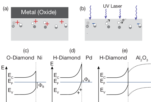
Here we aim to replicate the same effect by forming a nickel junction on O-terminated diamond as well as a palladium junction or aluminum oxide junction on H-terminated diamond. In contrast to previous work, we cannot employ a bare H-terminated surface, as it would not be stable throughout the annealing. Figure 1 summarizes the effects schematically.
For a coating of O-terminated diamond with nickel (Fig. 1a), the Fermi level of nickel is situated above the valence band, but below the Fermi level deep inside the diamond bulk. This latter level is expected to be set by the dominating impurity, substitutional nitrogen, to a level of Deák et al. (2014). By forming a junction between both materials, electrons will therefore diffuse into the diamond, to form a thermal equilibrium. This leads to the formation of a band bending within the diamond. The junction exhibits a Schottky barrier height , at the interface, between and Tsugawa et al. (2010); van der Weide and Nemanich (1994). Hence, vacancies in close proximity to the surface will be forced into the state. Neutral vacancies are known to have a higher mobility in the diamond than Davies et al. (1992); Deák et al. (2014), yet are believed to be more prone to clustering.
A H-terminated diamond surface induces an even stronger shift of the Fermi level, owing to the negative electron affinity of H-terminated diamonds Maier, Ristein, and Ley (2001). A junction with the metal palladium will shift the diamond Fermi level near the surface into the valence band, forming a thermally stable Ohmic contact with Wang et al. (2015). This will discharge vacancies close to the surface into a positive charge state (, ), possibly creating electrostatic repulsion between them Fávaro de Oliveira et al. (2017).
A similar situation is expected for an interface between diamond and the insulator aluminum oxide Al2O3, where a p-doped hole gas has been observed Kueck et al. (2010); Kasu, Sato, and Hirama (2012), and has been explored for power electronics in recent experiments Oi et al. (2018). The exact spatial dependence of band bending depends on several unknown parameters, in particular the dominating species and concentration of defects in the aluminum oxide, as well as the concentration of defects at the interface. Hence, no exact value for the barrier height can be given, making this case less well controlled than the metal contacts.
As a possible noninvasive and simple method to charge lattice defects, we investigated the effect of laser irradiation during the annealing process. We irradiated the diamond with a wavelength of (), biasing the vacancies into the negative charge state. The selected irradiation energy is located above the threshold required for conversion (reported to be Neves and Nazaré (2001)) and below the threshold for the inverse process (Neves and Nazaré (2001)). Ionizing other defects inside the diamond might lead to a further diffusion of charges influencing the diffusion of vacancies.
For this study, four IIa electronic grade (100) diamonds from Element Six Ltd. were used (size , , roughness ).
| D | D | D | D | |
|---|---|---|---|---|
| Applied Material | Nickel | Palladium | Al2O3 | |
| N-Implantation | ||||
| Piranha cleaning | ||||
| O-Plasma | ||||
| H-Plasma | ||||
| Annealing | + UV | |||
| Aqua regia | ||||
| Hydrofloric acid | ||||
| 3-acid-cleaning | ||||
| O-Plasma |
The main processing steps to form the NV centers in the individual samples are summarized in table 1. The diamonds were acid cleaned (4 hours in a boiling H2SO4:HNO3:HClO4 mixture) and jointly implanted with 15N+-ions (implantation energy , ion fluence ) at a angle (Cutting Edge Ltd.). We expect an implantation depth of Staudacher et al. (2012); Pezzagna et al. (2010).
The diamond samples D, D and D were oxygen terminated in an oxygen plasma (PS100-E, PVA TePla, , power ) for . D and D have been further fully hydrogen terminated by a hydrogen plasma in a microwave reactor (Astex, at (D) or (D), temperature )Dankerl et al. (2009).
films of nickel or palladium were deposited onto D and D by electron beam evaporation (, deposition rate: ) on the O- or H-terminated diamonds, respectively. Atomic layer deposition was used to grow a thick layer of aluminum oxide onto D (, p = ), with successive cycles of trimethylaluminum and water exposure. The diamonds were annealed in a vacuum of . After a heat up period, the diamonds were held for at . D was irradiated by a UV laser during the annealing process (, laser power , illuminated area ).
After annealing, the nickel and palladium layers were removed by an aqua regia solution. The aluminum oxide layer was removed by hydrofluoric (HF) acid. To remove the graphite layer resulting from the annealing, all diamonds were acid cleaned, as described above. The H-terminated diamonds D and D were finally O-terminated again.
The measurements of the spin properties of the NV centers were performed with a home-built confocal microscope. Excitation with a laser and imaging were performed through an oil-immersion objective (). The emitted photoluminescence was filtered by a long pass filter and measured by an avalanche photodiode. All measurements were performed at room temperature.
ODMR, Rabi and measurements were performed at a resonance frequency of , corresponding to a magnetic field . Lorentzian curves were fitted to the data obtained by ODMR measurements. The time was measured by Hahn echo sequences with a rabi frequency of . The data points were fitted to an ESEEM curve involving a stretched exponential decay, considering collapses and revivals induced by the 13C bath.
To relate the fluorescence properties and times of the samples, data of a diamond sample (denoted here as D) that was prepared using the standard annealing procedure was used from a previous studyBraunbeck et al. (2018).
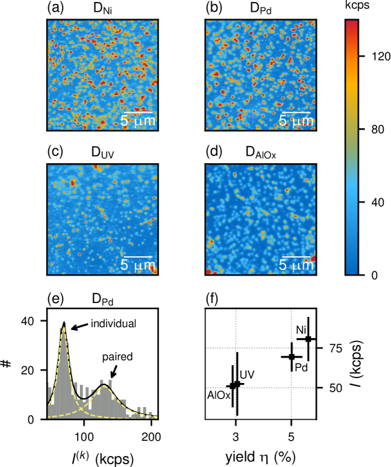
Figure 2a-d shows confocal fluorescence images of representative regions on the respective samples. We will analyze these images with regard to (i) fluorescence intensity of the individual NV centers, (ii) the density of NV centers, i.e. the conversion yield, and (iii) the background fluorescence intensity . Luminescence peaks (NV centers) of the fluorescence image are identified by points, which are maxima within a environment and a luminescence well above the background luminescence . The fluorescence intensity of individual NV centers is calculated by subtracting the background luminescence from the respective peak luminescence according to . Looking at the histogram of the luminescence intensities (Fig. 2e) we find a bimodal distribution. As we can only distinguish NV centers with a separation greater than the confocal volume, we attribute the peaks to individual (low-countrate) and pairs of (high-countrate) NV centers within the acquired resolution. This distribution was fitted to two Lorentzian peaks. In order to calculate the overall yield , a linear model was established, relating and using synthetic data of randomly distributed NV centers, with the true number of NV centers , the number of identified peaks and the respective integrated areas of the Lorentzian curves . With the assumption that the first peak is only attributed to single NV centers, we determine the mean fluorescence intensity of individual NV centers by the center of this peak, ignoring data points from the second peak. The result of this analysis is presented in table 2 and leads to the following results:
| (kcps) | (kcps) | () | (1) | |
|---|---|---|---|---|
| D | 15.3 | |||
| D | 8.7 | |||
| D | 10.2 | |||
| D | 1.9 | |||
| D | 8.5 |
The fluorescence intensity of individual NV centers is higher for the samples annealed under a metal coating (Ni and Pd) than for the samples annealed under Al2O3 coating and UV illumination. This hints towards a higher stability of the charge state in the metal-coated samples. Since our detection optics are selective for , discharging into the neutral state would manifest itself as a reduction of fluorescence intensity for this NV center.
The yield of NV center creation follows a similar trend. is given by the ratio of the density of formed NV centers to the density of implanted nitrogen atoms. In relation to D and D the yield is increased by for D and by for D to , as shown in Fig. 2f. Thus, by discharging V-, an increased NV center yield is seen within our samples.
The formation of paired NV centers seems to be correlated to the charge state of vacancies. The ratio relates the amount of paired NV centers in the measured samples (Fig. 2f) to the expected number from simulations. While annealing, the NV centers are dominantly in the negative charge state NV-. However, the vacancies may change their charge state due to surface doping, as they are in closer proximity to the surface. D, promoting positively charged vacancies (V+), has a increase of pairs compared to calculations (Tab. 2). Vacancies might be attracted by existing NV- centers, enhancing the formation of new NV centers in close proximity to other NV- centers. In D and Al2O3 no deviation from the expected value is observed, hence a random formation is achieved, with vacancies being in the neutral state (V0). The UV irradiated and the reference diamond have values well below 1, suggesting repulsion for negatively charged V-.
We observe that the type of termination during the annealing process does not appear to influence the brightness of the NV centers, as long as the H-terminated samples are O-terminated again after annealing. After the annealing and acid cleaning process, the NV center luminescence intensities in D and D were greatly reduced. In combination with a missing response on the microwave signal this suggests quenching of the NV centers into the neutral NV0 state. After the final O-Plasma treatment, the luminescence intensity increased to a similar level as found for non H-plasma treated diamonds, recovering the NV- state.
The background fluorescence intensity indicates the concentration of optically active lattice defects within the diamond and surface contamination. This value varies among the samples between (D) and (D). The particularly low background fluorescence of D might show a reduced defect concentration. Alternatively, the HF acid cleaning, which is necessary to remove the Al2O3 layer, might have removed further surface contamination, resulting in a reduced fluorescence of the nearby surface.
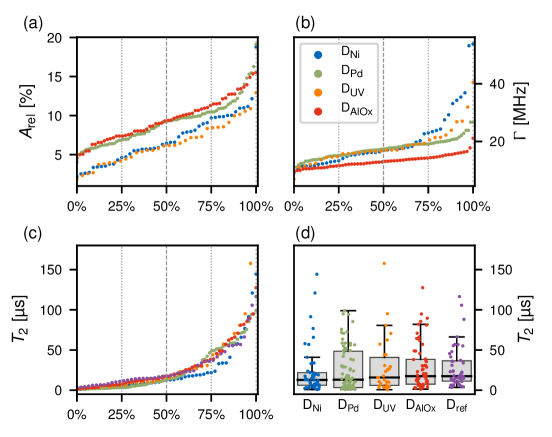
Figure 3 shows the distribution of relevant spin properties, where each dot represents an NV center: (a) the contrast of the optically detected magnetic resonance (ODMR) signal , (b) the ODMR linewidth , and (c,d) the spin coherence times . This analysis generates the following insights:
Fig. 3a illustrates that the observed ODMR contrast varies between the investigated samples. The NV centers of D and D show the highest ODMR contrast, which is about 50% larger compared to D and D. This is different from the behaviour observed in fluorescence properties, where D and D showed a comparable behaviour. Which seems to be due to the fact that the ODMR contrast is increased by several factors, most prominently a high stability of the state (D) and a narrow ODMR linewidth (D).
The linewidth of the ODMR spectra (Fig. 3b) is representative for the spin dephasing time . The linewidth is smallest for D, corresponding to the longest times. In addition, D and D show the narrowest distribution of . This suggests that the presence of a hole gas during annealing (or the oxygen plasma for removal of the hydrogen termination) improves . Roughly of the NV centers in D have a substantially increased linewidth .
The distributions of the times (Fig. 3c,d) show that the median values (corresponding to the values at 50% in Fig. 3c and indicated by black bars in Fig. 3d) vary only in a small range between (D) and (D, which also had the longest ). However, the tails of the distributions vary between the samples. For example, the upper quartile of the respective samples is moderately increased for D and halved for D in comparison to the three other samples. Both, the relatively large ODMR line broadening and the relatively narrow upper quartile of the D sample suggest some source of magnetic impurities. We speculate that even after the final etching process, a small concentration of residual nickel atoms with a strong magnetic moment could remain on the diamond surface, reducing the dephasing and coherence time of nearby NV centers. Nevertheless, as can be seen in Fig. 3c, in all samples the top of NV centers have similarly long values in the range between and . This shows that a small population of comparably robust NV centers exists in all investigated samples, which might be intrinsic to the diamond or lie deeper within the bulk.
In summary, we investigated UV illumination and surface transfer doping as tools to temporarily dope a diamond during the formation of implanted NV centers by annealing. As its most salient conclusion, our study reveals that these tools have a weaker effect on the conversion yield and the spin properties than doping by growth or co-implantation, however the effect is non-negligible. Conversion yields vary by a factor of two between samples, but have been demonstrated to vary by a full order of magnitude for co-implantation, using however less shallow NV centers, hence being more aided by the bulk properties. The coherence time also varies by less than a factor of two between our samples, but has been reported to improve by a full order of magnitude by temporary Boron doping. Additionally we have to note that the low magnitude of the effects and the small number of samples generate some sensitivity to systematic errors, such as different properties of the underlying diamond substrates, implantation regions or hydrogen contents. Nonetheless, we draw the following conclusions:
Coating the diamond by metals (nickel or palladium) results in an increased yield by a factor of two compared to the non metal coated samples, and partially induces enhanced paired formation of NV centers (palladium). It also improves the NV center fluorescence intensity, hinting towards a higher stability of the NV- charge state. The spin dephasing time improves significantly for an Al2O3 coating and slightly for a palladium coating, evidenced by a narrow ODMR linewidth, suggesting an effect of transfer doping, HF-treatment or the final O-plasma exposure. In contrast, the coherence time , arguably the most important figure of merit, is affected least strongly by our treatments. We observe a slight improvement for palladium coating and a clear reduction for nickel coating. The latter could be due to residual magnetic adsorbents or clustering of vacancies. Finally, UV irradiation has no effect on times and seems to degrade fluorescence intensity as well as .
Acknowledgements.
This work has been supported by the European Union (Horizon 2020 research and innovation programme, grant 820394 (ASTERIQS)) and the Deutsche Forschungsgemeinschaft (German Excellence Strategy – EXC-2111 – 390814868 and Emmy Noether grant RE3606/1-1). We thank Patrick Simon for hydrogen terminating samples of this study.Data Availability
Data available on request from the authors
References
- Gruber et al. (1997) A. Gruber, A. Dräbenstedt, C. Tietz, L. Fleury, J. Wrachtrup, and C. von Borczyskowski, Science 276, 2012 (1997).
- Balasubramanian et al. (2008) G. Balasubramanian, I. Y. Chan, R. Kolesov, M. Al-Hmoud, J. , C. Shin, C. Kim, A. Wojcik, P. R. Hemmer, A. Krueger, T. Hanke, A. Leitenstorfer, R. Bratschitsch, F. Jelezko, and J. Wrachtrup, Nature 455, 648 (2008).
- Gross et al. (2017) I. Gross, W. Akhtar, V. Garcia, L. J. Martínez, S. Chouaieb, K. Garcia, C. Carrétéro, A. Barthélémy, P. Appel, P. Maletinsky, J.-V. Kim, J. Y. Chauleau, N. Jaouen, M. Viret, M. Bibes, S. Fusil, and V. Jacques, Nature 549, 252 (2017).
- Staudacher et al. (2013) T. Staudacher, F. Shi, S. Pezzagna, J. Meijer, J. Du, C. A. Meriles, F. Reinhard, and J. Wrachtrup, Science 339, 561 (2013).
- Mamin et al. (2013) H. J. Mamin, M. Kim, M. H. Sherwood, C. T. Rettner, K. Ohno, D. D. Awschalom, and D. Rugar, Science 339, 557 (2013).
- Neumann et al. (2013) P. Neumann, I. Jakobi, F. Dolde, C. Burk, R. Reuter, G. Waldherr, J. Honert, T. Wolf, A. Brunner, J. H. Shim, D. Suter, H. Sumiya, J. Isoya, and J. Wrachtrup, Nano Letters 13, 2738 (2013).
- Kucsko et al. (2013) G. Kucsko, P. C. Maurer, N. Y. Yao, M. Kubo, H. J. Noh, P. K. Lo, H. Park, and M. D. Lukin, Nature 500, 54 (2013).
- Kolkowitz et al. (2012) S. Kolkowitz, A. C. B. Jayich, Q. P. Unterreithmeier, S. D. Bennett, P. Rabl, J. G. E. Harris, and M. D. Lukin, Science 335, 1603 (2012).
- Fávaro de Oliveira et al. (2017) F. Fávaro de Oliveira, D. Antonov, Y. Wang, P. Neumann, S. A. Momenzadeh, T. Häußermann, A. Pasquarelli, A. Denisenko, and J. Wrachtrup, Nature Communications 8, 15409 (2017).
- Lühmann et al. (2019) T. Lühmann, R. John, R. Wunderlich, J. Meijer, and S. Pezzagna, Nature Communications 10, 4956 (2019).
- Maier et al. (2000) F. Maier, M. Riedel, B. Mantel, J. Ristein, and L. Ley, Physical Review Letters 85, 3472 (2000).
- Strobel et al. (2004) P. Strobel, M. Riedel, J. Ristein, and L. Ley, Nature 430, 439 (2004).
- Tachibana, Williams, and Glass (1992) T. Tachibana, B. E. Williams, and J. T. Glass, Physical Review B 45, 11975 (1992).
- Hauf et al. (2011) M. V. Hauf, B. Grotz, B. Naydenov, M. Dankerl, S. Pezzagna, J. Meijer, F. Jelezko, J. Wrachtrup, M. Stutzmann, F. Reinhard, and J. A. Garrido, Physical Review B 83, 081304 (2011).
- Schreyvogel et al. (2015) C. Schreyvogel, V. Polyakov, R. Wunderlich, J. Meijer, and C. E. Nebel, Scientific Reports 5, 12160 (2015).
- Deák et al. (2014) P. Deák, B. Aradi, M. Kaviani, T. Frauenheim, and A. Gali, Physical Review B 89, 075203 (2014).
- Tsugawa et al. (2010) K. Tsugawa, H. Noda, K. Hirose, and H. Kawarada, Physical Review B 81 (2010), 10.1103/PhysRevB.81.045303.
- van der Weide and Nemanich (1994) J. van der Weide and R. J. Nemanich, Physical Review B 49, 13629 (1994).
- Davies et al. (1992) G. Davies, S. C. Lawson, A. T. Collins, A. Mainwood, and S. J. Sharp, Physical Review B 46, 13157 (1992).
- Maier, Ristein, and Ley (2001) F. Maier, J. Ristein, and L. Ley, Physical Review B 64, 165411 (2001).
- Wang et al. (2015) W. Wang, C. Hu, F. N. Li, S. Y. Li, Z. C. Liu, F. Wang, J. Fu, and H. X. Wang, Diamond and Related Materials 59, 90 (2015).
- Kueck et al. (2010) D. Kueck, A. Schmidt, A. Denisenko, and E. Kohn, Diamond and Related Materials NDNC 2009, 19, 166 (2010).
- Kasu, Sato, and Hirama (2012) M. Kasu, H. Sato, and K. Hirama, Applied Physics Express 5, 025701 (2012).
- Oi et al. (2018) N. Oi, M. Inaba, S. Okubo, I. Tsuyuzaki, T. Kageura, S. Onoda, A. Hiraiwa, and H. Kawarada, Scientific Reports 8, 10660 (2018).
- Neves and Nazaré (2001) A. J. Neves and M. H. Nazaré, Properties, Growth and Applications of Diamond (IET, 2001).
- Staudacher et al. (2012) T. Staudacher, F. Ziem, L. Häussler, R. Stöhr, S. Steinert, F. Reinhard, J. Scharpf, A. Denisenko, and J. Wrachtrup, Applied Physics Letters 101, 212401 (2012).
- Pezzagna et al. (2010) S. Pezzagna, B. Naydenov, F. Jelezko, J. Wrachtrup, and J. Meijer, New Journal of Physics 12, 065017 (2010).
- Dankerl et al. (2009) M. Dankerl, S. Eick, B. Hofmann, M. Hauf, S. Ingebrandt, A. Offenhäusser, M. Stutzmann, and J. A. Garrido, Advanced Functional Materials 19, 2915 (2009).
- Braunbeck et al. (2018) G. Braunbeck, S. Mandal, M. Touge, O. Williams, and F. Reinhard, Diamond and Related Materials 85, 18 (2018).