Achieving Minimal Heat Conductivity by Ballistic Confinement in Phononic Metalattices
keywords:
Ballistic transport, silicon metalattice, thermal conductivity, Time-domain thermoreflectance, first-principle calculationsThese authors contributed equally. \altaffiliationThese authors contributed equally.
1 Abstract
Controlling the thermal conductivity of semiconductors is of practical interest in optimizing the performance of thermoelectric and phononic devices. The insertion of inclusions of nanometer size in a semiconductor is an effective means of achieving such control; it has been proposed that the thermal conductivity of silicon could be reduced to 1 W/m/K using this approach and that a minimum in the heat conductivity would be reached for some optimal size of the inclusions. Yet the practical verification of this design rule has been limited. In this work, we address this question by studying the thermal properties of silicon metalattices that consist of a periodic distribution of spherical inclusions with radii from 7 to 30 nm, embedded into silicon. Experimental measurements confirm that the thermal conductivity of silicon metalattices is as low as 1 W/m/K for silica inclusions, and that this value can be further reduced to 0.16 W/m/K for silicon metalattices with empty pores. A detailed model of ballistic phonon transport suggests that this thermal conductivity is close to the lowest achievable by tuning the radius and spacing of the periodic inhomogeneities. This study is a significant step in elucidating the scaling laws that dictate ballistic heat transport at the nanoscale in silicon and other semiconductors.
2 Keywords
ballistic heat transport, Casimir limit, metalattice, phononic crystal, thermal conductivity, silicon
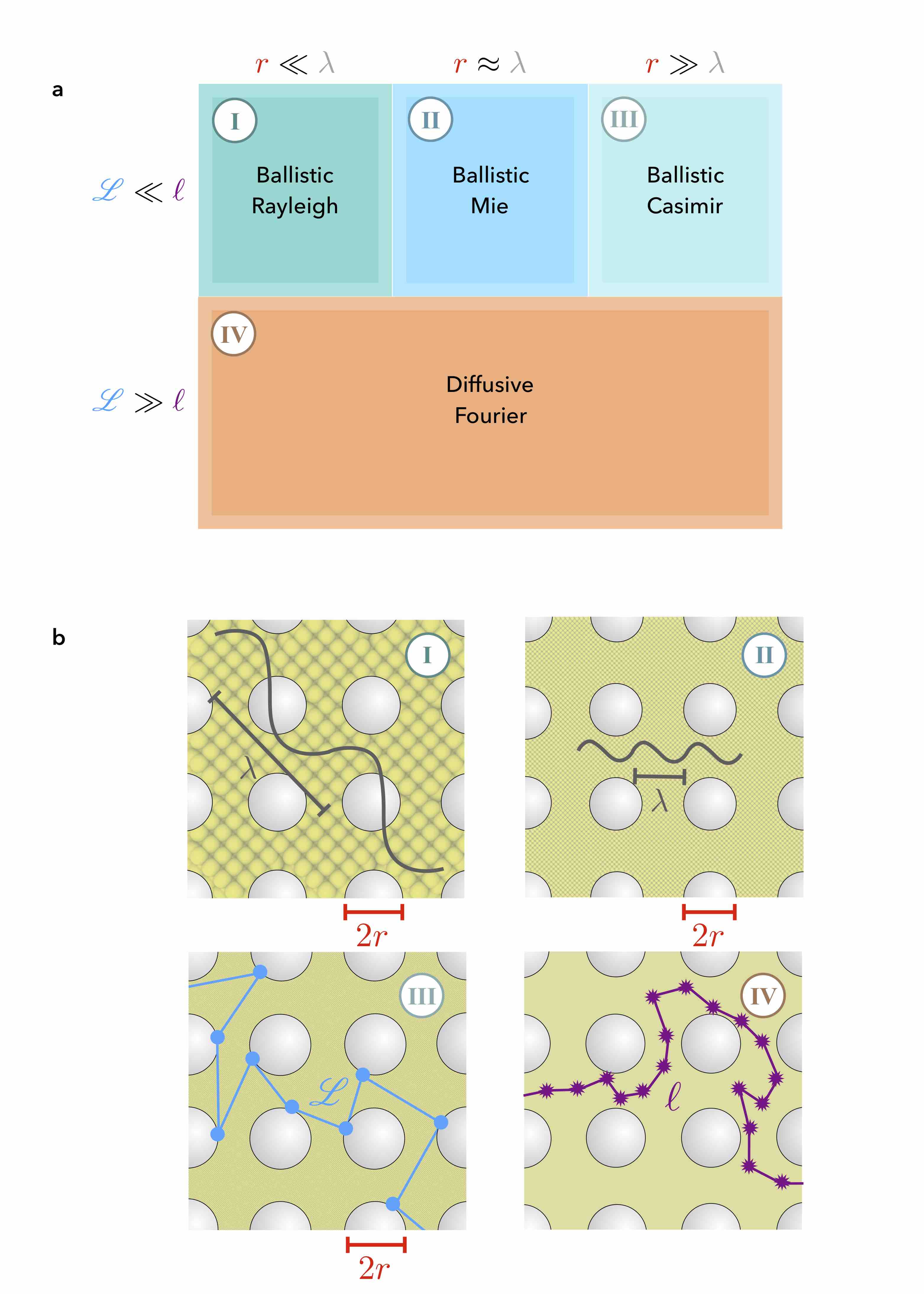
Ballistic transport occurs when the propagating waves do not diffract among themselves or against local defects, and as such is crucial to the performance of thermocrystal waveguides 1, the efficiency of thermoelectrics 2, 3, 4, the reliability of electronic devices that operate under cryogenic conditions 5 and the development of thermal diodes 6, 7, 8, 9. This regime of thermal transport is prevalent when the length scale associated with the confining network is shorter than the phonon mean free path . For a typical semiconductor of lattice heat conductivity , the mean free path can be estimated as (where is the Boltzmann constant, denotes the sound velocity, and is the volume of the unit cell comprising atoms), yielding 50-1,000 nm 10. Hence, a transition to the ballistic regime takes place when the length describing geometric confinement is brought down to a few tens of nanometers 11, 12, 13, 14, 1, 15.
It has been postulated that the dispersion of spherical inclusions smaller than 100 nm in a semiconducting matrix can lead to a thermal conductivity minimum. As shown in Fig. 1, in the Rayleigh limit where the radius of the spherical inhomogeneities vanishes (Regime i), the thermal conductivity decreases rapidly with according to the scaling law 16. Conversely, in the Casimir limit where the sphere size is very large in comparison to the incident wavelength (Regime iii), the thermal conductivity increases linearly with respect to sphere size: . 17, 11 At the juncture of these two trends (Regime ii), a minimum in the heat conductivity is expected 18, 19, 20.
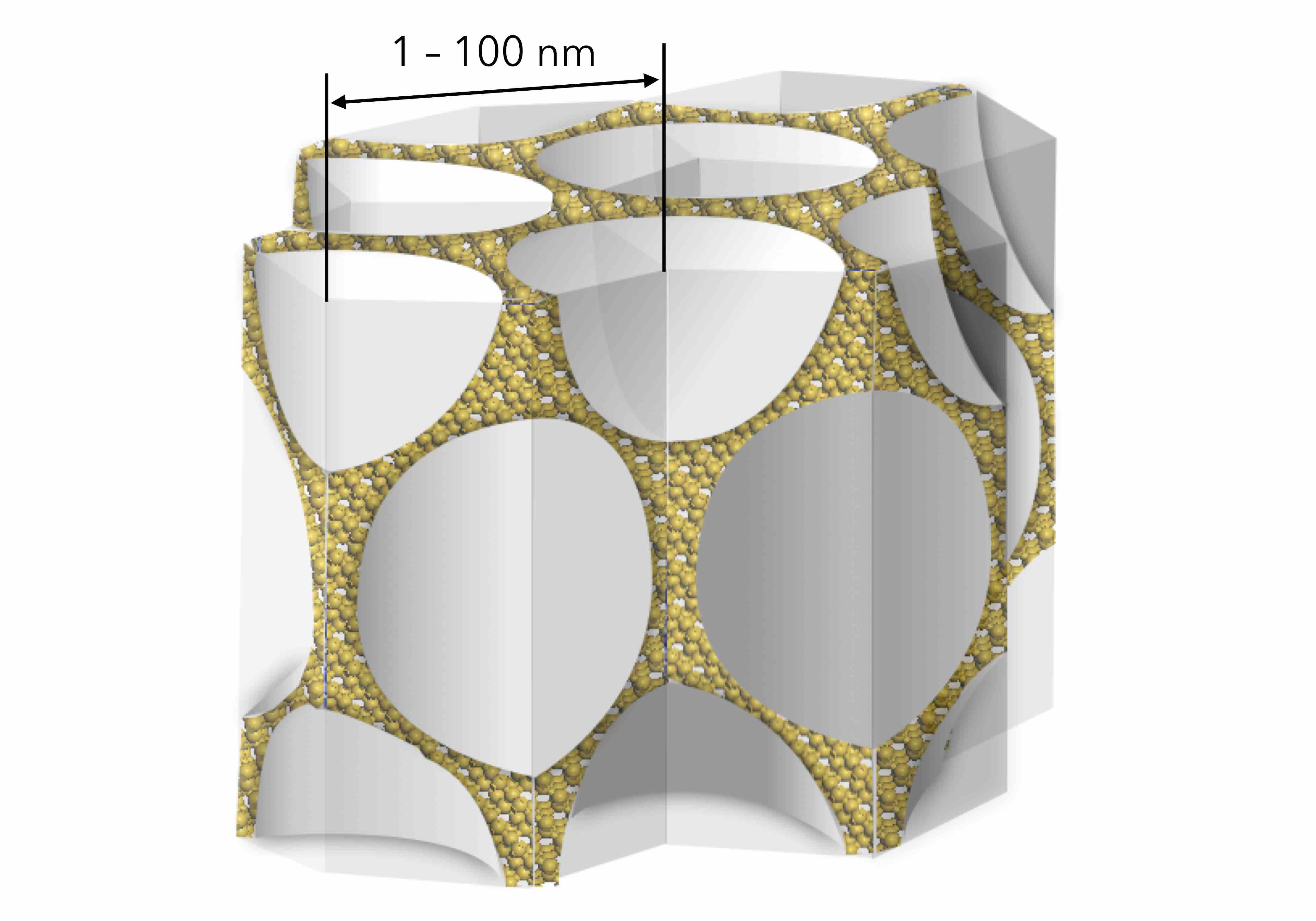
In this work, we aim to examine the possibility of this thermal conductivity minimum. To this end, we synthesize and characterize a class of metamaterials consisting of a periodic arrangement of nanometer-sized spherical inclusions in a semiconducting crystal (Fig. 2) 21, 22, which we refer to here as metalattices. Similar nanostructures have been synthesized previously, by means of conventional chemical vapor deposition, albeit on a scale that is an order of magnitude larger 23, 24, 25, 26. In this work, silicon metalattices with sphere radii in the range of 7 to 30 nm are obtained by high-pressure infiltration and selective etching of colloidal templates 27. We undertake a comprehensive experimental and theoretical study of the thermal conductivity of metalattices, with a focus on verifying and explaining the occurrence of a minimal lattice thermal conductivity as a function of size, volume fraction, and the content of the spherical inclusions.
3 Results and discussion
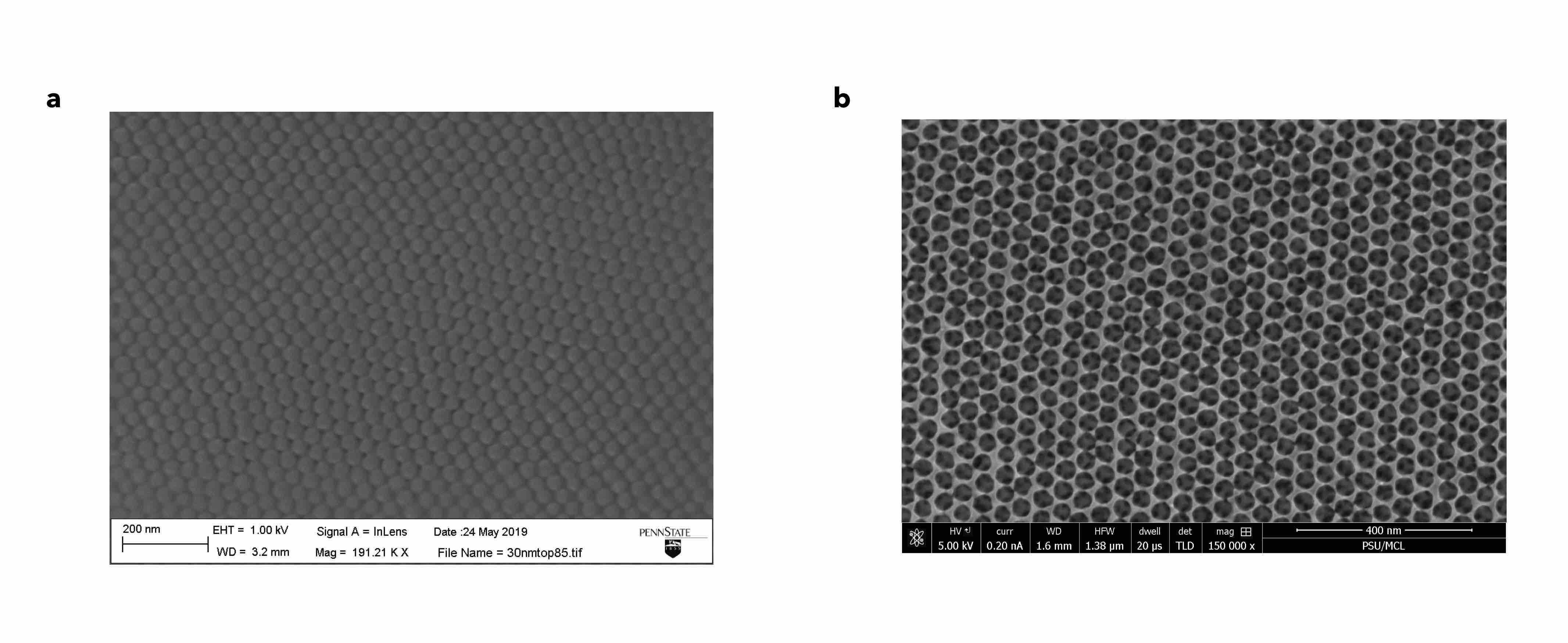
Two types of silicon metalattices are synthesized: one with empty pores and one with silica filled pores. While a number of studies have focused on synthesizing and investigating thermal transport in two-dimensional nanoporous systems 28, 29, 30, 31, 32, 1, 33, there are limited reports on the thermal transport of three-dimensional metalattice (or inverse opal) nanostructures23, 24, 25, 26. It should be noted that the sizes of the spheres of previously reported structures are in the range of 100 to 1,000 nm. Here, in order to probe the size regime that potentially achieves minimal thermal conductivity, silicon metalattices with sphere radii from 7 to 30 nm are synthesized by infiltrating the interstitial voids of an ordered template assembled from silica nanospheres by means of high-pressure confined chemical vapor deposition (HPcCVD)34, 35, 36. Using a similar method, magnetic metalattices with average sphere radius as small as 15 nm have been previously synthesized27. The synthesis of silicon metalattices starts with making a colloidal solution of mono-dispersed silica nanospheres, using the seeding and regrowth process described by Hartlen et al. 37 and Watanabe et al. 38. These silica spheres are subsequently assembled as closely packed templates on a silicon substrate using vertical deposition techniques 39, 40. In this method, after cleaning the silicon substrate using a Piranha solution, the sample is placed with an inclination angle of approximately 30 degrees in a vial that contains a colloidal suspension formed by diluting the above-prepared silica nanoparticles. Subsequently, the vial is placed in an oven where the solvent evaporates off under controlled temperature and humidity conditions, leaving behind a silica template film on the substrate. Depending on sphere size and deposition conditions, the thicknesses of these films vary from 250 to 2,000 nm, as observed from electron microscope imaging. The template film is further calcined at 600 to remove the remnant organic contamination. Voids of this template film are then infiltrated with silicon using high-pressure confined chemical vapor deposition. Deposition time is adjusted for each sample such that a silicon over-layer is formed on the top of the template. This ensures complete void filling of the structures. After removing this over-layer using deep reactive ion etching, the infiltrated amorphous silicon is crystallized by annealing at 800 oC for 30 minutes under an inert atmosphere. A scanning electron microscope image of the resulting silica-filled silicon metalattice with an average sphere radius of 15 nm is shown in Fig. 3(a). To make silicon metalattices with empty pores, the silica-filled metalattices are etched with a vapor of 49% hydrofluoric acid. The resulting empty silicon metalattice is shown in the scanning electron microscope image of Fig. 3(b).
Thermal conductivity measurements are performed using time domain thermoreflectance (TDTR) 41, 42, 43. All measured samples are deposited with aluminum as a transducer layer using electron beam evaporation 44, 45, with thicknesses ranging from 80 to 120 nm as determined using picosecond acoustics. We measure 4-5 different spots on each sample for room temperature thermal conductivity data (the experimental procedure and parameters are detailed in the Methods section). Low temperature thermal conductivity measurements are performed with the samples loaded inside a liquid helium continuous flow optical cryostat, providing temperature stability within 1 K.
| Type | Temperature | Radius | ||||
|---|---|---|---|---|---|---|
| 7 nm | 10 nm | 15 nm | 30 nm | |||
| Filled | 140 K | 1.11 0.08 | 0.79 0.05 | 1.45 0.09 | 1.51 0.08 | W/m/K |
| 200 K | 1.26 0.09 | 0.91 0.06 | 1.69 0.11 | 1.74 0.10 | ||
| 300 K | 1.33 0.09 | 0.94 0.06 | 1.68 0.11 | 2.08 0.12 | ||
| Empty | 300 K | 0.16 0.05 | 0.24 0.04 | 0.26 0.07 | ||
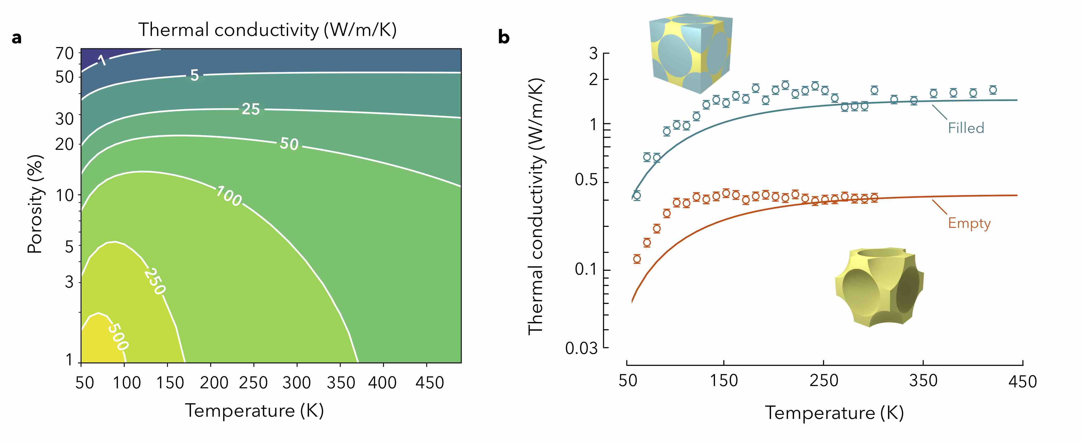
The experimentally measured thermal conductivities are reported in Table 1. From 140 to 300 K, the thermal conductivities of filled metalattice samples show a minimum as a function of the sphere radius. However, such a minimum is not found in empty silicon metalattices: the thermal conductivity increases with increasing sphere sizes. On the other hand, it is observed that the thermal conductivities of empty metalattices are ten times smaller than the filled ones, with the lowest value being 0.16 W/m/K. In order to understand the influence of sphere content (empty or filled), we develop and validate a computational model based on the Casimir theory of ballistic transport.
In this model 46, the heat current density at an arbitrary point can be expressed as
| (1) |
where and are the frequency and group velocity of the phonon with wave vector , polarization , and statistical occupancy , with the sum being carried out over a sampling of wave vectors in reciprocal space. Here, defines the area that is ballistically accessible from the point and is the total solid angle associated with . For small temperature gradients, Eq. (1) can be recast as
| (2) |
with being the phonon heat capacity. The heat flux across a surface area is then calculated as
| (3) |
Here, is a unit vector antiparallel to the temperature gradient (and where use has been made of the fact that ). Since the temperature gradient is small, the change in the heat capacity from the emitting surface to the receiving area is negligible, so that both the heat capacity and the group velocity of the phonon can be taken out of the integral. We thus obtain an expression for the heat conductivity that is reminiscent of the solution to the linearized Boltzmann transport equation:
| (4) |
where the ballistic length reads
| (5) |
with
| (6) |
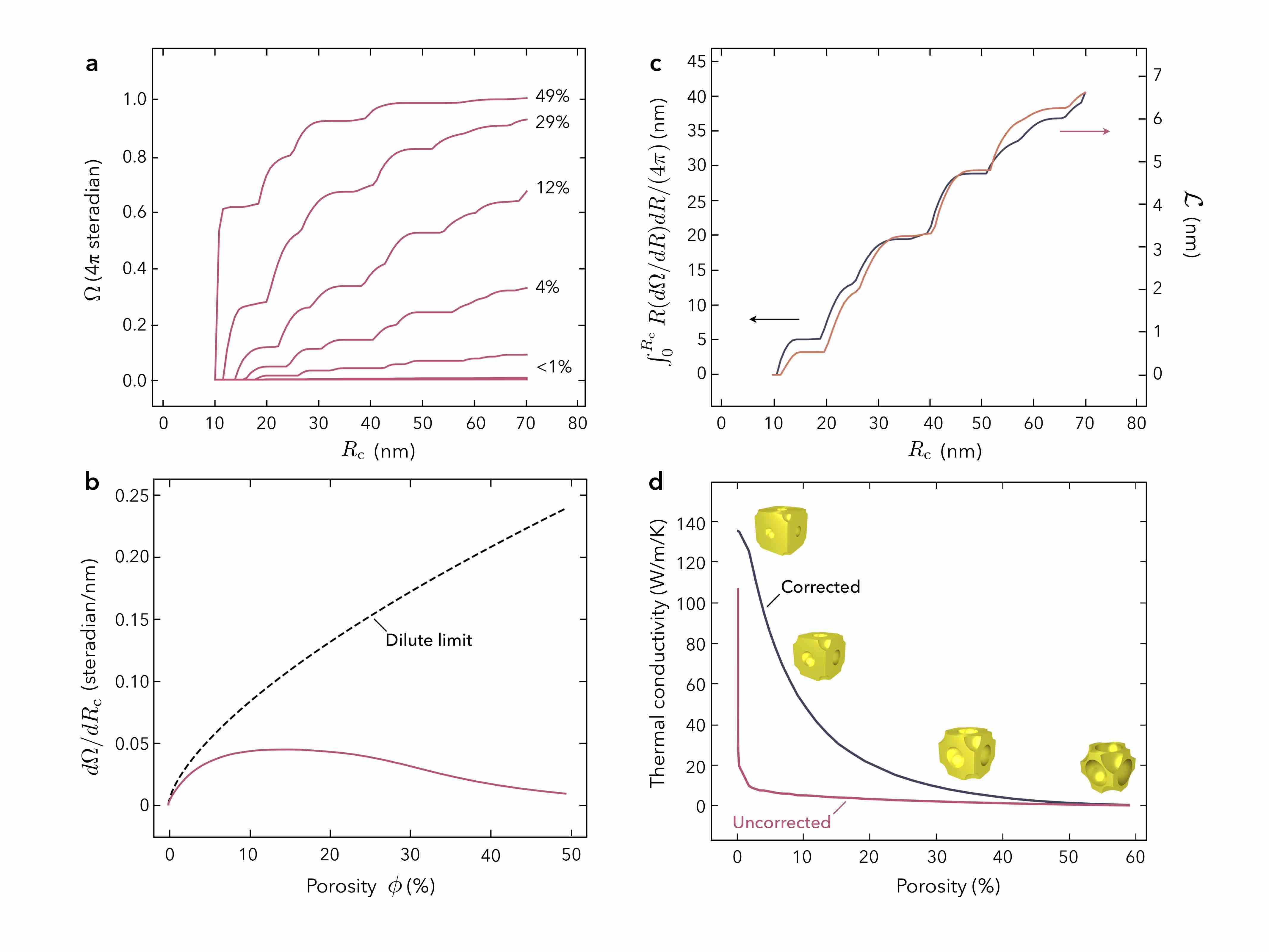
The calculation of the mean free path necessitates a simulation domain of finite size. Here, we adopt a spherical truncation of cutoff radius . Figure 4 examines the influence of this truncation on the convergence of the calculated ballistic length . As one might expect, when the porosity is small, the total solid angle captured inside the simulation domain is significantly lower than steradians, as shown in Fig. 4(a). To restore the omitted contribution, we develop a model that consists of including the solid angle beyond by estimating the distance at which the solid angle reaches steradians . The slope of the solid angle at is shown in Fig. 4(b). In the dilute regime where the pores are small and well separated, each pore contributes the same amount of solid angle (neglecting shadowing effect). In this limit, the slope can be expressed as , where is the period of the metalattice. It is then possible to obtain the corrected ballistic length scale from the uncorrected value :
| (7) |
where is the geometric factor that relates to its angular-averaged approximation, as shown in Fig. 4(c). The thermal conductivities of metalattices calculated with and without long-range correction are compared in Fig. 4(d), showing the importance of this corrective procedure in computing the ballistic length scales at low porosity. The procedure we proposed can be used to study thermal transport in the dilute limit in other phononic systems such as two-dimensional phononic nanostructures, and can be implemented easily within other numerical approaches such as Monte Carlo calculations 47, 48, 49, 50.
We now apply this model to determine the thermal conductivity of metalattices. The vibrational spectra and phonon-phonon mean free paths are derived from semilocal density-functional theory. The effect of Rayleigh scattering on ballistic transport is included through the rescaling , in which describes the subwavelength enhancement of the ballistic cross section (the scattering efficiency) 51, 16. The calculations of the scattering efficiency, the effect of Brillouin zone folding on phonon group velocity, as well as the effect of phonon-isotope scattering are discussed in the Supplementary Information.
Figure 5(a) reports the thermal conductivities of filled metalattices as a function of porosity and temperature. In the low porosity limit (1%), the thermal conductivity decreases with increasing temperature, a behavior that is reminiscent of bulk silicon. However, in the high-porosity limit (70%), the thermal conductivity shows a trend that is characteristic of ballistic phonon transport12, 15, 13, 14, 1, 11; increases gradually as the temperature is raised from 50 to 250 K, before reaching a maximum. Experimental measurements on samples with the same geometric parameters exhibit a similar saturation [Fig. 5(b)], thereby providing clear evidence that ballistic transport is prevalent in silicon metalattices. This trend has been previously predicted in two-dimensional metamaterials. 12 Compared to the two-dimensional case, the thermal conductivities of metalattices are reduced to much lower values due to a sharper decrease in the scattering cross section in higher dimension. Moreover, while the asymptotic values of thermal conductivity at room temperature are relatively well predicted by the ballistic model, there is a larger discrepancy between theory and experiment at lower temperature (50 to 150 K) for the empty metalattices. This discrepancy is likely due to specular scattering, which causes an increase in the phonon ballistic mean free paths.52 This effect is more pronounced for long wavelength phonons that dominate heat transport at low temperatures.53, 54
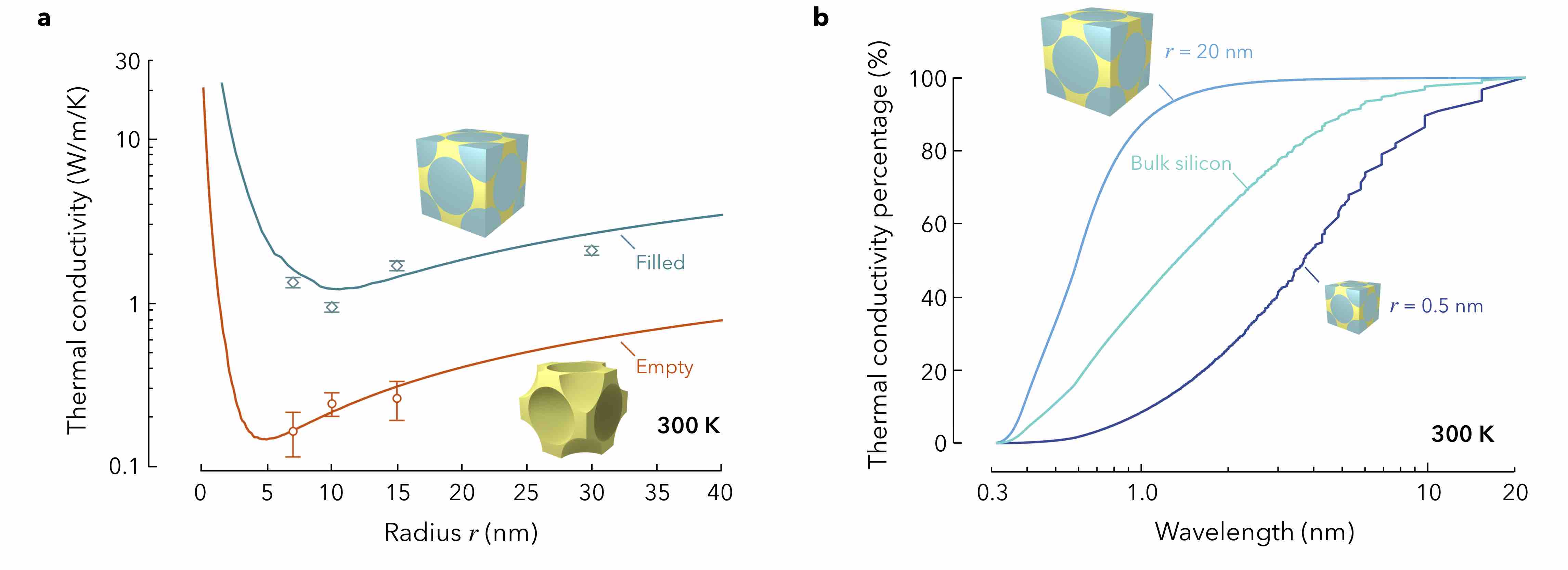
In Fig. 6(a), we investigate the thermal conductivities of metalattices as a function of pore radius. Our model reveals that the occurrence of the thermal conductivity minimum depends on the content of the inclusions: for silicon metalattices with empty and silica-filled spheres, simulations predict a thermal conductivity minimum at a composition-dependent radius (5 nm for empty metalattices and 10 nm for filled metalattices). Experimental measurements strongly suggest the existence of a minimal heat conductivity in filled silicon metalattices, but not in empty metalattices. Our simulation points out that an even smaller sphere radius is needed to reach the minimal thermal conductivity in empty metalattices. The thermal conductivity predictions from our model are in quantitative agreement with experimental measurements, implying that ballistic transport is likely responsible for the considerably reduced conductivity of silicon metalattices. We note that the current implementation of the ballistic model is based on finite-element discretization, where the surfaces of the pores are kept rigid. Investigating the effect of local surface distortion could potentially increase the reliability of the present calculations. Moreover, we note that the theoretical predictions are based on perfect metalattice structures, while there exist small deviations in the size, shape and dispersity of the pores experimentally. Taking these effects into consideration is a relevant topic for further theoretical development.
In Fig. 6(b), we examine the different ballistic regimes by decomposing the thermal conductivity of metalattices onto a wavelength spectrum. We consider two face-centered cubic metalattices with different radii, namely, 0.5 nm and 20 nm. The wavelength-decomposed thermal conductivity of bulk silicon is also plotted for reference. It is shown that the two metalattices show distinct behaviors, i.e., phonons that mainly contribute to the thermal conductance in metalattices with small pores (0.5 nm) have long wavelengths due to Rayleigh scattering, whereas 90% of heat propagation through metalattices with large pore size (20 nm) is facilitated by phonons with extremely short wavelengths (smaller than 1 nm), corresponding to the Casimir regime. Figure 6 demonstrates the possibility of adjusting the sphere sizes to filter out specific wavelengths and achieving sensitive control over thermal transport.
In closing, we discuss the practical significance of the observed thermal conductivity minimum. Potential applications of the geometry-dependent thermal conductivity of phononic metalattices include the design of thermal rectifiers. By incorporating inclusions of different sizes across a semiconductor, different regions of the material could have different temperature-dependent thermal conductivities. This spatial gradient of pore radii will result in a drastically different effective thermal resistance depending on the direction of the temperature bias. The thermal rectification performance of graded metalattices using various semiconductors is currently being studied and could ultimately enable the realization of efficient thermal diodes.
4 Conclusion
We have investigated thermal transport in silicon metalattices to verify the existence of a thermal conductivity minimum as a function of the radius of the spherical inclusions. Thermal conductivity measurements in silica-filled silicon metalattices strongly imply the occurrence of this minimum when the radius of the pore is brought down to 10 nm in the close packing limit. The thermal conductivity of empty metalattices is shown to be as small as 0.16 W/m/K for a sphere radius of 7 nm. Using a well-converged phonon ballistic model, we have found indications that the thermal conductivity may be further lowered by reducing the sphere radius to 5 nm. This work highlights the potential of metalattices as a widely applicable platform to minimize the thermal conductivity of crystalline semiconductors, motivating further work to push the frontier of nanofabrication into the Rayleigh limit of heat transport.
5 Methods
Finite-element simulations. Finite-element models are constructed to compute ballistic mean free paths using python and the trimesh module 55. Spherical inclusions are modeled by two-dimensional surface triangular meshes, and a ray-casting algorithm is employed to find the accessible areas for ballistic propagation. Each spherical surface mesh contains 2,068 triangular elements. The cutoff radius is chosen so that at least 200 explicit spheres are included in the simulation. The longitudinal and transverse scattering efficiencies are computed according to Kraft and Franzblau 51, Ying and Truell 16. The density, Poisson’s ratio, and Young’s modulus are taken to be , , GPa for silicon, and , , GPa for silica.
First-principles simulations. The force constant matrix is obtained from density-functional theory calculations using a 3 3 3 point mesh. Self-consistent calculations are done using the Perdew-Burke-Ernzehof approximation with the pw code of the Quantum-Espresso software package 56, 57. Norm-conserving pseudopotentials are used with kinetic energy cutoffs of 100 and 400 Ry. The Brillouin zone is sampled with a 3 3 3 Monkhorst-Pack grid 58. Phonon relaxation times are computed using the phono3py package based on the computed harmonic and anharmonic force constants 59. The resulting bulk thermal conductivity of silicon at 300 K using a -point extrapolation is 135 W/m/K, in good agreement with the experimental value 60.
Time-domain thermoreflectance measurements. Time-domain thermoreflectance (TDTR) is applied to measure the thermal conductivity of the silicon metalattices. A titanium-sapphire laser centered at 800 nm wavelength and emitting 100 fs pulses at a repetition rate of 80 MHz is used. The emitted beam is divided into pump and probe beam paths using a polarizing beam splitter with a half waveplate controlling the power distribution in the two beam paths. The pump beam is modulated by a square wave at a frequency MHz using an electro-optic modulator, which serves as the reference frequency for signal collection by the lock-in amplifier. It is then passed through a bismuth borate crystal to convert its wavelength from 800 nm to 400 nm using second harmonic generation. Color filters are placed before the detector to help prevent any spurious signal contribution from the scattered pump beam at the modulation frequency. The probe beam is sent through a delay stage that can provide a maximum time delay of 6 ns with respect to the pump beam. Both beams are then coaxially focused through a 5-magnification microscope objective onto the sample surface. The focal spot sizes used in the system are 21 m for the pump beam and 5-10 m for the probe beam as measured by knife edge technique. A complementary metal-oxide semiconductor (CMOS) camera is used in this setup to create a dark field image of the sample surface during each measurement. The pump beam absorbed by aluminum on the sample surface creates a modulated surface heating, and the temperature decay is monitored by a time-delayed probe beam reflectivity. The reflected beam is focused through a lens onto a silicon photodiode detector. It is connected to a wide (RF) lock-in amplifier via a resonant (RLC) circuit which collects the in-phase component and out-of-phase component of the thermoreflectance signal as a function of delay time at a resonance corresponding to the modulation frequency. The schematic describing the experimental setup for the time-domain thermoreflectance measurement is available in the Supplementary Information.
We measure at least 4 different spots on each sample for room temperature thermal conductivity data. While fitting the experimental ratio to the thermal model, eight unknown parameters, namely, the thermal conductivity of the silicon substrate (), volumetric heat capacity of the silicon substrate (), thermal conductivity of aluminum (), volumetric heat capacity of aluminum (), interfacial thermal conductance between aluminum and the metalattice film (), and interfacial thermal conductance between the metalattice film and the silicon substrate (), thermal conductivity of the film (), and volumetric heat capacity of the film () need to be determined. Amongst these, literature reported values are taken for the thermal conductivity and volumetric heat capacity of aluminum and silicon, respectively. 61 The heat capacity of the metalattice film is calculated using the rule of mixtures , where is the volume fraction of the pores in the metalattice film and and are the volumetric heat capacities of pore material and silicon. Thus, for filled metalattices, is taken as the literature reported value for the volumetric heat capacity of silica. For empty metalattices, the first term is neglected due to the negligible volumetric heat capacity of air with respect to silicon. The sensitivity analysis of experimental parameters, as well as the original room temperature time-domain thermoreflectance measurement data for empty and filled metalattices at different sphere sizes, are included in the Supplementary Information.
The thermal penetration depth in the samples is estimated from
| (8) |
where is the modulation frequency of the pump beam 62, 63, which yields penetration depths of 100-300 nm in the temperature range of 30-300 K for all metalattice samples. We use reasonable estimates for thermal conductivity and heat capacity for the metalattice film. Since the length scale in all cases is much smaller than the spot sizes used in the measurement, the contribution from radial conduction is ignored and thermal transport is considered one-dimensional.
Experimentally, the total laser power incident on filled metalattice samples is 65 mW at room temperature and is reduced to 6 mW at 30 K. For empty metalattice samples however the total power is taken as 40-50 mW at room temperature and reduced to 5 mW at 30 K. As a result, the temperature change due to steady-state heating is estimated to be
| (9) |
where is the reflectivity of aluminum, and and are the sizes of the pump and probe spots, respectively 64, 65. In our setup, the temperature rise for all the samples in 30-300 K range is smaller than 1 K. This ensures the validity of both the single-temperature approximation and the condition of linear reflectance change.
Appendix A Supporting Information
The Supporting Information is available free of charge on the ACS Publications website at (…). The following supplementary content is provided: the experimental setup for the time-domain thermoreflectance measurements, the theoretical discussion of the ballistic length scales (self-diffusion and driven diffusion), the thermal conductivity calculation using the ballistic model with a benchmark application for silicon thin films, the calculation of the Rayleigh scattering efficiency, the reduction of the phonon group velocity in metalattices, and the discussion of phonon-isotope scattering effects.
Appendix B Acknowledgements
The authors acknowledge financial support from the National Science Foundation Materials Research Science and Engineering Center for Nanoscale Science at Penn State University under grant NSF-DMR 1420620.
The authors dedicate this contribution to the life and memory of John V. Badding.
Appendix C Table of Content Image
![[Uncaptioned image]](/html/2004.14915/assets/new_TOC.jpg)
References
- Anufriev et al. 2017 Anufriev, R.; Ramiere, A.; Maire, J.; Nomura, M. Heat Guiding and Focusing Using Ballistic Phonon Transport in Phononic Nanostructures. Nat. Commun. 2017, 8, 15505
- Schierning 2014 Schierning, G. Silicon Nanostructures for Thermoelectric Devices: A Review of the Current State of the Art. Phys. Status Solidi 2014, 211, 1235–1249
- Boukai et al. 2008 Boukai, A. I.; Bunimovich, Y.; Tahir-Kheli, J.; Yu, J.-K.; Goddard, W. A.; Heath, J. R. Silicon Nanowires as Efficient Thermoelectric Materials. Nature 2008, 451, 168–171
- Hochbaum et al. 2008 Hochbaum, A. I.; Chen, R.; Delgado, R. D.; Liang, W.; Garnett, E. C.; Najarian, M.; Majumdar, A.; Yang, P. Enhanced Thermoelectric Performance of Rough Silicon Nanowires. Nature 2008, 451, 163–167
- Schleeh et al. 2015 Schleeh, J.; Mateos, J.; Íñiguez-de-la Torre, I.; Wadefalk, N.; Nilsson, P.-A.; Grahn, J.; Minnich, A. Phonon Black-Body Radiation Limit for Heat Dissipation in Electronics. Nat. Mater. 2015, 14, 187–192
- Li et al. 2012 Li, N.; Ren, J.; Wang, L.; Zhang, G.; Hänggi, P.; Li, B. Colloquium: Phononics: Manipulating Heat Flow with Electronic Analogs and Beyond. Rev. Mod. Phys. 2012, 84, 1045–1066
- Ihlefeld et al. 2015 Ihlefeld, J. F.; Foley, B. M.; Scrymgeour, D. A.; Michael, J. R.; McKenzie, B. B.; Medlin, D. L.; Wallace, M.; Trolier-McKinstry, S.; Hopkins, P. E. Room-Temperature Voltage Tunable Phonon Thermal Conductivity via Reconfigurable Interfaces in Ferroelectric Thin Films. Nano Lett. 2015, 15, 1791–1795
- Foley et al. 2018 Foley, B. M.; Wallace, M.; Gaskins, J. T.; Paisley, E. A.; Johnson-Wilke, R. L.; Kim, J.-W.; Ryan, P. J.; Trolier-McKinstry, S.; Hopkins, P. E.; Ihlefeld, J. F. Voltage-Controlled Bistable Thermal Conductivity in Suspended Ferroelectric Thin-Film Membranes. ACS Appl. Mater. Interfaces 2018, 10, 25493–25501
- Wehmeyer et al. 2017 Wehmeyer, G.; Yabuki, T.; Monachon, C.; Wu, J.; Dames, C. Thermal Diodes, Regulators, and Switches: Physical Mechanisms and Potential Applications. Appl. Phys. Rev. 2017, 4, 041304
- Feng and Ruan 2014 Feng, T.; Ruan, X. Prediction of Spectral Phonon Mean Free Path and Thermal Conductivity with Applications to Thermoelectrics and Thermal Management: A Review. J. Nanomater. 2014, 2014
- Lee et al. 2015 Lee, J.; Lim, J.; Yang, P. Ballistic Phonon Transport in Holey Silicon. Nano Lett. 2015, 15, 3273–3279
- Romano et al. 2016 Romano, G.; Esfarjani, K.; Strubbe, D. A.; Broido, D.; Kolpak, A. M. Temperature-Dependent Thermal Conductivity in Silicon Nanostructured Materials Studied by the Boltzmann Transport Equation. Phys. Rev. B 2016, 93, 035408
- Chiu et al. 2005 Chiu, H.-Y.; Deshpande, V.; Postma, H. C.; Lau, C.; Miko, C.; Forro, L.; Bockrath, M. Ballistic Phonon Thermal Transport in Multiwalled Carbon Nanotubes. Phys. Rev. Lett. 2005, 95, 226101
- Chen 1998 Chen, G. Thermal Conductivity and Ballistic-Phonon Transport in the Cross-Plane Direction of Superlattices. Phys. Rev. B 1998, 57, 14958
- Maire et al. 2017 Maire, J.; Anufriev, R.; Nomura, M. Ballistic Thermal Transport in Silicon Nanowires. Sci. Rep. 2017, 7, 41794
- Ying and Truell 1956 Ying, C.; Truell, R. Scattering of a Plane Longitudinal Wave by a Spherical Obstacle in an Isotropically Elastic Solid. J. Appl. Phys. 1956, 27, 1086–1097
- Hsiao et al. 2013 Hsiao, T.-K.; Chang, H.-K.; Liou, S.-C.; Chu, M.-W.; Lee, S.-C.; Chang, C.-W. Observation of Room-Temperature Ballistic Thermal Conduction Persisting over 8.3 m in SiGe Nanowires. Nat. Nanotechnol. 2013, 8, 534–538
- Mingo et al. 2009 Mingo, N.; Hauser, D.; Kobayashi, N.; Plissonnier, M.; Shakouri, A. “Nanoparticle-In-Alloy” Approach to Efficient Thermoelectrics: Silicides in SiGe. Nano Lett. 2009, 9, 711–715
- Wang and Mingo 2009 Wang, S.; Mingo, N. Improved Thermoelectric Properties of Nanoparticle-In-Alloy Materials. Appl. Phys. Lett. 2009, 94, 203109
- Feser 2019 Feser, J. P. Engineering Heat Transport in Nanoparticle-In-Alloy Composites: the Role of Mie Scattering. J. Appl. Phys. 2019, 125, 145103
- Han and Crespi 2001 Han, J. E.; Crespi, V. H. Tuning Fermi-Surface Properties Through Quantum Confinement in Metallic Metalattices: New Metals from Old Atoms. Phys. Rev. Lett. 2001, 86, 696–699
- Han and Crespi 2002 Han, J. E.; Crespi, V. H. Abrupt Topological Transitions in the Hysteresis Curves of Ferromagnetic Metalattices. Phys. Rev. Lett. 2002, 89, 197 – 203
- Ma et al. 2013 Ma, J.; Parajuli, B. R.; Ghossoub, M. G.; Mihi, A.; Sadhu, J.; Braun, P. V.; Sinha, S. Coherent Phonon-Grain Boundary Scattering in Silicon Inverse Opals. Nano Lett. 2013, 13, 618–624
- Barako et al. 2016 Barako, M. T.; Sood, A.; Zhang, C.; Wang, J.; Kodama, T.; Asheghi, M.; Zheng, X.; Braun, P. V.; Goodson, K. E. Quasi-Ballistic Electronic Thermal Conduction in Metal Inverse Opals. Nano Lett. 2016, 16, 2754–2761
- Barako et al. 2014 Barako, M. T.; Weisse, J. M.; Roy, S.; Kodama, T.; Dusseault, T. J.; Motoyama, M.; Asheghi, M.; Prinz, F. B.; Zheng, X.; Goodson, K. E. Thermal Conduction in Nanoporous Copper Inverse Opal Films. Proceedings of Fourteenth Intersociety Conference on Thermal and Thermomechanical Phenomena in Electronic Systems (ITherm). Orlando, Florida, 2014, pp. 736-743
- Padmanabhan et al. 2014 Padmanabhan, S. C.; Linehan, K.; O’Brien, S.; Kassim, S.; Doyle, H.; Povey, I. M.; Schmidt, M.; Pemble, M. E. A Bottom-Up Fabrication Method for the Production of Visible Light Active Photonic Crystals. J. Mater. Chem. C 2014, 2, 1675–1682
- Liu et al. 2018 Liu, Y.; Kempinger, S.; He, R.; Day, T. D.; Moradifar, P.; Yu, S.-Y.; Russell, J. L.; Torres, V. M.; Xu, P.; Mallouk, T. E.; Mohney, S. E.; Alem, N.; Samarth, N.; Badding, J. V. Confined Chemical Fluid Deposition of Ferromagnetic Metalattices. Nano Lett. 2018, 18, 546–552
- Yu et al. 2010 Yu, J.-K.; Mitrovic, S.; Tham, D.; Varghese, J.; Heath, J. R. Reduction of Thermal Conductivity in Phononic Nanomesh Structures. Nat. Nanotechnol. 2010, 5, 718–721
- Tang et al. 2010 Tang, J.; Wang, H. T.; Lee, D. H.; Fardy, M.; Huo, Z.; Russell, T. P.; Yang, P. Holey Silicon as an Efficient Thermoelectric Material. Nano Lett. 2010, 10, 4279–4283
- Lim et al. 2016 Lim, J.; Wang, H.-T.; Tang, J.; Andrews, S. C.; So, H.; Lee, J.; Lee, D. H.; Russell, T. P.; Yang, P. Simultaneous Thermoelectric Property Measurement and Incoherent Phonon Transport in Holey Silicon. ACS Nano 2016, 10, 124–132
- Alaie et al. 2015 Alaie, S.; Goettler, D. F.; Su, M.; Leseman, Z. C.; Reinke, C. M.; El-Kady, I. Thermal Transport in Phononic Crystals and the Observation of Coherent Phonon Scattering at Room Temperature. Nat. Commun. 2015, 6, 1–8
- Maire et al. 2017 Maire, J.; Anufriev, R.; Yanagisawa, R.; Ramiere, A.; Volz, S.; Nomura, M. Heat Conduction Tuning by Wave Nature of Phonons. Sci. Adv. 2017, 3, e1700027
- Verdier et al. 2017 Verdier, M.; Anufriev, R.; Ramiere, A.; Termentzidis, K.; Lacroix, D. Thermal Conductivity of Phononic Membranes with Aligned and Staggered Lattices of Holes at Room and Low Temperatures. Phys. Rev. B 2017, 95, 205438
- Baril et al. 2010 Baril, N. F.; Keshavarzi, B.; Sparks, J. R.; Krishnamurthi, M.; Temnykh, I.; Sazio, P. J.; Peacock, A. C.; Borhan, A.; Gopalan, V.; Badding, J. V. High-Pressure Chemical Deposition for Void-Free Filling of Extreme Aspect Ratio Templates. Adv. Mater. 2010, 22, 4605–4611
- Baril et al. 2011 Baril, N. F.; He, R.; Day, T. D.; Sparks, J. R.; Keshavarzi, B.; Krishnamurthi, M.; Borhan, A.; Gopalan, V.; Peacock, A. C.; Healy, N.; Sazio, P. J. A.; Badding, J. V. Confined High-Pressure Chemical Deposition of Hydrogenated Amorphous Silicon. J. Am. Chem. Soc. 2011, 134, 19–22
- Sparks et al. 2013 Sparks, J. R.; He, R.; Healy, N.; Chaudhuri, S.; Fitzgibbons, T. C.; Peacock, A. C.; Sazio, P. J.; Badding, J. V. Conformal Coating by High Pressure Chemical Deposition for Patterned Microwires of II–VI Semiconductors. Adv. Funct. Mater. 2013, 23, 1647–1654
- Hartlen et al. 2008 Hartlen, K. D.; Athanasopoulos, A. P.; Kitaev, V. Facile Preparation of Highly Monodisperse Small Silica Spheres (15 to 200 nm) Suitable for Colloidal Templating and Formation of Ordered Arrays. Langmuir 2008, 24, 1714–1720
- Watanabe et al. 2011 Watanabe, R.; Yokoi, T.; Kobayashi, E.; Otsuka, Y.; Shimojima, A.; Okubo, T.; Tatsumi, T. Extension of Size of Monodisperse Silica Nanospheres and Their Well-Ordered Assembly. J. Colloid Interface Sci. 2011, 360, 1–7
- Kuai et al. 2004 Kuai, S.-L.; Hu, X.-F.; Hache, A.; Truong, V.-V. High-Quality Colloidal Photonic Crystals Obtained by Optimizing Growth Parameters in a Vertical Deposition Technique. J. Cryst. Growth 2004, 267, 317–324
- Russell et al. 2017 Russell, J. L.; Noel, G. H.; Warren, J. M.; Tran, N.-L. L.; Mallouk, T. E. Binary Colloidal Crystal Films Grown by Vertical Evaporation of Silica Nanoparticle Suspensions. Langmuir 2017, 33, 10366–10373
- Cahill et al. 2002 Cahill, D. G.; Goodson, K.; Majumdar, A. Thermometry and Thermal Transport in Micro/Nanoscale Solid-State Devices and Structures. J. Heat Transfer 2002, 124, 223–241
- Cahill et al. 2014 Cahill, D. G.; Braun, P. V.; Chen, G.; Clarke, D. R.; Fan, S.; Goodson, K. E.; Keblinski, P.; King, W. P.; Mahan, G. D.; Majumdar, A.; J, M. H.; Phillpot, S. R.; Pop, E.; Shi, L. Nanoscale Thermal Transport. II. 2003–2012. Appl. Phys. Rev. 2014, 1, 011305
- Hopkins et al. 2010 Hopkins, P. E.; Serrano, J. R.; Phinney, L. M.; Kearney, S. P.; Grasser, T. W.; Harris, C. T. Criteria for Cross-Plane Dominated Thermal Transport in Multilayer Thin Film Systems During Modulated Laser Heating. J. Heat Transfer 2010, 132, 081302
- Thomsen et al. 1984 Thomsen, C.; Strait, J.; Vardeny, Z.; Maris, H. J.; Tauc, J.; Hauser, J. Coherent Phonon Generation and Detection by Picosecond Light Pulses. Phys. Rev. Lett. 1984, 53, 989
- Thomsen et al. 1986 Thomsen, C.; Grahn, H. T.; Maris, H. J.; Tauc, J. Surface Generation and Detection of Phonons by Picosecond Light Pulses. Phys. Rev. B 1986, 34, 4129–4138
- Casimir 1938 Casimir, H. B. G. Note on the Conduction of Heat in Crystals. Physica 1938,
- Hua and Cao 2017 Hua, Y.-C.; Cao, B.-Y. Anisotropic Heat Conduction in Two-Dimensional Periodic Silicon Nanoporous Films. J. Phys. Chem. C 2017, 121, 5293–5301
- Hua and Cao 2017 Hua, Y.-C.; Cao, B.-Y. An Efficient Two-Step Monte Carlo Method for Heat Conduction in Nanostructures. J. Comput. Phys. 2017, 342, 253–266
- Liao et al. 2018 Liao, Y.; Shiga, T.; Kashiwagi, M.; Shiomi, J. Akhiezer Mechanism Limits Coherent Heat Conduction in Phononic Crystals. Phys. Rev. B 2018, 98, 134307
- Bera et al. 2010 Bera, C.; Mingo, N.; Volz, S. Marked Effects of Alloying on the Thermal Conductivity of Nanoporous Materials. Phys. Rev. Lett. 2010, 104, 115502
- Kraft and Franzblau 1971 Kraft, D. W.; Franzblau, M. C. Scattering of Elastic Waves From a Spherical Cavity in a Solid Medium. J. Appl. Phys. 1971, 42, 3019–3024
- Srivastava 1990 Srivastava, G. P. Chapter 6: Phonon Scattering in Solids. The Physics of Phonons, Taylor & Francis Group: New York, 1990
- Ravichandran et al. 2018 Ravichandran, N. K.; Zhang, H.; Minnich, A. J. Spectrally Resolved Specular Reflections of Thermal Phonons from Atomically Rough Surfaces. Phys. Rev. X 2018, 8, 041004
- Lindsay et al. 2018 Lindsay, L.; Hua, C.; Ruan, X.; Lee, S. Survey of Ab Initio Phonon Thermal Transport. Mater. Today Phys. 2018, 7, 106–120
- 55 Trimesh, version 2.37.13, retrieved from https://github.com/mikedh/trimesh, 2019
- Perdew et al. 1996 Perdew, J. P.; Burke, K.; Ernzerhof, M. Generalized Gradient Approximation Made Simple. Phys. Rev. Lett. 1996, 77, 3865
- Giannozzi et al. 2009 Giannozzi, P.; Baroni, S.; Bonini, N.; Calandra, M.; Car, R.; Cavazzoni, C.; Ceresoli, D.; Chiarotti, G. L.; Cococcioni, M.; Dabo, I.; Dal Corso, A.; de Gironcoli, S.; Fabris, S.; Fratesi, G.; Gebauer, R.; Gerstmann, U.; Gougoussis, C.; Kokalj, A.; Lazzeri, M.; Martin-Samos, L. et al. QUANTUM ESPRESSO: A Modular and Open-source Software Project for Quantum Simulations of Materials. J. Phys-Condens. Mat. 2009, 21, 395502
- Marzari et al. 1999 Marzari, N.; Vanderbilt, D.; De Vita, A.; Payne, M. Thermal Contraction and Disordering of the Al (110) Surface. Phys. Rev. Lett. 1999, 82, 3296
- Togo et al. 2015 Togo, A.; Chaput, L.; Tanaka, I. Distributions of Phonon Lifetimes in Brillouin Zones. Phys. Rev. B 2015, 91, 094306
- Kremer et al. 2004 Kremer, R.; Graf, K.; Cardona, M.; Devyatykh, G.; Gusev, A.; Gibin, A.; Inyushkin, A.; Taldenkov, A.; Pohl, H.-J. Thermal Conductivity of Isotopically Enriched Si: Revisited. Solid State Commun. 2004, 131, 499–503
- 61 Touloukian, Y.; Powell, R.; Ho, C.; Klemens, P. Thermophysical Properties of Matter - the TPRC Data Series., Purdue University: Lafayette, IN, United States, 1970, Volume 1: Thermal Conductivity - Metallic Elements and Alloys. (Reannouncement). Data book
- Liu et al. 2013 Liu, J.; Zhu, J.; Tian, M.; Gu, X.; Schmidt, A.; Yang, R. Simultaneous Measurement of Thermal Conductivity and Heat Capacity of Bulk and Thin Film Materials using Frequency-Dependent Transient Thermoreflectance Method. Rev. Sci. Instrum. 2013, 84, 034902
- Koh and Cahill 2007 Koh, Y. K.; Cahill, D. G. Frequency Dependence of the Thermal Conductivity of Semiconductor Alloys. Phys. Rev. B 2007, 76, 075207
- Cahill 2004 Cahill, D. G. Analysis of Heat Flow in Layered Structures for Time-Domain Thermoreflectance. Rev. Sci. Instrum. 2004, 75, 5119–5122
- Braun et al. 2018 Braun, J. L.; Szwejkowski, C. J.; Giri, A.; Hopkins, P. E. On the Steady-State Temperature Rise During Laser Heating of Multilayer Thin Films in Optical Pump–Probe Techniques. J. Heat Transfer 2018, 140, 052801