Bulk valley transport and Berry curvature spreading at the edge of flat bands
Abstract
2D materials based superlattices have emerged as a promising platform to modulate band structure and its symmetries. In particular, moiré periodicity in twisted graphene systems produces flat Chern bands. The recent observation of anomalous Hall effect (AHE) and orbital magnetism in twisted bilayer graphene has been associated with spontaneous symmetry breaking of such Chern bands. However, the valley Hall state as a precursor of AHE state, when time-reversal symmetry is still protected, has not been observed. Our work probes this precursor state using the valley Hall effect. We show that broken inversion symmetry in twisted double bilayer graphene (TDBG) facilitates the generation of bulk valley current by reporting the first experimental evidence of nonlocal transport in a nearly flat band system. Despite the spread of Berry curvature hotspots and reduced quasiparticle velocities of the carriers in these flat bands, we observe large nonlocal voltage several micrometers away from the charge current path – this persists when the Fermi energy lies inside a gap with large Berry curvature. The high sensitivity of the nonlocal voltage to gate tunable carrier density and gap modulating perpendicular electric field makes TDBG an attractive platform for valley-twistronics based on flat bands.
The advancement in twistronics has opened up new avenues to study electron correlations physics such as Mott insulator states [1, 2, 3], superconductivity [3, 4] and orbital ferromagnetism [5, 6] in twisted bilayer graphene (TBG). Recent experiments in twisted double bilayer graphene (TDBG) [7, 8, 9, 10, 11] and trilayer graphene aligned to hexagonal boron nitride (hBN) [12, 13, 14] also reveal correlation effects. While low energy flat bands enhance electronic correlations [15, 16, 17], such moiré systems support topological bands with nonzero Chern number [18, 5, 6, 19, 14]. In fact, the observation of anomalous Hall state in TBG [5, 6] has been explained by spontaneous symmetry breaking of degenerate Chern bands. Such observations point to rich topology in twisted systems governed by nonzero Berry curvature and invite probing of Berry curvature induced physics [20, 21]. We present direct experimental evidence of bulk valley transport due to Berry curvature hotspots in flat bands, an aspect that has been little explored.
When inversion symmetry is broken, two-dimensional honeycomb lattices with time-reversal symmetry can have nonzero Berry curvature of same magnitude but opposite sign in two degenerate valleys, and . The nonzero Berry curvature can manifest itself in bulk valley transport via valley Hall effect (VHE) as electrons from two valleys are deflected to two opposite directions perpendicular to the in-plane electric field [20, 21]. In systems such as graphene with small inter-valley scattering, the valley current can be detected by an inverse VHE at probes away from the charge current path in the form of a nonlocal resistance [22, 23, 24]. Pure bulk valley current has been generated and detected in moiré system of monolayer graphene aligned to hBN [22]. Similar nonlocal response has been observed in insulating systems like gapped bilayer graphene [23, 24] with the insensitivity to device edge details suggesting bulk transport. In both the systems, nonlocal resistance has been observed near the Berry curvature hotspots.
In this work, we investigate twisted double bilayer graphene (TDBG) where two copies of Bernal-stacked bilayer graphene are put on top of each other with a small twist angle. While the electric field tuned moiré bands in TDBG have finite Berry curvature, the associated Chern number can be nonzero making it an interesting platform for hosting valley current [25, 19, 26, 27, 28, 29]. We measure multiple TDBG devices and observe large nonlocal resistance whenever the Fermi energy lies in the gap – the charge neutrality point (CNP) gap or the moiré gaps. We explore the dependence of the nonlocal resistance on electric field, charge density and temperature in detailed measurements. Our analysis finds evidence that the nonlocal resistance originates from bulk valley transport, while at low temperature edge transport starts playing a role. Twistronic system, like the one we present, offers two key knobs for bulk valleytronics– firstly, the magnitude of Berry curvature is inversely related to the gap, and secondly, the tunability of Fermi velocity tunes the sharpness of the Berry curvature hotspot.
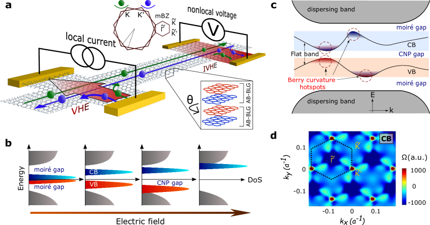
For detecting bulk valley current, we follow a measurement scheme similar to that used for detecting spin current in spintronics devices [30, 31], as shown in Fig. 1a. A finite charge current is passed using two local probes at two opposite sides of the device channel. VHE drives a valley current along the channel and a voltage, is generated in the nonlocal probes by inverse VHE. We quantify this as nonlocal resistance . We independently control both the charge density and the perpendicular electric displacement field aided by the dual-gated structure of our devices using a metal top gate and highly doped silicon back gate (see Methods).
The perpendicular electric field has a profound effect on the band structure of TDBG [8, 10, 11, 7, 9]. As depicted in Fig. 1b, at zero electric field, the system has low energy flat bands separated from higher energy dispersing bands by two moiré gaps. As the electric field is increased, a gap opens up at the CNP separating two flat bands. The moiré gaps close sequentially upon further increase of the electric field. In Fig. 1c we present a schematic of the band structure at finite electric field and show the existence of Berry curvature hotspots in the flat bands. The color scale plot of calculated Berry curvature in Fig. 1d depicts the locations of hotspots in the -space of the conduction band for valley. Details of band structure and Berry curvature map is provided in Supplementary Sec. I.
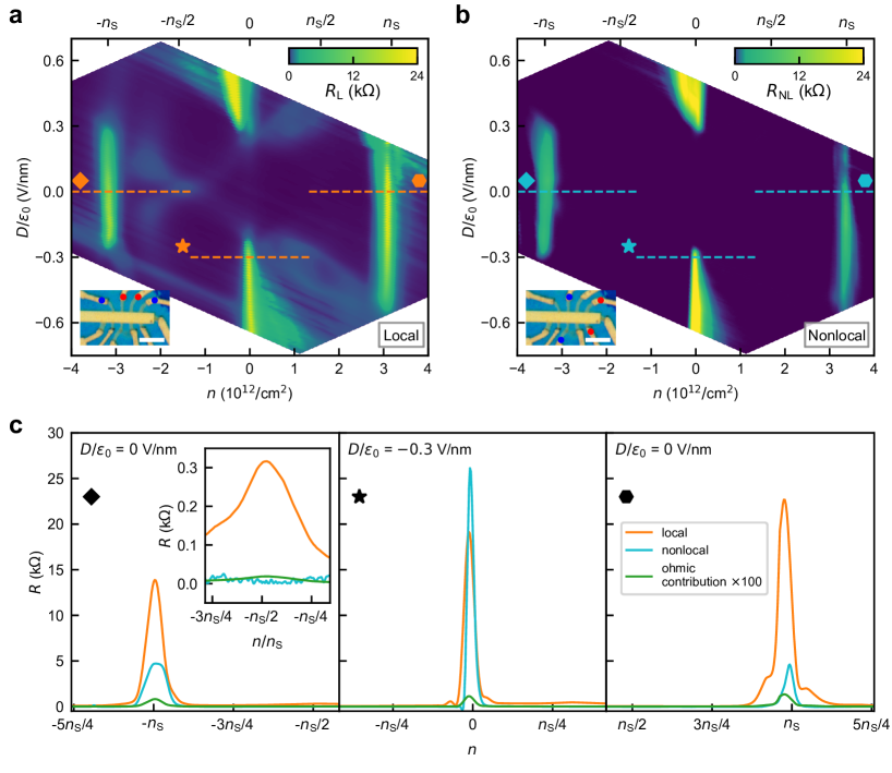
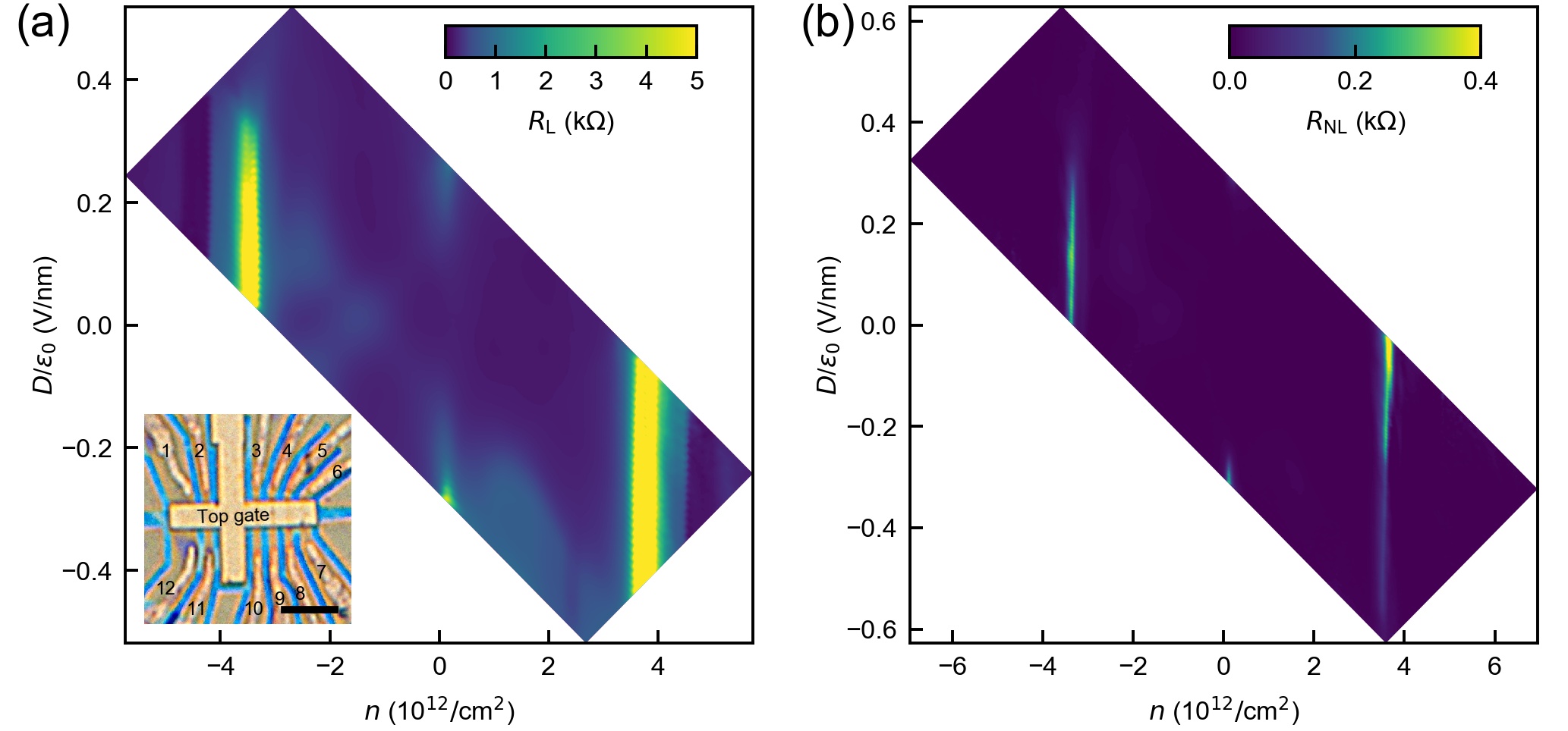
We now present the experimental results for a TDBG device with twist angle 1.18. This device shows a high degree of twist angle homogeneity over 8 microns; this is crucial for observing nonlocal resistance (Supplementary Sec. III). In Fig. 2a, we show a color scale plot of four-probe local resistance as a function of perpendicular electric field and charge density. We see large resistance at at high electric field due to gap opening at CNP, and at cm-2 corresponding to the moiré gaps. Here is the number of electrons required to fill one flat band. In Fig. 2b, we plot the measured nonlocal resistance which is large only at the gaps. Apart from the resistance peak at the gaps, there are other high resistance regions in the local resistance, characteristics to small-angle TDBG [8, 10, 11, 7, 9]. Such examples are the cross-like feature originating at in the hole side and the ring-like regions in the electron side for around 0.3 V/nm. The absence of these features in the nonlocal signal provides evidence that the nonlocal signal is distinct from the local resistance and is only appreciable when the Fermi energy crosses the gaps that possess large Berry curvature.
In Fig. 2c, we plot line slices from the color plots to show both the local and nonlocal resistances as a function of charge density. This clearly shows a large nonlocal signal at , corresponding to the moiré gaps at (left and right panels). In the middle panel, we plot the resistance at CNP for V/nm. On the same plot, we additionally plot the ohmic contribution to the nonlocal resistance due to stray current [32]. The calculated ohmic contribution (in Methods), being at least two orders of magnitude lower, cannot account for the large nonlocal resistance we observe.
Now we discuss an interesting difference in nonlocal resistance of TDBG compared to hBN aligned MLG [22] or gapped BLG [23, 24]. In a flat band system, the kinetic energy of the electrons is quenched. As the electrons slow down, with reduced Fermi velocity , they start to see an enhanced effect of the other energy scales in the system, for example, the - interaction. In a similar way, smaller renormalizes the gap. The enhancement of the effective band gap results in the spreading of the Berry curvature hotspots. To quantitatively understand this effect, we consider the Berry curvature of a gapped (2) MLG with renormalized to incorporate the effect of band flatness, . We find that the Berry curvature hotspot extends more in the -space as is decreased (Supplementary Sec. VIII). As a result, is appreciable over a large range of charge density around the gap in TDBG. This is evident in Fig. 2c as the nonlocal resistance peak is broad in the charge density axis. On the other hand, in the earlier reported systems [22, 23, 24] nonlocal resistance falls more rapidly than the local resistance, as the charge density is tuned away from the gaps (comparison in Supplementary Sec. IX).
We now proceed to understand the microscopic origin of the nonlocal signal. For diffusive transport of valley polarized electrons through the bulk, the nonlocal resistance generated via VHE is given by [22]:
| (1) |
Here, is the valley Hall conductivity, indicates the valley diffusion length, with and being the length and the width of the Hall bar channel, respectively. This equation holds good when , and results in a scaling relation between the local and the nonlocal resistance, with .
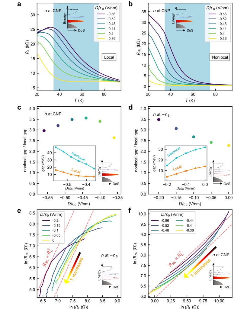
To examine the scaling relation we measure temperature dependence of the local and the nonlocal resistance for different , as plotted in Fig. 3a and Fig. 3b respectively, for the case of CNP. The local resistance shows Arrhenius activation behavior due to gaps in the system. The nonlocal resistance also follows activation behavior, but with higher gaps than the local resistance. In Fig. 3c and in Fig. 3d, we plot the ratio of the nonlocal to the local gap as a function of electric field for and , respectively. The insets of Fig. 3c and Fig. 3d show the values of the activation gaps as a function of electric field. Although the individual gaps are tuned by the electric field, the ratio varies within 2.3 to 3.5. The ratio being close to 3 establishes and hence supports bulk valley transport through equation (1). Also, this measurement reinforces our understanding that the contribution of in is minimal.
Now we closely examine the cubic scaling relation as a function of temperature (for scaling as a function of electric field, see Supplementary Sec. V). In Fig. 3e and Fig. 3f, we plot the nonlocal resistance against the local resistance in logarithmic scale with temperature as a parameter. Fig. 3e shows the case for , where the temperature varies from 10 K to 75 K. The scaling remains cubic, with deviation at low . This low temperature deviation from cubic scaling to being nearly independent of local resistance is consistent with the literature [23, 24]. At low temperature, the system enters into a large valley Hall angle regime, where the assumption is no longer valid [33].
The case where the system is at the charge neutrality is shown in Fig. 3f (the chosen range of temperature for showing scaling is shaded by blue in Fig. 3a and Fig. 3b). The scaling is cubic in intermediate temperature range, consistent with bulk valley transport, with departures at both ends. We note that in equation (1) can have temperature dependence and decrease from its quantized value at elevated temperatures compared to the gap [23]. Such a phenomenon can explain the departure from cubic scaling at the high temperature end. The low temperature deviation at CNP is different from that in the case of , as a transition to higher power laws occurs. We note that the nonlocal signal at CNP originates due to Berry curvature hotspots located at the edge of flat bands (See Supplementary Sec. I for at CNP in TDBG). At low temperatures, strong - correlations may give rise to edge states [34].
Twisted double bilayer graphene offers a unique platform since it provides electrical control over the flatness of bands through and the band gap it hosts. Our study shows that one can further use this electrical control to induce bulk valley current and offers new opportunities in valleytronics – via manipulating valley current by the tunable band gaps and the band flatness in twistronics. In particular, we show that the renormalized velocity in a flat band causes momentum spreading out of the Berry curvature hotspots. While we observe bulk valley current at elevated temperature, we cannot exclude the possibility that at low temperatures the nonlocal response is additionally mediated by the edge modes associated to the valley Hall effect or other spontaneous quantum Hall effect [34, 35] resulting from flat Chern bands [19]. The recent observation of anomalous Hall effect (AHE) and orbital magnetism in hBN-aligned TBG has been associated to the occupation of an excess valley- and spin-polarized Chern band by spontaneously breaking time-reversal symmetry [5, 6]. Our demonstration of VHE by nonlocal transport in TDBG, while preserving valley degeneracy, provides strong evidence that VHE state is indeed the parent state of the AHE state. We expect AHE state in TDBG as well, when the valley symmetry is broken. Additionally, our work opens up new possibilities to explore chargeless valley transport in other moiré systems like trilayer graphene aligned with hBN, twisted trilayer graphene and other twisted transition metal dichalcogenides having topological Chern bands.
Methods:
Our dual gated devices are made of hBN/TDBG/hBN stacks on SiO2( 280 nm)/Si++ substrate. To make the stacks, we exfoliate graphene and choose suitable bilayer graphene flakes based on optical contrast and then confirm the layer number by Raman spectroscopy. The suitable hBN flakes are selected based on color, and we confirm the thickness by AFM after the stack is completed. Bilayer graphene flakes are sliced into two halves using a tapered optical fiber scalpel, a method reported in [36]. Subsequently, the flakes are assembled using the standard poly(propylene) carbonate (PPC) based dry transfer method [37]. The twist angle is introduced by rotating the bottom stage during the pick up of the second half of the graphene. Subsequently, we define the geometry of the devices by e-beam lithography, followed by CHF3 + O2 plasma etching. One-dimensional edge contacts to the graphene are made by etching the stack and depositing Cr/Pd/Au. The top gate is made by depositing Cr/Au.
We fabricate and measure nonlocal transport in multiple devices. The dual-gated structure using a metal top gate and highly doped silicon back gate enables us to have independent control of both the charge density and the perpendicular electric displacement field given by and , where and are the capacitance per unit area of the top and the back gate respectively, and is the charge of an electron. All the data reported in the main manuscript are measured using Device 1 with twist angle 1.18. We present data from another device with twist angle 1.24 in Sec. VI of the Supplementary. The twist angle is calculated from where , nm is the lattice constant of graphene.
The transport measurements reported in the main text and the supplementary are conducted using a low frequency ( 17 Hz) lock-in technique by sending a current 10 nA and measuring the voltage after amplifying using SR560 preamplifier or preamplifier model 1021 by DL instruments, Ithaca. Additionally, we perform dc measurements to verify that the measured nonlocal signal is repeatable and independent of the measurement scheme (Supplementary Sec. II). We further checked that the nonlocal signal is consistent with reciprocity (Supplementary Sec. IV). The ohmic contribution to the nonlocal resistance due to stray current, as plotted in Fig. 2c, has been calculated by using the van der Pauw formula, [23]. Here, and are the length and width of the conduction channel, respectively. For the device presented in the main text, we choose =4 µm and =2 µm for performing the nonlocal measurements. This contribution decays exponentially along the length of the conduction channel. For the local measurements, we use the four-probe method and choose both and to be 2 µm from the same device, allowing us to use the relation in the main text.
References
- Kim et al. [2017] K. Kim, A. DaSilva, S. Huang, B. Fallahazad, S. Larentis, T. Taniguchi, K. Watanabe, B. J. LeRoy, A. H. MacDonald, and E. Tutuc, Tunable moiré bands and strong correlations in small-twist-angle bilayer graphene, Proceedings of the National Academy of Sciences 114, 3364 (2017).
- Cao et al. [2018a] Y. Cao, V. Fatemi, A. Demir, S. Fang, S. L. Tomarken, J. Y. Luo, J. D. Sanchez-Yamagishi, K. Watanabe, T. Taniguchi, E. Kaxiras, R. C. Ashoori, and P. Jarillo-Herrero, Correlated insulator behaviour at half-filling in magic-angle graphene superlattices, Nature 556, 80 (2018a).
- Cao et al. [2018b] Y. Cao, V. Fatemi, S. Fang, K. Watanabe, T. Taniguchi, E. Kaxiras, and P. Jarillo-Herrero, Unconventional superconductivity in magic-angle graphene superlattices, Nature 556, 43 (2018b).
- Lu et al. [2019] X. Lu, P. Stepanov, W. Yang, M. Xie, M. A. Aamir, I. Das, C. Urgell, K. Watanabe, T. Taniguchi, G. Zhang, A. Bachtold, A. H. MacDonald, and D. K. Efetov, Superconductors, orbital magnets and correlated states in magic-angle bilayer graphene, Nature 574, 653 (2019).
- Sharpe et al. [2019] A. L. Sharpe, E. J. Fox, A. W. Barnard, J. Finney, K. Watanabe, T. Taniguchi, M. A. Kastner, and D. Goldhaber-Gordon, Emergent ferromagnetism near three-quarters filling in twisted bilayer graphene, Science 365, 605 (2019).
- Serlin et al. [2020] M. Serlin, C. L. Tschirhart, H. Polshyn, Y. Zhang, J. Zhu, K. Watanabe, T. Taniguchi, L. Balents, and A. F. Young, Intrinsic quantized anomalous Hall effect in a moiré heterostructure, Science 367, 900 (2020).
- Burg et al. [2019] G. W. Burg, J. Zhu, T. Taniguchi, K. Watanabe, A. H. MacDonald, and E. Tutuc, Correlated Insulating States in Twisted Double Bilayer Graphene, Physical Review Letters 123, 197702 (2019).
- Shen et al. [2020] C. Shen, Y. Chu, Q. Wu, N. Li, S. Wang, Y. Zhao, J. Tang, J. Liu, J. Tian, K. Watanabe, T. Taniguchi, R. Yang, Z. Y. Meng, D. Shi, O. V. Yazyev, and G. Zhang, Correlated states in twisted double bilayer graphene, Nature Physics 10.1038/s41567-020-0825-9 (2020).
- Adak et al. [2020] P. C. Adak, S. Sinha, U. Ghorai, L. D. V. Sangani, K. Watanabe, T. Taniguchi, R. Sensarma, and M. M. Deshmukh, Tunable bandwidths and gaps in twisted double bilayer graphene on the verge of correlations, Phys. Rev. B 101, 125428 (2020).
- Liu et al. [2019a] X. Liu, Z. Hao, E. Khalaf, J. Y. Lee, K. Watanabe, T. Taniguchi, A. Vishwanath, and P. Kim, Spin-polarized Correlated Insulator and Superconductor in Twisted Double Bilayer Graphene, arXiv:1903.08130 [cond-mat] (2019a), arXiv:1903.08130 [cond-mat] .
- Cao et al. [2019] Y. Cao, D. Rodan-Legrain, O. Rubies-Bigorda, J. M. Park, K. Watanabe, T. Taniguchi, and P. Jarillo-Herrero, Electric Field Tunable Correlated States and Magnetic Phase Transitions in Twisted Bilayer-Bilayer Graphene, arXiv:1903.08596 [cond-mat] (2019), arXiv:1903.08596 [cond-mat] .
- Chen et al. [2019a] G. Chen, L. Jiang, S. Wu, B. Lyu, H. Li, B. L. Chittari, K. Watanabe, T. Taniguchi, Z. Shi, J. Jung, Y. Zhang, and F. Wang, Evidence of a gate-tunable Mott insulator in a trilayer graphene moiré superlattice, Nature Physics 15, 237 (2019a).
- Chen et al. [2019b] G. Chen, A. L. Sharpe, P. Gallagher, I. T. Rosen, E. J. Fox, L. Jiang, B. Lyu, H. Li, K. Watanabe, T. Taniguchi, J. Jung, Z. Shi, D. Goldhaber-Gordon, Y. Zhang, and F. Wang, Signatures of tunable superconductivity in a trilayer graphene moiré superlattice, Nature 572, 215 (2019b).
- Chen et al. [2020] G. Chen, A. L. Sharpe, E. J. Fox, Y.-H. Zhang, S. Wang, L. Jiang, B. Lyu, H. Li, K. Watanabe, T. Taniguchi, Z. Shi, T. Senthil, D. Goldhaber-Gordon, Y. Zhang, and F. Wang, Tunable correlated Chern insulator and ferromagnetism in a moiré superlattice, Nature 579, 56 (2020).
- Suárez Morell et al. [2010] E. Suárez Morell, J. D. Correa, P. Vargas, M. Pacheco, and Z. Barticevic, Flat bands in slightly twisted bilayer graphene: Tight-binding calculations, Physical Review B 82, 121407 (2010).
- Lopes dos Santos et al. [2012] J. M. B. Lopes dos Santos, N. M. R. Peres, and A. H. Castro Neto, Continuum model of the twisted graphene bilayer, Physical Review B 86, 155449 (2012).
- Bistritzer and MacDonald [2011] R. Bistritzer and A. H. MacDonald, Moiré bands in twisted double-layer graphene, Proceedings of the National Academy of Sciences 108, 12233 (2011).
- Song et al. [2015] J. C. W. Song, P. Samutpraphoot, and L. S. Levitov, Topological Bloch bands in graphene superlattices, Proceedings of the National Academy of Sciences 112, 10879 (2015).
- Zhang et al. [2019] Y.-H. Zhang, D. Mao, Y. Cao, P. Jarillo-Herrero, and T. Senthil, Nearly flat Chern bands in moir\’e superlattices, Physical Review B 99, 075127 (2019).
- Xiao et al. [2010] D. Xiao, M.-C. Chang, and Q. Niu, Berry phase effects on electronic properties, Reviews of Modern Physics 82, 1959 (2010).
- Nagaosa et al. [2010] N. Nagaosa, J. Sinova, S. Onoda, A. H. MacDonald, and N. P. Ong, Anomalous Hall effect, Reviews of Modern Physics 82, 1539 (2010).
- Gorbachev et al. [2014] R. V. Gorbachev, J. C. W. Song, G. L. Yu, A. V. Kretinin, F. Withers, Y. Cao, A. Mishchenko, I. V. Grigorieva, K. S. Novoselov, L. S. Levitov, and A. K. Geim, Detecting topological currents in graphene superlattices, Science 346, 448 (2014).
- Shimazaki et al. [2015] Y. Shimazaki, M. Yamamoto, I. V. Borzenets, K. Watanabe, T. Taniguchi, and S. Tarucha, Generation and detection of pure valley current by electrically induced Berry curvature in bilayer graphene, Nature Physics 11, 1032 (2015).
- Sui et al. [2015] M. Sui, G. Chen, L. Ma, W.-Y. Shan, D. Tian, K. Watanabe, T. Taniguchi, X. Jin, W. Yao, D. Xiao, and Y. Zhang, Gate-tunable topological valley transport in bilayer graphene, Nature Physics 11, 1027 (2015).
- Chebrolu et al. [2019] N. R. Chebrolu, B. L. Chittari, and J. Jung, Flat bands in twisted double bilayer graphene, Physical Review B 99, 10.1103/PhysRevB.99.235417 (2019).
- Koshino [2019] M. Koshino, Band structure and topological properties of twisted double bilayer graphene, Physical Review B 99, 235406 (2019).
- Lee et al. [2019] J. Y. Lee, E. Khalaf, S. Liu, X. Liu, Z. Hao, P. Kim, and A. Vishwanath, Theory of correlated insulating behaviour and spin-triplet superconductivity in twisted double bilayer graphene, Nature Communications 10, 5333 (2019).
- Choi and Choi [2019] Y. W. Choi and H. J. Choi, Intrinsic band gap and electrically tunable flat bands in twisted double bilayer graphene, Physical Review B 100, 10.1103/PhysRevB.100.201402 (2019).
- Liu et al. [2019b] J. Liu, Z. Ma, J. Gao, and X. Dai, Quantum Valley Hall Effect, Orbital Magnetism, and Anomalous Hall Effect in Twisted Multilayer Graphene Systems, Physical Review X 9, 031021 (2019b).
- Valenzuela and Tinkham [2006] S. O. Valenzuela and M. Tinkham, Direct electronic measurement of the spin Hall effect, Nature 442, 176 (2006).
- Abanin et al. [2009] D. A. Abanin, A. V. Shytov, L. S. Levitov, and B. I. Halperin, Nonlocal charge transport mediated by spin diffusion in the spin Hall effect regime, Physical Review B 79, 035304 (2009).
- Abanin et al. [2011] D. A. Abanin, S. V. Morozov, L. A. Ponomarenko, R. V. Gorbachev, A. S. Mayorov, M. I. Katsnelson, K. Watanabe, T. Taniguchi, K. S. Novoselov, L. S. Levitov, and A. K. Geim, Giant Nonlocality Near the Dirac Point in Graphene, Science 332, 328 (2011).
- Beconcini et al. [2016] M. Beconcini, F. Taddei, and M. Polini, Nonlocal topological valley transport at large valley Hall angles, Physical Review B 94, 121408 (2016).
- Zhang et al. [2011] F. Zhang, J. Jung, G. A. Fiete, Q. Niu, and A. H. MacDonald, Spontaneous Quantum Hall States in Chirally Stacked Few-Layer Graphene Systems, Physical Review Letters 106, 156801 (2011).
- Jung et al. [2011] J. Jung, F. Zhang, and A. H. MacDonald, Lattice theory of pseudospin ferromagnetism in bilayer graphene: Competing interaction-induced quantum Hall states, Physical Review B 83, 115408 (2011).
- Sangani et al. [2020] L. D. V. Sangani, S. K. R.S, P. C. Adak, S. Sinha, A. H. Marchawala, T. Taniguchi, K. Watanabe, and M. Deshmukh, Facile deterministic cutting of 2D materials for twistronics using a tapered fibre scalpel., Nanotechnology 10.1088/1361-6528/ab8b93 (2020).
- Wang et al. [2013] L. Wang, I. Meric, P. Y. Huang, Q. Gao, Y. Gao, H. Tran, T. Taniguchi, K. Watanabe, L. M. Campos, D. A. Muller, J. Guo, P. Kim, J. Hone, K. L. Shepard, and C. R. Dean, One-Dimensional Electrical Contact to a Two-Dimensional Material, Science 342, 614 (2013).
Acknowledgements:
We thank Allan MacDonald, Justin Song, Rajdeep Sensarma, Vibhor Singh, Sajal Dhara and Biswajit Datta for helpful discussions and comments. We acknowledge Nanomission grant SR/NM/NS-45/2016 and Department of Atomic Energy of Government of India for support. Preparation of hBN single crystals is supported by the Elemental Strategy Initiative conducted by the MEXT, Japan and JSPS KAKENHI Grant Number JP15K21722. This work is supported by the Korean NRF for B.L.C. through Basic Science Research Program of the National Research Foundation of Korea (NRF) funded by the Ministry of Education Grant No. 2018R1A6A1A06024977 and Grant No. NRF-2020R1A2C3009142, and for J.J. through Samsung Science and Technology Foundation under project no. SSTF-BA1802-06.
Author contributions:
P.C.A, S.S, R.S.S.K., and L.D.V.S. fabricated the devices. P.C.A. and S.S. did the measurements and analyzed the data. B.L.C. and J.J. did the theoretical calculation. K.W. and T.T. grew the hBN crystals. P.C.A, S.S., and M.M.D. wrote the manuscript with inputs from everyone. M.M.D. supervised the project.
Supplementary Information
I Calculation of band structure and valley Hall conductivity in TDBG
As discussed in the theory paper Ref. [1], moiré bands theory for the moiré pattern superlattice [2] and the accurate continuum models [3] are used to obtain the electronic structure of the twisted double bilayer graphene (TDBG). The continuum model of Bistritzer-MacDonald for the twisted bilayer graphene (TBG) [2] is extended to the case of twisted double bilayer graphene (TDBG), the Hamiltonian of TDBG at the valley K with the interlayer coupling between the twisted layers through a first-harmonic stacking-dependent interlayer tunneling function, and subject to intralayer potentials as
| (S1) |
where such that the relative twist angle between the bilayers is .
The Dirac Hamiltonian given by includes a phase shift due to a rotation such that , where and are the graphene sublattice pseudospin Pauli matrices, and the momentum is defined in the xy plane , where we assume K valley unless stated otherwise. The Fermi velocity defined from is related to the intralayer nearest-neighbor hopping term t0 = -3.1 eV that captures the experimental moiré band features better [4].
The top and bottom bilayer graphene (BG) are labeled through the positive/negative (+/-) rotation signs, while in turn we have top/bottom (t/b) graphene layers within each BG that are coupled through the matrices . The interlayer coupling model of a bilayer graphene is given by
| (S2) |
satisfying for AB or BA () stacking-dependent interlayer coupling that consists of a minimal coupling term plus remote hopping contributions through the terms t3 = 0.283, t4 = 0.138 eV, giving rise to trigonal warping and electron-hole asymmetry. The operators include the phases due to layer rotation. The Hamiltonian of graphene is given by where the second term adds a 0.015 eV sublattice potential at the higher energy dimer sites at the t/b layers [5], that depends on AB or BA stacking , respectively. The site potentials are mapped on its sublattices through where = 1, 2, 3, 4 are the layer labels from top to bottom, and is a identity matrix. Here, we have an additional control knob to change the electronic structure through a perpendicular external electric field that modifies the interlayer potential values in equation (S1). The potential drops introduced by an external electric field could be modeled through the parameter set , , redefined as and , where is the interlayer potential difference between each BG.
We can identify the interlayer tunneling with the first harmonic expansion coefficient of the interlayer coupling such that [3, 5], and for simplicity we use the same AB stacking tunneling within each Bernal BG and the twisted interfaces. In the small-angle approximation, the interlayer coupling Hamiltonian is given by
| (S3) |
where the three vectors and are proportional to twist angle and is the Brillouin zone corner length of graphene, whose lattice constant is , and here the indices label the sublattices of neighboring twisted surface layers. The interlayer coupling matrices between the two rotated adjacent layers are given by
| (S4) |
using a form that distinguishes interlayer tunneling matrix elements and for different and same sublattice sites between the layers. The convention taken here for the matrices [3] assumes an initial AA stacking configuration and differs by a phase factor with respect to the initial AB stacking [6, 7]. The greater interlayer separation compared to the carbon-carbon distances lead to slowly varying interlayer tunneling function and the moiré patterns can often be accurately described within a first-harmonic approximation [2, 3]. Furthermore, the effects of atomic relaxation in the moiré patterns lead to corrugations that have non-negligible effects in the details of the electronic structure for both intralayer potentials and interlayer coupling [8]. In the case of , we proposed a single parameter relation through , where , , as discussed in Ref. [1] (in its Supplementary information). Our calculations have used a configuration space with variable cutoff in momentum space of a radius of up to using Hamiltonian matrices with sizes as large as such that to obtain converged results in the limit of small and large .
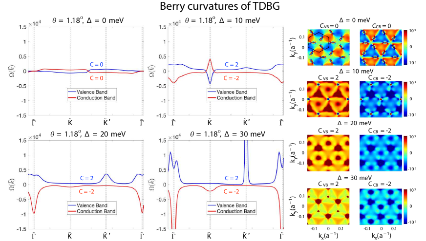
The possibility of band gap opening at charge neutrality point (CNP), primary gap (), through an electric field together with the presence of moiré gaps (secondary gaps, ) with the higher-energy bands leads to well-defined valley Chern numbers. The valley Chern numbers were calculated through
| (S5) |
by integrating the moiré Brillouin zone for each valley the Berry curvature for the -th band through [9]
| (S6) |
where for every k point we take sums through all the neighboring bands, the are the moiré superlattice Bloch states, and are the eigenvalues.
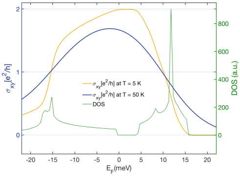
The Hall conductivity that results due to a nonzero Berry curvature () at a particular valley of graphene (K or K′) is given by [10]
| (S7) |
where indicates the bank index and denotes the Fermi occupation function. At low temperature (shown in orange curve for 5 K in Fig. S3), it saturates to in the band gap between the flat bands. Away from the gap, it starts decreasing since the Berry curvature in the low energy conduction band and valence band have opposite signs, as seen from the line plots in Fig. S2. This decrease of away from the CNP gap in TDBG is asymmetric in nature, which is in contrary to that obtained for bilayer graphene [11, 12]. The Hall conductivity is also shown for an elevated temperature of 50 K (blue curve) where we have observed bulk valley transport at the CNP gap. The decrease in from its low temperature value of at the gap is due to the thermal excitation of valence band electrons to the conduction band. The valley Hall conductivity, , is obtained by adding the contribution to the Hall conductivity from the individual valleys at K and K′, and is given by [11].
II Nonlocal transport measurement
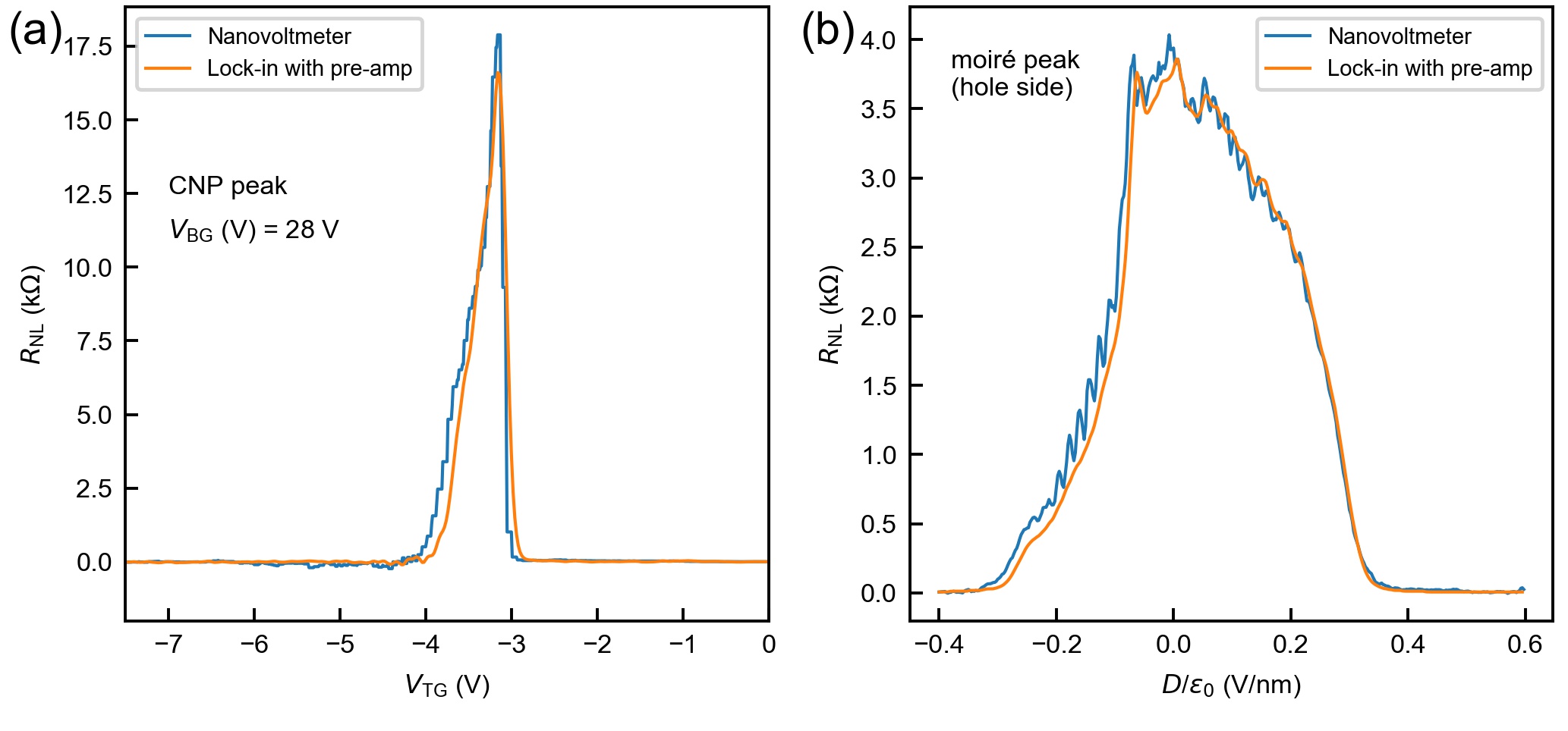
The transport measurement reported in the main text and all other sections in the supplementary was measured using a low frequency ( 17 Hz) lock-in technique by sending a current 10 nA and measuring the voltage after amplifying using SR560 preamplifier or preamplifier model 1021 by DL instruments, Ithaca. Since the nonlocal resistance is appreciable when the system is gapped, spurious signal can be measured for these high resistivity states [13, 11]. To verify the nonlocal resistance we measured is not a measurement artifact, we employ Keithley 2182 nanovoltmeter to measure dc voltage while sending current using Keithley 6221 current source. The nanovoltmeter has input impedance > 10 G while the SR560 or DL 1021 preamplifier has an input impedance of 100 M. In Fig. S4(a) we have plotted the nonlocal resistance as a function of top gate voltage around the CNP at V measured both by the lock-in method aided by the preamplifier and the dc measurement using nanovoltmeter. For measurement using the nanovoltmeter, we measured resistance both in forward and reverse directions and took the average resistance to nullify any dc voltage drop due to thermo-electric effect at various junctions of the current path inside the cryostat. In Fig. S4(b) we plotted the nonlocal resistance of the moiré peak at the hole side as a function of the perpendicular electric field using the two schemes. As seen from both Figs. S4(a) and S4(b), the resistance values are independent of the measurement schemes. All the measurements subsequently were done using lock-in with the preamplifier.
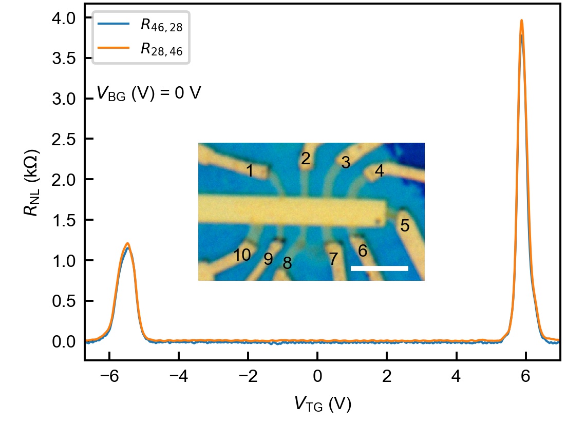
III Angle homogeneity for nonlocal detection of valley current
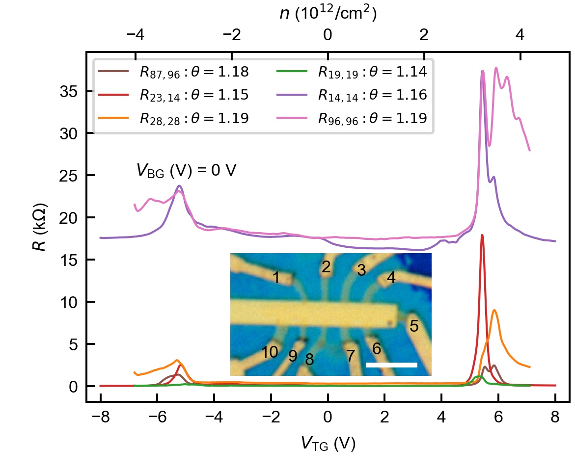
The twist angle homogeneity is an important prerequisite for measuring nonlocal valley transport in twisted graphene devices. This is because the generation of valley current in the injection probes happens when the Fermi energy lies in a Berry curvature hotspot, i.e., the Fermi energy lies near a gap. This requires the charge density to be tuned by the gates to specific values: (CNP gap) or (moiré gap), where with nm being the lattice constant of graphene. Now for detecting the valley current, the detection probes have the same requirement. Since depends on , the local twist angle should be the same in both the pairs of injection and detection probes as well as the valley current path.
To estimate the local twist angle near various probes we measure two-probe and four-probe resistance using different combinations of current and voltage probes. In Fig. S5 we present such different plots of local resistance as a function of for V. All the curves have two moiré peaks corresponding to . The difference in the positions of the two peaks on the -axis corresponds to , which is used to estimate the local twist angle. We find that the twist angle to vary between 1.14 to 1.19, establishing that the device has good angle homogeneity.
IV Reciprocity of the nonlocal resistance measurement
For the Onsager reciprocal relations to be valid, the nonlocal resistance we measure should be the same if one swaps the injection and the detection terminals [11]. We verify this in Fig. S6 where we present nonlocal resistance as a function of with V for two reciprocal combinations of injection and detection probes. We find that the nonlocal resistance does not change if we swap the terminals.
V Additional data on scaling
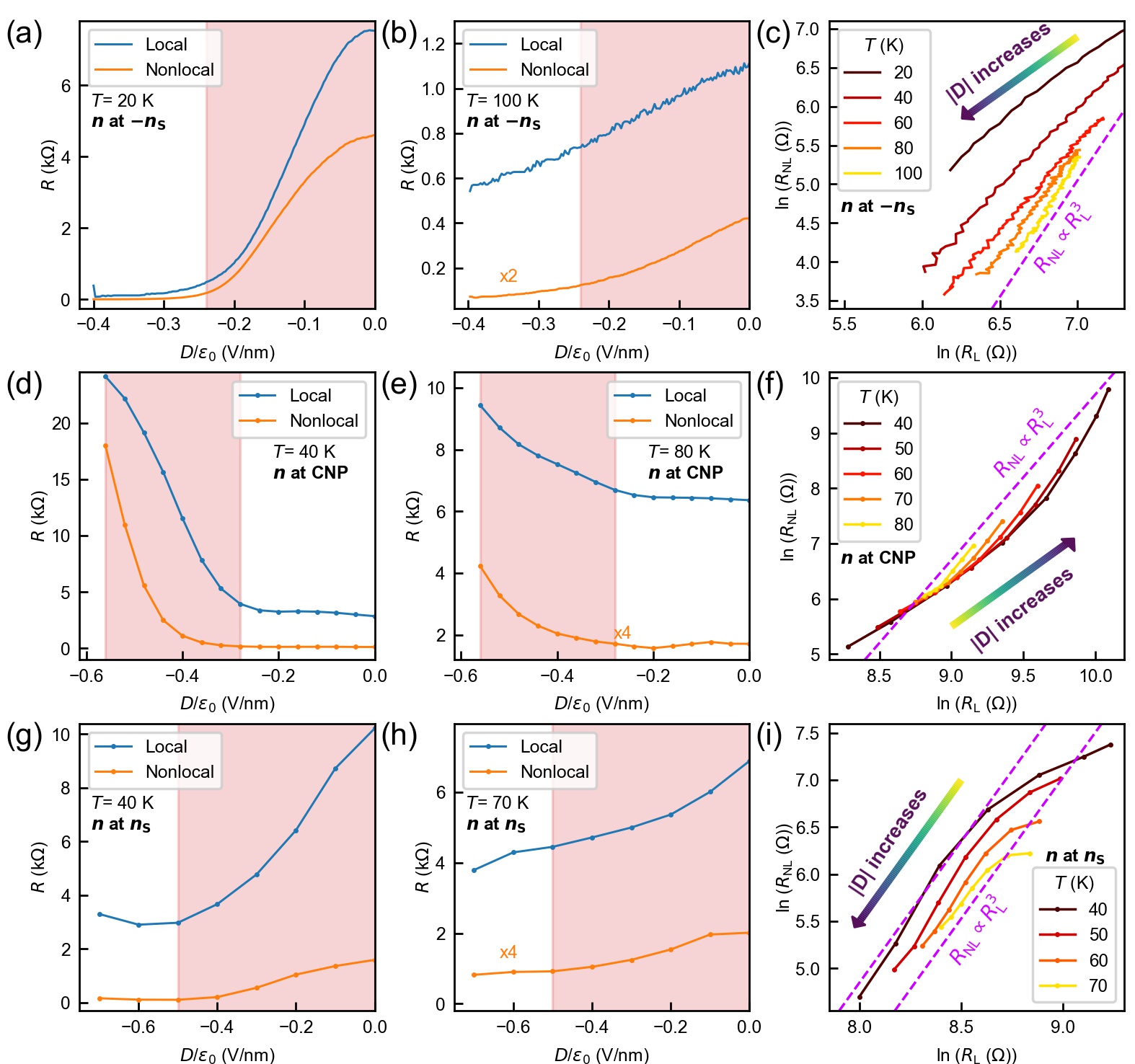
A tell-tale signature of bulk valley current is cubic scaling between the nonlocal and local resistances. In Fig. 3e and Fig. 3f of the main text, we had demonstrated the cubic scaling by taking temperature as a parameter for some fixed electric fields. In Fig. S7, we show the cubic scaling at different fixed temperatures for the CNP (Fig. S7(f)) and moiré gaps (Fig. S7(c) for and Fig. S7(i) for ) by taking the electric field () as a parameter. For in Fig. S7(c), we see cubic scaling towards the high temperature end. The case for in Fig. S7(i) shows cubic scaling in the high electric field end, while the scaling deviates from cubic and saturates towards the low electric field end where the band gap at is higher [14]. This saturation at high band gap regime is attributed to large valley Hall angle physics [15] and is also seen in earlier studies at the CNP gap of bilayer graphene [11]. In Fig. S7(f) we find that the CNP shows cubic scaling at high temperatures. As the temperature is lowered (brown and black curve in Fig. S7(f)), the scaling deviates from cubic to higher exponents in the high electric field end. This is similar to that in Fig. 3(f) of the main text, where high and low shows the same departure.
VI Data from the second device
In Fig S8, we present local and nonlocal resistance from the Device 2 which has a twist angle of .
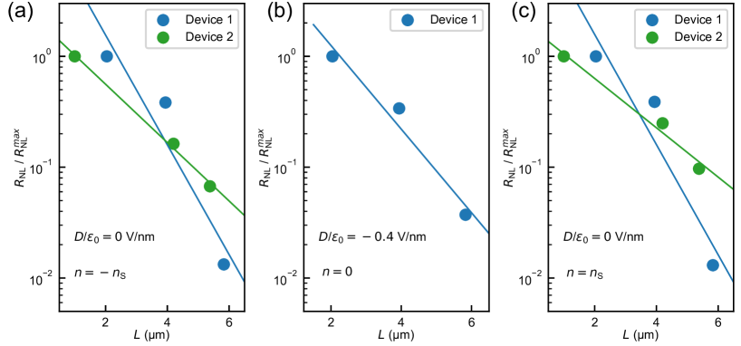
VII Decay of Nonlocal resistance with length
The dependence of the nonlocal resistance on the length of the current path is governed by the valley diffusion length , as seen from equation (S8),
| (S8) |
Here, is the valley Hall conductivity. and represent the length and width of the Hall bar channel, respectively. To extract we plot the decay of the nonlocal signal along the sample length at the moiré gaps and the CNP in Fig. S9. We fit the exponential decay using equation (S8) and extract out for both the devices. The data for Device 1 is plotted at 35 K to negate low temperature effects. For moiré gaps, we find to be 0.9 µm and 1.8 µm for Device 1 and Device 2 respectively. At the CNP, is 1.15 µm for Device 1. These values are similar to those obtained in bilayer graphene [11].
VIII Effect of band flatness on Berry curvature hotspot
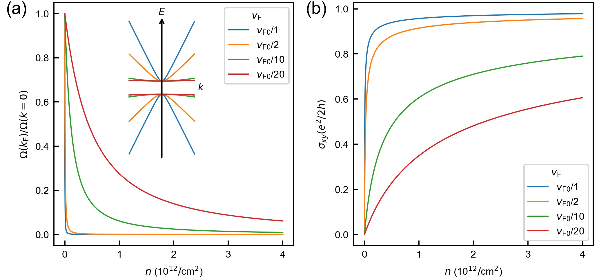
To understand the effect of a flat band on the Berry curvature hotspot, we consider a simple band structure of gapped monolayer graphene. We choose the monolayer graphene Hamiltonian since, for a flat band, in any twisted system, there is no reason in general for the linear term in momentum to be zero. The Hamiltonian for the gapped monolayer graphene is given by, . Here is the band gap between two energy bands given by . We incorporate the band flatness by renormalizing the term in the Hamiltonian, whereas in the case of monolayer graphene m/s . The Berry curvature is given by . With the charge density given by and , the Berry curvature at the Fermi wave vector is given by . In Fig. S10(a) we plot the Berry curvature as a function of charge density for monolayer graphene with a gap of meV and for different values of the renormalized velocity, . As is smaller, i.e., the band is flatter, we find that the Berry curvature is more delocalized away from the gap. In Fig. S10(b) we plot the contribution of the conduction band to the valley Hall conductivity given by, . We again find that in the case of flat band the Hall conductivity saturates to its asymptotic value much slower. The Berry curvature delocalization and slow saturation of Hall conductivity in flat band systems, as represented in Fig. S10, can be reproduced even by starting with a gapped bilayer graphene Hamiltonian.
IX Comparison of extent of nonlocal resistance peak with a system without flat bands
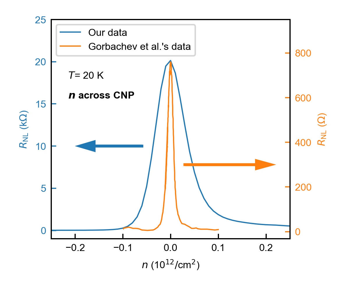
Here we compare the extent of the nonlocal signal in the charge density axis from our TDBG device with that of hBN aligned graphene device from Gorbachev et al. [16]. We compare the charge neutrality peak at = 20 K for both the devices. Upon application of a perpendicular electric field (shown for V/nm in Fig. S11), a gap opens up at charge neutrality within the flat bands in the TDBG device [14]. These bands have Berry curvature hotspots, as shown in Fig. S2. For the case of hBN aligned graphene, the superlattice potential results in opening up a gap between the valence band and conduction band at the charge neutrality [17]. This, too, results in Berry curvature hotspots at the band edges near the gap opening. However, unlike the case in small-angle TDBG, the resulting low energy bands are not flat. The broader extent of the nonlocal resistance in our data (the FWHM being 5 times larger) can be attributed to the spreading of Berry curvature hotspot due to flat bands in the TDBG system.
References
- Chebrolu et al. [2019] N. R. Chebrolu, B. L. Chittari, and J. Jung, Phys. Rev. B 99, 235417 (2019).
- Bistritzer and MacDonald [2011] R. Bistritzer and A. H. MacDonald, Proceedings of the National Academy of Sciences 108, 12233 (2011).
- Jung et al. [2014] J. Jung, A. Raoux, Z. Qiao, and A. H. MacDonald, Phys. Rev. B 89, 205414 (2014).
- Wong et al. [2015] D. Wong, Y. Wang, J. Jung, S. Pezzini, A. M. DaSilva, H.-Z. Tsai, H. S. Jung, R. Khajeh, Y. Kim, J. Lee, S. Kahn, S. Tollabimazraehno, H. Rasool, K. Watanabe, T. Taniguchi, A. Zettl, S. Adam, A. H. MacDonald, and M. F. Crommie, Phys. Rev. B 92, 155409 (2015).
- Jung and MacDonald [2014] J. Jung and A. H. MacDonald, Phys. Rev. B 89, 035405 (2014).
- Javvaji et al. [2020] S. Javvaji, J.-H. Sun, and J. Jung, Phys. Rev. B 101, 125411 (2020).
- Leconte et al. [2017] N. Leconte, J. Jung, S. Lebègue, and T. Gould, Phys. Rev. B 96, 195431 (2017).
- Jung et al. [2015] J. Jung, A. M. DaSilva, A. H. MacDonald, and S. Adam, Nature Communications 6, 6308 (2015).
- Xiao et al. [2010] D. Xiao, M.-C. Chang, and Q. Niu, Rev. Mod. Phys. 82, 1959 (2010).
- Lado and Fernández-Rossier [2015] J. L. Lado and J. Fernández-Rossier, Physical Review B 92, 115433 (2015).
- Shimazaki et al. [2015] Y. Shimazaki, M. Yamamoto, I. V. Borzenets, K. Watanabe, T. Taniguchi, and S. Tarucha, Nature Physics 11, 1032 (2015).
- Koshino [2009] M. Koshino, New Journal of Physics 11, 095010 (2009).
- Sui et al. [2015] M. Sui, G. Chen, L. Ma, W.-Y. Shan, D. Tian, K. Watanabe, T. Taniguchi, X. Jin, W. Yao, D. Xiao, and Y. Zhang, Nature Physics 11, 1027 (2015).
- Adak et al. [2020] P. C. Adak, S. Sinha, U. Ghorai, L. D. V. Sangani, K. Watanabe, T. Taniguchi, R. Sensarma, and M. M. Deshmukh, Phys. Rev. B 101, 125428 (2020).
- Beconcini et al. [2016] M. Beconcini, F. Taddei, and M. Polini, Phys. Rev. B 94, 121408 (2016).
- Gorbachev et al. [2014] R. V. Gorbachev, J. C. W. Song, G. L. Yu, A. V. Kretinin, F. Withers, Y. Cao, A. Mishchenko, I. V. Grigorieva, K. S. Novoselov, L. S. Levitov, and A. K. Geim, Science 346, 448 (2014).
- Song et al. [2015] J. C. W. Song, P. Samutpraphoot, and L. S. Levitov, Proceedings of the National Academy of Sciences 112, 10879 (2015).