Dipolar and magnetic properties of strongly absorbing hybrid interlayer excitons in pristine bilayer MoS2
Abstract
Van der Waals heterostructures composed of transition metal dichalcogenide monolayers (TMDs) are characterized by their truly rich excitonic properties which are determined by their structural, geometric and electronic properties: In contrast to pure monolayers, electrons and holes can be hosted in different materials, resulting in highly tunable dipolar manyparticle complexes. However, for genuine spatially indirect excitons, the dipolar nature is usually accompanied by a notable quenching of the exciton oscillator strength. Via electric and magnetic field dependent measurements, we demonstrate, that a slightly biased pristine bilayer MoS2 hosts strongly dipolar excitons, which preserve a strong oscillator strength. We scrutinize their giant dipole moment, and shed further light on their orbital- and valley physics via bias-dependent magnetic field measurements.
Introduction
The interest in excitons hosted in atomically thin materials was initially sparked by their giant oscillator strength and large binding energies, resulting from the canonical interplay of reduced dielectric screening and confinement of charge carriers in an atomically thin sheet wang2018 . The spectacular finding of extreme optical activity triggered a plethora of experiments, analyzing their chirality schaibley2016valleytronics , their magnetic behavior gong2013magnetoelectric ; srivastava2015valley ; stier2016exciton ; aivazian2015magnetic ; robert2020measurement , interactions yielding higher order multi-particle complexes Chernikov2014 and finally driving the field of opto-electronic applications wang2012electronics . In the latter, in particular the coupling to confined microcavity modes became a field of particular interest, giving rise to pronounced polaritonic phenomena up to ambient conditions lundt2016room ; liu2015strong ; schneider2018two . More recently, the sheet nature of TMDCs, which allows almost arbitrary stacking and alignment of multiple monolayers was harnessed to compose more complex electronic structures. One recurrent scheme in devices based on such van der Waals heterostructures are charge transfer phenomena, which yield the formation of dipolar excitons with electrons and holes confined in different layers rivera2015observation . While such excitons do have appealing properties, including enhanced nonlinearities borrowed from their dipolar character, the giant oscillator strength, which initially sparked the success of TMD excitons is strongly compromised by the reduced spatial overlap of electron and holes in separate layers. However, recently it was suggested that the hybridization of hole states in a pristine bilayer of MoS2 enables the formation of dipolar excitons, which combine a permanent dipole moment with a giant oscillator strength gerber2019interlayer . Here, we give evidence for this new species of TMD exciton: The dipolar character is clearly evidenced in field-dependent absorption measurements, while maintaining a substantial optical absorption. We further scrutinize the orbital- and valley composition by assessing the excitonic g-factor in the presence of a static electric field, and develop a consistent microscopic theory describing our main findings.
Experimental results
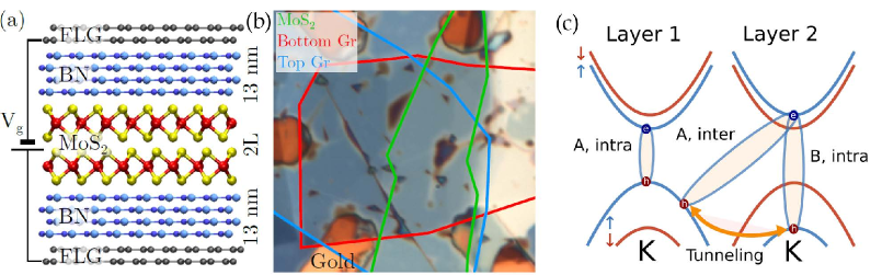
In order to characterize interlayer excitons with strong dipole moment in pristine MoS2 TMD bilayers, we fabricate a van der Waals heterostructure composed of few layer graphene (FLG), an approx. 13 nm thick layer of hexagonal boron nitride (BN), a pristine bilayer MoS2, another 13 nm thick BN and FLG (Fig. 1 a). Both FLG are electrically contacted to achieve a top and backgate which allows us to apply an out of plane electric field. A microscope image of the fully assembled device is shown in Fig. 1 b). The excitonic optical response of bilayer MoS2 is composed by the so-called A- and B- exciton transitions at the K and K’ point, respectively. As opposed to a monolayer, charge transfer processes further allow for the emergence of spatially indirect excitonic complexes in bilayers, which enriches the optical response. As schematically captured in Fig. 1 c) and anticipated in gerber2019interlayer , a hybrid resonance evolves by hybridizing an A-type interlayer transition with a B-type intralayer resonance. Such a hybrid transition consequently admixes the dipolar properties of interlayer excitons with the strong oscillator strength of TMDC intralayer resonances.
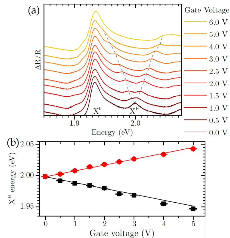
We first probe the optical response of our device via white light reflection spectroscopy at cryogenic temperatures (4 K), and plot the differential reflectivity normalized with respect to a reference spectrum recorded next to the structure. At zero gate voltage, we retrieve the characteristic absorption spectrum of bilayer MoS2, which is composed of two significant optical resonances in the energy range between 1.8 and 2.1 eV. These two absorption peaks have been assigned to the neutral A exciton transition at 1.95 eV, as well as the hybrid excitonic state which mixes A-inter- and B-intralayer states (see (Fig. 1 c) (denoted as XH in the following). We point out, that this hybrid mode displays a significant reflection signal, caused by a strong oscillator strength which is only smaller by approx. a factor of 4 as compared to the intralayer A-exciton.
Evident from the bias dependent reflectivity measurements in Fig. 2 a), the applied static electric field couples to out of plane dipoles via the Stark effect, modifying the exciton energy as with the out of plane electric dipole and the electric field. Since the XH dipole is not polarized in our white light reflection experiment, both dipole (pointing from layer 1 to layer 2 and vice versa) coexist at the same energy at zero electric field. The out of plane electrical field lifts this degeneracy ending up with two different absorption lines in the spectrum (Fig. 2 a). We note, that the application of only 5 V to our device yields a giant dipolar splitting of 100 meV of the two modes, which is only accompanied by a modest quenching of the oscillator strength.
For a quantitative analysis, we estimate the electric field from the gate voltage and the device geometry via a plate capacitor model (, laturia2018dielectric , following the approach discussed in wang2018electrical (see supplementary notes). We extracted the emission energy of both XH upper and lower branch which scales linearly with the gate voltage. By fitting our data, we directly yield a giant dipole moment of 0.48 nm for XH, which is approx. a factor of 2 smaller than the interlayer distance of 1 nm (Fig. 2 b), which matches the phenomenological expectation of a layer-localized electron coupling to a hole which is delocalized over both layers.
To further analyze the character of the hybrid excitonic mode, we study its behavior in an externally applied magnetic field. Therefore, we excite our bilayer non-resonantly with a linearly polarized 532 nm cw laser (5 mW focused onto a 3 µm diameter spot) and record the emitted photoluminescence (PL) for varying gate voltage and applied magnetic fields. We furthermore applied polarization resolved spectroscopy to extract the characteristic Zeeman-splitting which is reflected by the energetic difference of the circular left and right polarized emission.
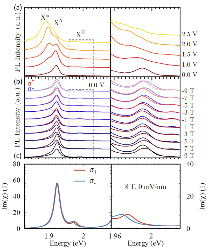
Fig. 3 a) depicts the evolution of the photoluminescence as a function of the applied gate voltage at 0T. Due to the lower energy of the XA transition, most of the luminescence stems from this mode. The PL from XH is quenched by approximately a factor of 10, but remains visible in the spectra (see right, zoomed panel). Evidently, when the bias voltage is raised up to 2.5 V, a third, red-shifted peak appears and eventually dominates the luminescence response the spectrum, which we assign to the charged intralayer excitonic state of the bilayer.
Importantly, as depicted in Fig. 3 b), a notable polarization splitting in both, the XA transition as well as the XH transition occurs in the presence of an applied magnetic field (here, no electric field is applied). A closer inspection indeed reveals, that this magnetic field splitting of the two modes displays an opposite sign, and a substantially modified magnitude: at -9T, the XA mode experiences a splitting of 0.8 meV, whereas the XH mode splitting exceeds -2 meV. To further quantify this behavior, we analyzed the extracted peak positions as a function of the applied magnetic field, yielding the g-factor of the XA exciton as -2. This, indeed, contrasts the commonly observed g-factors fluctuationg around -4 for A-excitons in TMDC monolayers, but we note that in particular in MoS2 monolayers, g-Factors of -2 have been reported goryca2019revealing ; cadiz2017excitonic . In our experiment, the g-factor of the hybrid XH , however, acquires a value of approx. 4.2. This already suggests that XA and XH are of fundamentally different character, and admix different valley contributions.
To investigate the Zeeman and Stark shifts of intra- and interlayer states more carefully, we carry out a microscopic analysis in the Heisenberg equation of motion framework. Starting point is the electronic bilayer Hamiltonian
| (1) |
The first term describes the dispersion of carriers in each monolayer constituting the bilayer. Here, accounts for the layer index, is for the band index, denotes the valley, denotes the spin and the momentum. The dispersion obeys the following symmetries
| (2) |
Here the notation accounts for the opposite valley to , i.e. . Similarly, accounts for the opposite band to , i.e. . We parametrize the electronic band structure of both individual monolayers by DFT calculations for monolayersKormanyos2015 . The second term term accounts for the tunneling of carriers between both layers , which is negligible for conduction band electrons but significant for the valence band, 38 meVdeilmann2018interlayer . The second line of the Hamiltonian accounts for light matter coupling. We assume a field propagation perpendicular to the bilayer, i.e. (only in-plane polarized excitons). We assume vanishing in-plane components of the interlayer dipole moment . Radiative coupling of intralayer excitons is taken into account via solving Maxwells equations in a planar geometrystroucken1996coherent . The third line in equation 1 accounts for the Coulomb coupling of the carriers. We neglect conduction band wavefunction overlap between the layers, i.e. we disregard Dexter coupling. The Coulomb coupling describes the formation interlayer excitons . The appearing Coulomb matrix element is given by an analytic solution of the static Poisson equationovesen2019interlayer incorporating the dielectric environment of the sample (2 layers embedded in hBN, ). It reads
| (3) |
with the dielectric function which accounts for Coulomb coupling within the layers or among different layers ovesen2019interlayer .
The first term in the fourth line of equation 1 accounts for Stark shifts of the electronic bands in the vicinity of a static out-of-plane electric field. For moderate electric fields (up to 1 V/nm), the shifts are linear as a function of the electric field, with a slope of 0.05 e nmdeilmann2018interlayer . Bands within the same layer shift in the same direction, but the bands of the different layer shift in opposite directiondeilmann2018interlayer . The last term accounts for the Zeeman shifts of the electronic states in an out-of-plane magnetic field. To the total magnetic moment three effects contributemacneill2015breaking
| (4) |
namely the spin contribution, the orbital contribution and the valley contribution:
-
•
the spin magnetic moment for gong2013magnetoelectric ; van2018strong : For optically allowed transitions the contributions of valence and conduction band cancel.
-
•
The orbital magnetic moment aivazian2015magnetic ; srivastava2015valley : In the monolayer, this contribution is responsible for the observed Zeeman shiftsmacneill2015breaking .
-
•
The valley magnetic moment yao2008valley ; xu2014spin : Since valence and conduction bands shift in the same direction, this contribution cancels almost for intralayer excitons with similar electron and holes masses.
-
•
The bilayer in AB stacking exhibits inversion symmetry. This implies, that the point in layer 1 underlies the same Zeeman shifts as the point in layer 2 and vice versa .
Next, we calculate the excitonic binding energies and wavefunctions for intra- and interlayer excitons by exploiting the Wannier equation and access the linear optical response via calculating the equation of motion for the exciton, as detailed in the supplementary material. Our calculations yield binding energies of 163 meV for intralayer and an encouragingly large binding energy of 112 meV for the interlayer A excitons.
Figure 3 illustrates the imaginary part of the dielectric susceptibility of the bilayer. Without the inclusion of the tunneling in the equation of motion (supplementary informations, equation 8) only the transition at 0 eV and transitions occur in the spectrum (see supplementary materials). Inclusion of the tunneling yields a weak resonance above the exciton, being associated with the interlayer exciton, forming an optically allowed transition through hybridization of intralayer and interlayer excitons.
Applying a magnetic field to our model in Figure 3 illustrates the polarization resolved dielectric susceptibility. Here, we consider a magnetic field of 8 T. We observe a splitting of all resonances, in particular the intralayer transitons exhibit a negative factor whereas the interlayer transition exhibits a positive one of much larger magnitude and opposite sign, clearly reproducing the phenomenological behavior captured in our experiment. A detailed analysis shows, that for the intralayer exciton, the valley contributions to the Zeeman shift for electron and hole almost cancel, and the total Zeeman shift is dictated by the orbital contribution. In contrast, for the interlayer transition, while electron and hole stem from different layers, the valley contribution is adding up. Additionally, while the hole is located in the other layer compared to the intralayer A transition, the orbital contribution has opposite sign, which adds up with the valley contribution.
The hybridization of energy bands, giving rise to the XH exciton resonance can be expected to sensible react on the precise mode energy (the detuning between the indicated transitions sketched in Fig. 1 c), and thus can be manipulated by the externally applied electric field. We check this hypothesis by repeating to determine the Zeeman-splittings for the captured manyparticle complexes for a variety of applied gate voltages Fig. 4 a)-d) and plot the extracted Zeeman-splittings as a function of the gate voltage: The trion emission indeed only displays a modest modification of the extracted g-factor, and the g-factor of the exciton XA fluctuates around a value of 2. More importantly, the hybrid exciton XH, which stands in the focus of this study, displays a progressive increase of the g-factor from 4.2 at 0 V up to 7 at 2.5 V (Fig. 4e).
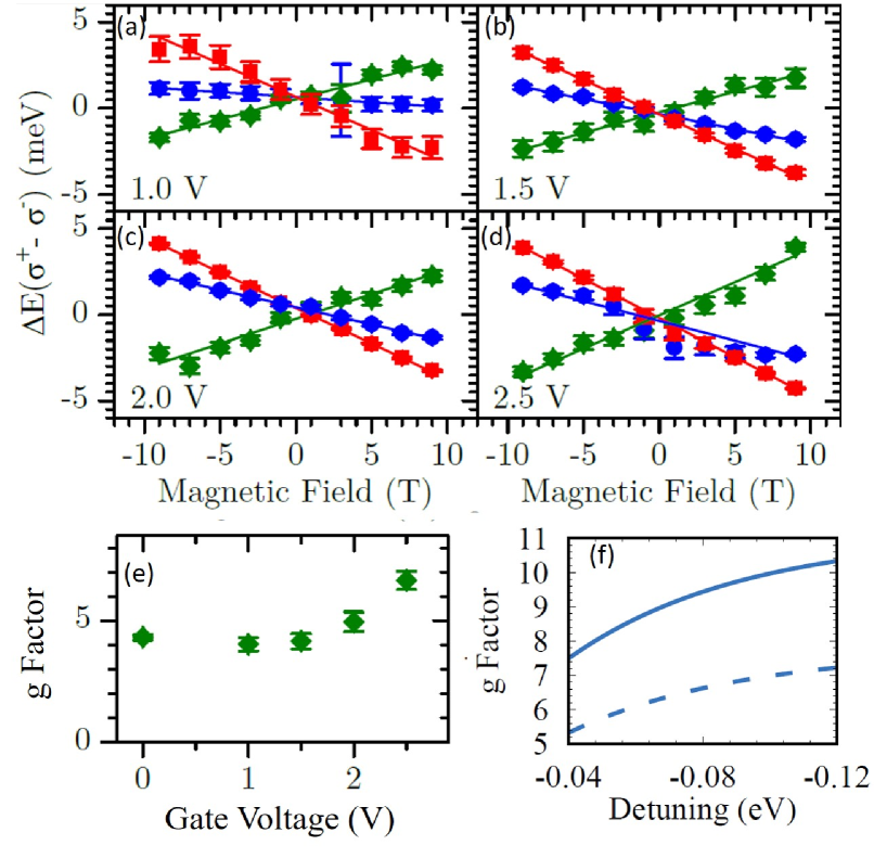
The reason for this behavior is the combined action of tunnel coupling of the interlayer excitons to the B exciton (which leads to a mixing of the g-factors) and the tuning of the energetic position of the interlayer exciton. Without coupling, let us assume first, that a pure interlayer exciton would have a g-factor of about 12 and the B exciton of about -3. We note, however, that in particular in the MoS2 system, strongly fluctuating g-factors are observed throughout the literature (those typically scatter between -2 and -4.5 for the A-exciton) goryca2019revealing ; cadiz2017excitonic , hinting at an utmost sensible dependence on the precise bandstructure which is sensibly reacting on the surrounding. Now, coupling between the B-exciton and the interlayer exciton leads to redistribution of the g factors among them, which becomes efficient if the interlayer exciton and the B exciton are weakly detuned. The applied electric field increases the detuning for the studied lower interlayer exciton from the B exciton resulting in an increasing g factor.
This can be phenomenologically captured in a simplified model including only the B exciton and one interlayer exciton . The simplified Bloch equations readkatsch2019theory
| (5) | |||
| (6) |
with the energies and and , . The new energies of these coupled oscillator equations are given as
| (7) | |||
| (8) |
where the solution refers to the transition and the lower solution refers to the interlayer transition. The effective factor is given as
| (9) |
We can now plot the effective factor as a function of the detuning in figure 4 f). We notice, despite a slight offset, the model captures the observed phenomenological behavior of the bias-tuneable factor of XH. Indeed, the quantitative deviation most likely arises from uncertainties associated with the g-factor of the (uncoupled) interlayer transition and the B-exciton, which are not experimentally accessible in our study. However, we notice that our A-interlayer exciton indeed displays factor of 2, rather than the canonical value of 4 captured for most other TMDC A-exciton complexes. Let us thus consider reduced factors of the B-exciton as well as the interlayer exciton, rescaled by a factor of 1.5. We note, that the dashed line depicted figure 4 f) manages to quantitatively capture the experimentally observed tuning range of the interlayer exciton can now qua and the interlayer exciton factor.
In conclusion, we have demonstrated the existence of an interlayer exciton in pristine bilayer MoS2, which is characterized by a giant dipole moment in conjunction with a persistent oscillator strength. We have analyzed the behavior of this new excitonic species in an applied external electric and magnetic field, and found evidence for the mixing of K and K‘ valley states, contributing to the exciton. The valley character is tunable in an externally applied electric field, by modifying the effective interlayer- vs. intralayer character.
Dipolar excitons with strong oscillator strength are of paramount importance for microcavity experiments in the regime of strong light-matter coupling. We anticipate, that the interlayer exciton in pristine bilayer MoS2 can be utilized to generate strongly interacting, dipolar exciton polaritons based on atomically thin materials.
During the preparation of the manuscript, we became aware of a an independent, similar work by Leisgang et al. arXiv:2002.02507 (2020).
Acknowledgements – The Würzburg group gratefully acknowledges support by the state of Bavaria. C.S. acknowledges funding with the ERC project unLiMIt-2D (Project No: 679288) and the DFG with the priority programm SPP 2244 (DFG SCHN1376 14.1). Technical support by M. Emmerling and A. Wolf is acknowledged. S.T. acknowledges support by the NSF (DMR-1955668 and DMR-1838443). We acknowledge fruitful discussions with our colleague Dominik Christiansen (TU Berlin). The TUB group was funded by the Deutsche Forschungsgemeinschaft via projects 182087777 in SFB 951 (project B12, M.S., and A.K.) and KN 427/11-1 (F.K. and A.K.). F.K. thanks the Berlin School of Optical Sciences and Quantum Technology.
Methods – Sample fabrication: MoS2 sheets were isolated from home-made flux zone grown MoS2 crystals. The process started with 6N purity metal powder (Mo) and sulfur ingot pieces. Additional care was given to performing in house purification to eliminate all the other contamination (typically heavy metals and magnetic metals) to reach true 6N purity. Crystal growth was performed using flux zone growth technique without any transporting agents to capture high quality crystals. The bilayers were then isolated using the dry transfer technique introduce in by Castellanos-Gomez et al. castellanos2014deterministic . we exfoliate our 2D materials on a transparent PolyDimethylSiloxane (PDMS) film. From this film, we transfer the 2D layers on a Si/SiO2 substrate (with 100 nm SiO2) with pre-patterned gold contact, that were initially deposited on the substrate via e-beam assisted evaporation.
References
- (1) Gang Wang, Alexey Chernikov, Mikhail M. Glazov, Tony F. Heinz, Xavier Marie, Thierry Amand, and Bernhard Urbaszek. Colloquium: Excitons in atomically thin transition metal dichalcogenides. Rev. Mod. Phys., 90:021001, Apr 2018.
- (2) John R Schaibley, Hongyi Yu, Genevieve Clark, Pasqual Rivera, Jason S Ross, Kyle L Seyler, Wang Yao, and Xiaodong Xu. Valleytronics in 2d materials. Nature Reviews Materials, 1(11):1–15, 2016.
- (3) Zhirui Gong, Gui-Bin Liu, Hongyi Yu, Di Xiao, Xiaodong Cui, Xiaodong Xu, and Wang Yao. Magnetoelectric effects and valley-controlled spin quantum gates in transition metal dichalcogenide bilayers. Nature Communications, 4:2053, 2013.
- (4) Ajit Srivastava, Meinrad Sidler, Adrien V Allain, Dominik S Lembke, Andras Kis, and A Imamoğlu. Valley zeeman effect in elementary optical excitations of monolayer wse 2. Nature Physics, 11(2):141–147, 2015.
- (5) Andreas V Stier, Kathleen M McCreary, Berend T Jonker, Junichiro Kono, and Scott A Crooker. Exciton diamagnetic shifts and valley zeeman effects in monolayer ws 2 and mos 2 to 65 tesla. Nature communications, 7(1):1–8, 2016.
- (6) Grant Aivazian, Zhirui Gong, Aaron M Jones, Rui-Lin Chu, Jiaqiang Yan, David G Mandrus, Chuanwei Zhang, David Cobden, Wang Yao, and Xiaodong Xu. Magnetic control of valley pseudospin in monolayer wse 2. Nature Physics, 11(2):148–152, 2015.
- (7) C Robert, B Han, P Kapuscinski, A Delhomme, C Faugeras, T Amand, M R Molas, M Bartos, K Watanabe, T Taniguchi, et al. Measurement of the Spin-Forbidden Dark Excitons in MoS2 and MoSe2 monolayers. arXiv preprint arXiv:2002.03877.
- (8) Alexey Chernikov, Timothy C. Berkelbach, Heather M. Hill, Albert Rigosi, Yilei Li, Ozgur Burak Aslan, David R. Reichman, Mark S. Hybertsen, and Tony F. Heinz. Exciton binding energy and nonhydrogenic rydberg series in monolayer . Phys. Rev. Lett., 113:076802, Aug 2014.
- (9) Qing Hua Wang, Kourosh Kalantar-Zadeh, Andras Kis, Jonathan N Coleman, and Michael S Strano. Electronics and optoelectronics of two-dimensional transition metal dichalcogenides. Nature nanotechnology, 7(11):699, 2012.
- (10) Nils Lundt, Sebastian Klembt, Evgeniia Cherotchenko, Simon Betzold, Oliver Iff, Anton V Nalitov, Martin Klaas, Christof P Dietrich, Alexey V Kavokin, Sven Höfling, et al. Room-temperature tamm-plasmon exciton-polaritons with a wse 2 monolayer. Nature communications, 7(1):1–6, 2016.
- (11) Xiaoze Liu, Tal Galfsky, Zheng Sun, Fengnian Xia, Erh-chen Lin, Yi-Hsien Lee, Stéphane Kéna-Cohen, and Vinod M Menon. Strong light–matter coupling in two-dimensional atomic crystals. Nature Photonics, 9(1):30, 2015.
- (12) Christian Schneider, Mikhail M Glazov, Tobias Korn, Sven Höfling, and Bernhard Urbaszek. Two-dimensional semiconductors in the regime of strong light-matter coupling. Nature communications, 9(1):1–9, 2018.
- (13) Pasqual Rivera, John R Schaibley, Aaron M Jones, Jason S Ross, Sanfeng Wu, Grant Aivazian, Philip Klement, Kyle Seyler, Genevieve Clark, Nirmal J Ghimire, et al. Observation of long-lived interlayer excitons in monolayer mose 2–wse 2 heterostructures. Nature communications, 6(1):1–6, 2015.
- (14) T. Stroucken, A. Knorr, P. Thomas, and S. W. Koch. Coherent dynamics of radiatively coupled quantum-well excitons. Physical Review B 53, 2026, 1996.
- (15) Iann C Gerber, Emmanuel Courtade, Shivangi Shree, Cedric Robert, Takashi Taniguchi, Kenji Watanabe, Andrea Balocchi, Pierre Renucci, Delphine Lagarde, Xavier Marie, et al. Interlayer excitons in bilayer mos 2 with strong oscillator strength up to room temperature. Physical Review B, 99(3):035443, 2019.
- (16) Andor Kormanyos, Guido Burkard, Martin Gmitra, Jaroslav Fabian, Viktor Zolyomi, Neil D Drummond, and Vladimir Falko. k p theory for two-dimensional transition metal dichalcogenide semiconductors. 2D Materials, 2(2):022001, 2015.
- (17) Thorsten Deilmann and Kristian Sommer Thygesen. Interlayer excitons with large optical amplitudes in layered van der waals materials. Nano letters, 18(5):2984–2989, 2018.
- (18) Simon Ovesen, Samuel Brem, Christopher Linderälv, Mikael Kuisma, Tobias Korn, Paul Erhart, Malte Selig, and Ermin Malic. Interlayer exciton dynamics in van der waals heterostructures. Communications Physics, 2(1):1–8, 2019.
- (19) David MacNeill, Colin Heikes, Kin Fai Mak, Zachary Anderson, Andor Kormányos, Viktor Zólyomi, Jiwoong Park, and Daniel C Ralph. Breaking of valley degeneracy by magnetic field in monolayer mose 2. Physical review letters, 114(3):037401, 2015.
- (20) M Van der Donck, M Zarenia, and F M Peeters. Strong valley Zeeman effect of dark excitons in monolayer transition metal dichalcogenides in a tilted magnetic field. Physical Review B, 97(8):081109, 2018.
- (21) Andor Kormányos, Viktor Zólyomi, Neil D Drummond, and Guido Burkard. Spin-orbit coupling, quantum dots, and qubits in monolayer transition metal dichalcogenides. Physical Review X, 4(1):011034, 2014.
- (22) Florian Katsch, Malte Selig, and Andreas Knorr. Theory of coherent pump–probe spectroscopy in monolayer transition metal dichalcogenides 2D Materials, 7, 015021, 2019.
- (23) Zhengguang Lu, Daniel Rhodes, Zhipeng Li, Dinh Van Tuan, Yuxuan Jiang, Jonathan Ludwig, Zhigang Jiang, Zhen Lian, Sufei Shi, James C Hone, Hanan Dery, and Dmitry Smirnov. Magnetic field mixing and splitting of bright and dark excitons in monolayer MoSe2. 2D Materials, 2019.
- (24) ZY Zhu, YC Cheng, and Udo Schwingenschlögl. Giant spin-orbit-induced spin splitting in two-dimensional transition-metal dichalcogenide semiconductors. Physical Review B, 84(15):153402, 2011.
- (25) Di Xiao, Gui-Bin Liu, Wanxiang Feng, Xiaodong Xu, and Wang Yao. Coupled spin and valley physics in monolayers of MoS2 and other group-VI dichalcogenides. Physical Review Letters, 108(19):196802, 2012.
- (26) Ting Cao, Gang Wang, Wenpeng Han, Huiqi Ye, Chuanrui Zhu, Junren Shi, Qian Niu, Pingheng Tan, Enge Wang, Baoli Liu, and Ji Feng. Valley-selective circular dichroism of monolayer molybdenum disulphide. Nature Communications, 3:887, 2012.
- (27) K Kośmider, Jhon W González, and Joaquín Fernández-Rossier. Large spin splitting in the conduction band of transition metal dichalcogenide monolayers. Physical Review B, 88(24):245436, 2013.
- (28) Agnieszka Kuc and Thomas Heine. The electronic structure calculations of two-dimensional transition-metal dichalcogenides in the presence of external electric and magnetic fields. Chemical Society Reviews, 44(9):2603, 2015.
- (29) Wang Yao, Di Xiao, and Qian Niu. Valley-dependent optoelectronics from inversion symmetry breaking. Physical Review B, 77(23):235406, 2008.
- (30) Xiaodong Xu, Wang Yao, Di Xiao, and Tony F Heinz. Spin and pseudospins in layered transition metal dichalcogenides. Nature Physics, 10(5):343, 2014.
- (31) Laturia, Akash and Van de Put, Maarten L and Vandenberghe, William G Dielectric properties of hexagonal boron nitride and transition metal dichalcogenides: from monolayer to bulk. npj 2D Materials and Applications, 2(1):1–7, 2018.
- (32) Wang, Zefang and Chiu, Yi-Hsin and Honz, Kevin and Mak, Kin Fai and Shan, Jie Electrical tuning of interlayer exciton gases in WSe2 bilayers Nano letters, 18(1):137–143, 2018.
- (33) Castellanos-Gomez, Andres and Buscema, Michele and Molenaar, Rianda and Singh, Vibhor and Janssen, Laurens and Van Der Zant, Herre SJ and Steele, Gary A Deterministic transfer of two-dimensional materials by all-dry viscoelastic stamping 2D Materials, 011002, 2014.
- (34) Goryca, M and Li, Jing and Stier, Andreas V and Taniguchi, Takashi and Watanabe, K and Courtade, Emmanuel and Shree, S and Robert, Cedric and Urbaszek, B and Marie, X and others Revealing exciton masses and dielectric properties of monolayer semiconductors with high magnetic fields Nature communications, 10(1) 1–12, 2019.
- (35) Cadiz, F and Courtade, E and Robert, Cédric and Wang, G and Shen, Y and Cai, H and Taniguchi, T and Watanabe, K and Carrere, H and Lagarde, D and others Excitonic linewidth approaching the homogeneous limit in MoS 2-based van der Waals heterostructures PRX, 021026, 2017.