Optically detected magnetic resonance in neutral silicon vacancy centers in diamond via bound exciton states
Abstract
Neutral silicon vacancy (SiV0) centers in diamond are promising candidates for quantum networks because of their excellent optical properties and long spin coherence times. However, spin-dependent fluorescence in such defects has been elusive due to poor understanding of the excited state fine structure and limited off-resonant spin polarization. Here we report the realization of optically detected magnetic resonance and coherent control of SiV0 centers at cryogenic temperatures, enabled by efficient optical spin polarization via previously unreported higher-lying excited states. We assign these states as bound exciton states using group theory and density functional theory. These bound exciton states enable new control schemes for SiV0 as well as other emerging defect systems.
Point defects in solid-state materials are promising candidates for quantum memories in a quantum network. These quantum defects combine the excellent optical and spin properties of isolated atoms with the scalability of solid-state systems Gao et al. (2015); Atatüre et al. (2018); Awschalom et al. (2018). Long-range, kilometer-scale entanglement generation has been demonstrated with the nitrogen vacancy (NV) center in diamond Hensen et al. (2015). However, the entanglement generation rate in such demonstrations is limited by the optical properties of the NV center, which exhibits significant spectral diffusion Wolters et al. (2013); Chu et al. (2014) and a small Debye-Waller factor Barclay et al. (2011). The neutral silicon vacancy center in diamond (SiV0) has the potential to mitigate many of these problems; its inversion symmetry guarantees a vanishing permanent dipole moment, which minimizes spectral diffusion, and over 90 of its emission is in the zero-phonon line (ZPL) Rose et al. (2018a). However, there has been no report of optically detected magnetic resonance (ODMR) for this defect, a key first step towards establishing a spin-photon interface, and the electronic structure of SiV0 is still not well understood Green et al. (2019). A detailed understanding of the optical transition and excited state structure of SiV0 is key in developing preparation, manipulation and readout schemes for quantum information processing applications.
In this work, we present the observation of previously unreported optical transitions in SiV0 that are capable of efficiently polarizing the ground state spin. Previous studies on SiV0 have reported a strong ZPL transition at 946 nm, and a weaker strain-activated transition at 951 nm Green et al. (2019). Through a combination of optical and electron spin resonance (ESR) measurements, we are able to assign groups of transitions from 825 to 890 nm to higher-lying excited states of SiV0. We interpret these spectroscopic lines as transitions to bound exciton (BE) states of the defect. We observe highly efficient bulk spin polarization through optical excitation of these transitions, providing another manifold of states that can be used for spin initialization. Spin polarization via these BE states while collecting emission from the ZPL and phonon sideband enables the observation of ODMR. We use ODMR measurements to probe the low magnetic field behavior of SiV0 where we observe no spin relaxation () out to 30 ms, spin dephasing times () of 202 ns, and spin coherence times () of 55.5 s at 6 K.
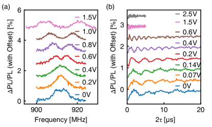
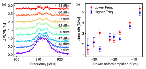
We observe ODMR in an ensemble of SiV0 centers using excitation at one of the BE transitions (855.65 nm) in a chemical-vapor deposition grown sample doped with isotopically enriched 29Si during growth, described previously in Ref. Rose et al. (2018b). As the microwave frequency is swept across the zero-field splitting of SiV0, we observe three resonance peaks in continuous-wave (CW) ODMR [Fig. 1(a)]. The two outer peaks correspond to spin transitions associated with centers containing 29Si, while the central peak at 944 MHz is associated with 28Si and 30Si. The position and splitting of the lines are consistent with previously measured hyperfine parameters Edmonds et al. (2008).
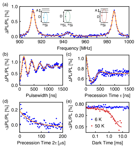
We realize coherent control using pulsed ODMR on the lower frequency 29Si hyperfine transition at 912 MHz and observe Rabi oscillations that decay over 499 ns [Fig. 1(b)]. We measure the spin dephasing time to be ns [Fig. 1(c)] using a Ramsey sequence. By using a Hahn echo sequence to refocus the coherence, we measure the spin coherence time to be s [Fig. 1(d)]. The spin coherence time measured here is shorter than previous measurements of this sample using -band pulsed ESR, s Rose et al. (2018b). This likely arises from the high density of SiV0 centers in this sample, which gives rise to instantaneous diffusion Tyryshkin et al. (2012); Rose et al. (2018b). At ambient magnetic fields, the effects of instantaneous diffusion are more pronounced because centers of different orientations and nuclear spin projections are nearly degenerate. This effect limits to 56 s (see Supplemental Material Sec. III B Sup ).
We measure the spin relaxation time () using pulsed ODMR by measuring spin population decay after a variable dark time between the initialization and readout pulses. We observe no decay up to 30 ms at 6 K [Fig. 1(e)], consistent with previous measurements of s at this temperature Rose et al. (2018b). At higher temperatures, the spin lifetime shortens significantly due to an Orbach process with an activation energy of 16.8 meV Rose et al. (2018b) and we measure ms at 50 K.
Our temperature-dependent ODMR measurements on the lower hyperfine transition are consistent with the previously measured activation energy (see Fig. S7 Sup ), but we observe the Orbach rate prefactor to be 260 times larger. This is largely due to hyperfine-induced mixing of the SiV0 spin states (see Supplemental Material Sec. III C Sup ). The hyperfine interaction for SiV0 is 30 times larger than that for the NV center and the zero-field splitting is three times smaller Edmonds et al. (2008); Felton et al. (2009), so at low magnetic field the influence of the hyperfine interaction is much more pronounced. Unlike nitrogen, however, silicon has spin-free nuclear isotopes which may be used to circumvent these effects.
The observation of ODMR in SiV0 is enabled by the discovery of additional higher-lying excited states beyond the ZPL. Previous studies on SiV0 excited states were limited to the (ZPL at 946 nm) and (ZPL at 951 nm) states but higher energy states were never explored. Transitions between 820 and 950 nm in silicon-doped diamonds have been previously observed with photoconductivity and absorption measurements, but there has been no detailed spectroscopy of these spectral lines, nor assignment of their microscopic origin Allers and Collins (1995); D’Haenens-Johansson et al. (2010, 2011).
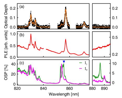
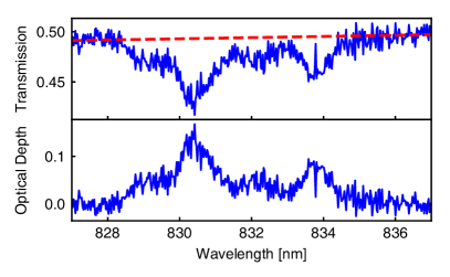
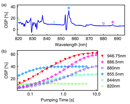
In order to probe whether these transitions are associated with the SiV0 center, we correlate several types of optical spectroscopy at low temperature (5.5 K) at ambient magnetic field. First we perform absorption spectroscopy over a large wavelength range, from the ionization threshold (826 nm Allers and Collins (1995)) to 900 nm. We observe several families of peaks near 830, 855, and 870 nm [Fig. 2(a)]. Then we perform photoluminescence excitation (PLE) spectroscopy, wherein we excite at these absorption wavelengths and detect emission at 946 nm, the ZPL of SiV0. We observe the same clusters of resonances in PLE, confirming that the transitions are associated with the SiV0 center [Fig. 2(b)].
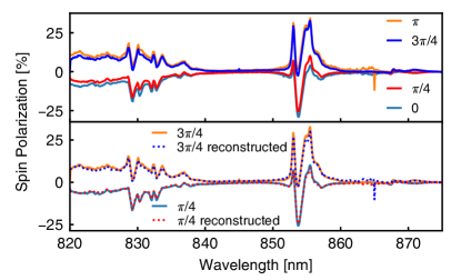
Finally, we probe the interaction between these higher lying transitions and the ground state spin of SiV0 by measuring optical spin polarization (OSP) in bulk ESR (3100 G) after excitation at these wavelengths [Fig. 2(c)]. Specifically, we use a pump-probe measurement to isolate the contributions from () and () spin states (see Supplemental Material Sec. VI Sup ). Remarkably, the bulk OSP reaches values up to (see Supplemental Material Sec. V Sup ), a key enabling capability for the observation of ODMR.
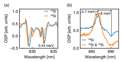
Using OSP measurements, we also observe a new cluster of transitions near 886 nm that are not evident in absorption or PLE spectroscopy [Fig. 2(c), right]. This indicates that these transitions have a weak oscillator strength, but are strongly spin polarizing.
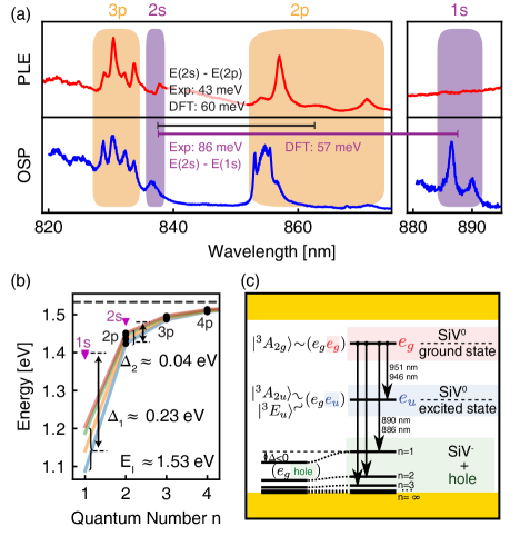
The number of observed transitions cannot be described by models utilizing only the orbitals localized on the SiV0 center. Group theoretic considerations describe three triplet excited configurations for SiV0: , and Gali and Maze (2013). Bulk photoluminescence measurements under uniaxial stress suggest that the 946 nm transition arises from the state and the 951 nm transition arises from the state Green et al. (2019). Only the transition from the state has not been experimentally identified.
The proximity of several of these resonances to the ionization threshold of SiV0 (826 nm Allers and Collins (1995)) provides a clue to their nature. We propose that SiV0 can act as a pseudo-acceptor, forming BE states composed of a hole weakly bound to a transiently generated SiV- center. BE states of neutral defects have been observed in SiC Egilsson et al. (1999); Storasta et al. (2001), Si Wagner et al. (1985); Kleverman et al. (1988); Svensson et al. (1990); Frens et al. (1994); Son et al. (1994), and GaP Pressel et al. (1993). One manifestation of BE states is a progression of peaks that can be described qualitatively as transitions between hydrogenic states and labeled with principal quantum numbers, , and angular momentum labels (, , , etc.). These progressions are observed in both PLE and OSP measurements, shown in Fig. 3(a). A schematic level diagram for the states described here is depicted in Fig. 3(c). Based on this model, transitions to “”-like states are expected to be electric-dipole forbidden, since both the ground state and BE state are of symmetry. Indeed, we observe transitions at 886 and 837 nm in OSP, but not in absorption or PLE. The isotopic shift of the transition suggests that this transition is phonon assisted in nature (see Supplemental Material Sec. VII Sup ). We fit the observed energies () of the “”-like transitions to the Rydberg scaling, , shown in Fig. 3(b), where is the ionization energy and is the Rydberg energy. We find the fitted ionization energy to be in good agreement with photoconductivity measurements Allers and Collins (1995), and the Rydberg energy to be consistent with an effective-mass description of the system (see Supplemental Material Sec. VIII A Sup ).
The -like states were excluded from this analysis because of their vibronic nature and the central-cell correction expected for these types of states Cardona and Peter (2005). This expectation is borne out in density functional theory (DFT) calculations (see Fig. S20 and Supplemental Material Sec. IX G Sup ), where the calculated - energy difference of 57 meV is in better agreement with experimental measurements (86 meV) than the meV difference expected from a hydrogenic model without a central cell correction. The calculated energy difference between the and states is also consistent with experimental observations [Fig. 3(a)]. The central cell correction arises because the BE states are effectively excluded from occupying the 6 carbon atoms adjacent to the SiV- center, increasing the effective Bohr radius and decreasing the effective Rydberg energy. This effect is less pronounced for -like states because they have radial nodes at the SiV- center.
Within each labeled manifold in Fig. 3(a), significant structure is observed. This likely arises from a combination of spin-orbit structure in the valence band, crystal-field interactions from the presence of the symmetry-lowering SiV0 defect, and coupling between the bound hole and SiV-. We note that the bulk inhomogeneous linewidth likely obscures the full multiplicity of these transitions.
Transitions above the level are not clearly observable in the experimental data. We believe this is a combination of the oscillator strength scaling (), proximity to the ionization threshold, and competition with other nonradiative, non-spin-polarizing relaxation pathways.
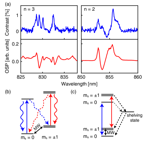
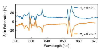
With this model for the nature of the transitions, we now turn to the details of the spin polarization and ODMR contrast. The magnitude of the ODMR signal depends sensitively on the excitation wavelength, and we observe resonant features that match the linewidths observed in absorption, PLE, and OSP measurements for the and BE transitions [Fig. 4(a), upper panel]. This is in stark contrast to ODMR in the NV center, which shows significant ODMR contrast for off-resonant excitation due to its spin dependent intersystem crossing. This indicates that the mechanism for ODMR relies on selective excitation of these transitions, which can arise from both the resonant nature of OSP and spin-selective optical pumping leading to population shelving into a “dark” spin state.
Furthermore, we observe that the ODMR signal can be both positive and negative. Optical transitions with nonunity cyclicity lead to population of ground states (e.g., other levels here) that are not addressed by the spectrally narrow excitation [Fig. 4(b)]. This process has no preferential direction of spin-polarization (addressing different optical transitions may result in net polarization in either or ), but should result in positive contrast (brighter emission) under resonant microwave driving, as population is restored to the state being addressed by the optical excitation.
Another possible mechanism involves spin-dependent shelving of population in the excited state into a metastable state, which then decays back to the ground state [Fig. 4(c)]. This mechanism is observed in the NV center under off-resonant excitation at room temperature. Here, the excitation addresses all spin sublevels in the ground state, and the different branching ratios in the excited state for different spin projections result in a spin polarization direction independent of excitation wavelength Robledo et al. (2011). The sign of the ODMR contrast, however, has no such general restriction, and should depend on the specific details of the excited state manifold.
We compare the OSP and the ODMR contrast for the and BE transitions in Fig. 4(a). Spin polarization both into and out of the state is observed, depending on the excitation wavelength. This suggests that optical pumping plays a role in the excitation cycle of these transitions. The ODMR contrast data, however, reveals that this is not a complete description. Although the data shows primarily positive contrast (brighter emission), the data shows clear negative contrast for some excitation wavelengths. This suggests that decay from the excited state into a different manifold of states is involved.
In conclusion, we report the first realization of ODMR in SiV0 centers in diamond. We demonstrate coherent control of an ensemble of SiV0 spins at low magnetic field and measure much longer than 30 ms and of 55.5 s at 6 K. ODMR is enabled by newly discovered higher-lying excited states of SiV0, which allow for efficient optical spin polarization. We propose that these transitions arise from BE states, and we provide DFT calculations for the ionization threshold, central cell correction, and energy splitting between different states that are consistent with experimental observations. On-going work includes single center ODMR measurements, as well as investigating the microscopic mechanism for ODMR via BE states. Our measurements indicate that ODMR cannot arise solely from spin-dependent shelving of population or resonant optical pumping into a dark state, and it is likely that a combination of processes give rise to the observed features.
Optical spin polarization via these BE states enables a powerful method of spin initialization and readout for SiV0 centers in diamond. In particular, their resonant nature allows for the use of much lower excitation powers, which circumvents optically induced noise from the bath Siyushev et al. (2013). More broadly, this scheme can potentially be deployed in other emerging defect systems, such as other neutral group IV vacancy centers in diamond Thiering and Gali (2018, 2019) and neutral divacancy centers in SiC Koehl et al. (2011).
We thank J. Thompson for fruitful discussions, as well as S. Kolkowitz, L. Rodgers, and Z. Yuan for comments on the manuscript. This work was supported by the NSF under the EFRI ACQUIRE program (Grant No. 1640959) and through the Princeton Center for Complex Materials, a Materials Research Science and Engineering Center (Grant No. DMR-1420541). This material is also based on work supported by the Air Force Office of Scientific Research under Grant No. FA9550-17-0158, and was partly supported by DARPA under Grant No. D18AP00047. G. T. was supported by the János Bolyai Research Scholarship of the Hungarian Academy of Sciences and the ÚNKP-20-5 New National Excellence Program of the Ministry of Innovation and Technology in Hungary (ITM) from the National Research, Development and Innovation Office in Hungary (NKFIH). D. H. was supported by a National Science Scholarship from A*STAR, Singapore. A. G. acknowledges the support from NKFIH for Quantum Technology Program (Grant No. 2017-1.2.1-NKP-2017-00001) and National Excellence Program (Grant No. KKP129866), from the ITM and NKFIH for the Quantum Information National Laboratory in Hungary, from the EU Commission (Asteriqs project, Grant No. 820394) and the EU QuantERA program (Q_magine project, NKFIH Grant No. 127889).
References
- Gao et al. (2015) W. B. Gao, A. Imamoglu, H. Bernien, and R. Hanson, Nature Photonics 9, 363 (2015).
- Atatüre et al. (2018) M. Atatüre, D. Englund, N. Vamivakas, S.-Y. Lee, and J. Wrachtrup, Nature Reviews Materials 3, 38 (2018).
- Awschalom et al. (2018) D. D. Awschalom, R. Hanson, J. Wrachtrup, and B. B. Zhou, Nature Photonics 12, 516 (2018).
- Hensen et al. (2015) B. Hensen, H. Bernien, A. E. Dréau, A. Reiserer, N. Kalb, M. S. Blok, J. Ruitenberg, R. F. L. Vermeulen, R. N. Schouten, C. Abellán, W. Amaya, V. Pruneri, M. W. Mitchell, M. Markham, D. J. Twitchen, D. Elkouss, S. Wehner, T. H. Taminiau, and R. Hanson, Nature 526, 682 (2015).
- Wolters et al. (2013) J. Wolters, N. Sadzak, A. W. Schell, T. Schröder, and O. Benson, Physical Review Letters 110, 027401 (2013).
- Chu et al. (2014) Y. Chu, N. P. de Leon, B. J. Shields, B. Hausmann, R. Evans, E. Togan, M. J. Burek, M. Markham, A. Stacey, A. S. Zibrov, A. Yacoby, D. J. Twitchen, M. Loncar, H. Park, P. Maletinsky, and M. D. Lukin, Nano Letters 14, 1982 (2014).
- Barclay et al. (2011) P. E. Barclay, K.-M. C. Fu, C. Santori, A. Faraon, and R. G. Beausoleil, Physical Review X 1, 011007 (2011).
- Rose et al. (2018a) B. C. Rose, D. Huang, Z.-H. Zhang, P. Stevenson, A. M. Tyryshkin, S. Sangtawesin, S. Srinivasan, L. Loudin, M. L. Markham, A. M. Edmonds, D. J. Twitchen, S. A. Lyon, and N. P. de Leon, Science 361, 60 (2018a).
- Green et al. (2019) B. L. Green, M. W. Doherty, E. Nako, N. B. Manson, U. F. S. D’Haenens-Johansson, S. D. Williams, D. J. Twitchen, and M. E. Newton, Physical Review B 99, 161112 (2019).
- Rose et al. (2018b) B. C. Rose, G. Thiering, A. M. Tyryshkin, A. M. Edmonds, M. L. Markham, A. Gali, S. A. Lyon, and N. P. de Leon, Physical Review B 98, 235140 (2018b).
- Edmonds et al. (2008) A. M. Edmonds, M. E. Newton, P. M. Martineau, D. J. Twitchen, and S. D. Williams, Physical Review B 77, 245205 (2008).
- (12) See Supplemental Material for methods, additional characterization data, theoretical descriptions and calculations.
- Tyryshkin et al. (2012) A. M. Tyryshkin, S. Tojo, J. J. L. Morton, H. Riemann, N. V. Abrosimov, P. Becker, H.-J. Pohl, T. Schenkel, M. L. W. Thewalt, K. M. Itoh, and S. A. Lyon, Nature Materials 11, 143 (2012).
- Felton et al. (2009) S. Felton, A. M. Edmonds, M. E. Newton, P. M. Martineau, D. Fisher, D. J. Twitchen, and J. M. Baker, Physical Review B 79, 075203 (2009).
- Allers and Collins (1995) L. Allers and A. T. Collins, Journal of Applied Physics 77, 3879 (1995).
- D’Haenens-Johansson et al. (2010) U. F. S. D’Haenens-Johansson, A. M. Edmonds, M. E. Newton, J. P. Goss, P. R. Briddon, J. M. Baker, P. M. Martineau, R. U. A. Khan, D. J. Twitchen, and S. D. Williams, Physical Review B 82, 155205 (2010).
- D’Haenens-Johansson et al. (2011) U. F. S. D’Haenens-Johansson, A. M. Edmonds, B. L. Green, M. E. Newton, G. Davies, P. M. Martineau, R. U. A. Khan, and D. J. Twitchen, Physical Review B 84, 245208 (2011).
- Gali and Maze (2013) A. Gali and J. R. Maze, Physical Review B 88, 235205 (2013).
- Egilsson et al. (1999) T. Egilsson, J. P. Bergman, I. G. Ivanov, A. Henry, and E. Janzén, Physical Review B 59, 1956 (1999).
- Storasta et al. (2001) L. Storasta, F. H. C. Carlsson, S. G. Sridhara, J. P. Bergman, A. Henry, T. Egilsson, A. Hallén, and E. Janzén, Applied Physics Letters 78, 46 (2001).
- Wagner et al. (1985) J. Wagner, A. Dörnen, and R. Sauer, Physical Review B 31, 5561 (1985).
- Kleverman et al. (1988) M. Kleverman, J.-O. Fornell, J. Olajos, H. G. Grimmeiss, and J. L. Lindström, Physical Review B 37, 10199 (1988).
- Svensson et al. (1990) J. H. Svensson, B. Monemar, and E. Janzén, Physical Review Letters 65, 1796 (1990).
- Frens et al. (1994) A. M. Frens, M. T. Bennebroek, A. Zakrzewski, J. Schmidt, W. M. Chen, E. Janzén, J. L. Lindström, and B. Monemar, Physical Review Letters 72, 2939 (1994).
- Son et al. (1994) N. T. Son, M. Singh, J. Dalfors, B. Monemar, and E. Janzén, Physical Review B 49, 17428 (1994).
- Pressel et al. (1993) K. Pressel, A. Dörnen, G. Rückert, and K. Thonke, Physical Review B 47, 16267 (1993).
- Cardona and Peter (2005) M. Cardona and Y. Y. Peter, Fundamentals of semiconductors (Springer, 2005).
- Robledo et al. (2011) L. Robledo, H. Bernien, T. van der Sar, and R. Hanson, New Journal of Physics 13, 025013 (2011).
- Siyushev et al. (2013) P. Siyushev, H. Pinto, M. Vörös, A. Gali, F. Jelezko, and J. Wrachtrup, Physical Review Letters 110, 167402 (2013).
- Thiering and Gali (2018) G. Thiering and A. Gali, Physical Review X 8, 021063 (2018).
- Thiering and Gali (2019) G. Thiering and A. Gali, npj Computational Materials 5, 18 (2019).
- Koehl et al. (2011) W. F. Koehl, B. B. Buckley, F. J. Heremans, G. Calusine, and D. D. Awschalom, Nature 479, 84 (2011).
- Green et al. (2017) B. L. Green, S. Mottishaw, B. G. Breeze, A. M. Edmonds, U. F. S. D’Haenens-Johansson, M. W. Doherty, S. D. Williams, D. J. Twitchen, and M. E. Newton, Physical Review Letters 119, 096402 (2017).
- Dietrich et al. (2014) A. Dietrich, K. D. Jahnke, J. M. Binder, T. Teraji, J. Isoya, L. J. Rogers, and F. Jelezko, New Journal of Physics 16, 113019 (2014).
- Komsa et al. (2012) H.-P. Komsa, T. T. Rantala, and A. Pasquarello, Physical Review B 86, 045112 (2012).
- Makov and Payne (1995) G. Makov and M. C. Payne, Physical Review B 51, 4014 (1995).
- Freysoldt et al. (2009) C. Freysoldt, J. Neugebauer, and C. G. Van de Walle, Physical Review Letters 102, 016402 (2009).
- Lany and Zunger (2008) S. Lany and A. Zunger, Physical Review B 78, 235104 (2008).
- Wu and Fisher (2008) W. Wu and A. J. Fisher, Physical Review B 77, 045201 (2008).
- Luttinger and Kohn (1955) J. M. Luttinger and W. Kohn, Physical Review 97, 869 (1955).
- Kittel and Mitchell (1954) C. Kittel and A. H. Mitchell, Physical Review 96, 1488 (1954).
- Kohn and Luttinger (1955) W. Kohn and J. M. Luttinger, Physical Review 98, 915 (1955).
- Collins (1993) A. T. Collins, Philosophical Transactions of the Royal Society of London. Series A: Physical and Engineering Sciences 342, 233 (1993).
- Rauch (1962) C. J. Rauch, in Proceedings of the International Conference on the Physics of Semiconductors, edited by A. C. Stickland (Institute of Physics and the Physical Society of London, 1962) pp. 276–280.
- Herman et al. (1963) F. Herman, C. D. Kuglin, K. F. Cuff, and R. L. Kortum, Physical Review Letters 11, 541 (1963).
- Serrano et al. (1999) J. Serrano, A. Wysmolek, T. Ruf, and M. Cardona, Physica B: Condensed Matter 273-274, 640 (1999).
- Willatzen et al. (1994) M. Willatzen, M. Cardona, and N. E. Christensen, Physical Review B 50, 18054 (1994).
- Ashcroft and Mermin (1976) N. W. Ashcroft and N. D. Mermin, Solid state physics (New York: Holt, Rinehart and Winston, 1976).
- Gali et al. (2009) A. Gali, E. Janzén, P. Deák, G. Kresse, and E. Kaxiras, Physical Review Letters 103, 186404 (2009).
- Londero et al. (2018) E. Londero, G. Thiering, L. Razinkovas, A. Gali, and A. Alkauskas, Physical Review B 98, 035306 (2018).
- Kresse and Furthmüller (1996) G. Kresse and J. Furthmüller, Physical Review B 54, 11169 (1996).
- Steiner et al. (2016) S. Steiner, S. Khmelevskyi, M. Marsmann, and G. Kresse, Physical Review B 93, 224425 (2016).
- Blöchl (1994) P. E. Blöchl, Physical Review B 50, 17953 (1994).
- Bengone et al. (2000) O. Bengone, M. Alouani, P. Blöchl, and J. Hugel, Physical Review B 62, 16392 (2000).
- Heyd et al. (2003) J. Heyd, G. E. Scuseria, and M. Ernzerhof, The Journal of Chemical Physics 118, 8207 (2003).
- Krukau et al. (2006) A. V. Krukau, O. A. Vydrov, A. F. Izmaylov, and G. E. Scuseria, The Journal of Chemical Physics 125, 224106 (2006).
- Perdew et al. (1996) J. P. Perdew, K. Burke, and M. Ernzerhof, Physical Review Letters 77, 3865 (1996).
Supplemental Material for
“Optically detected magnetic resonance in neutral silicon vacancy centers in diamond via bound exciton states”
I SUPPLEMENTARY EXPERIMENTAL METHODS
I.1 Experimental Setups
Sample preparation: Three different {110} diamonds grown by chemical vapor deposition were studied. The first two samples (D1 and D2) were doped during growth with silicon. The silicon precursor was isotopically enriched with 90% 29Si (resulting in similar residual concentration of 28Si and 30Si). After high-pressure-high-temperature annealing, the SiV0 concentration is cm-3 for sample D1 Rose et al. (2018b). Sample D2 was cut along the growth direction so its SiV0 concentration depends on the specific region under study. We estimate its SiV0 concentration to be cm-3 for the region studied in photoluminescence excitation (PLE) measurements. The third diamond (D3) was doped during growth with boron and implanted with 28Si, as described in Rose et al. (2018a). After annealing, the resulting SiV0 concentration in the implanted layer is cm-3. Sample D1 is studied in the main text while samples D2 and D3 are measured to provide additional data in the supplemental material. Sample D1 shows a preferential alignment of SiV0 such that the in-plane and out-of-plane sites have a density ratio of 1:3 D’Haenens-Johansson et al. (2011).
Electron spin resonance (ESR): Pulsed X-band (9.5 GHz) ESR is performed on a modified Bruker Elexsys 580 system using a dielectric volume resonator (Bruker MD5) and a 1.4-T electromagnet, the details of which are thoroughly described elsewhere Rose et al. (2018b). Optical illumination is applied through a multi-mode fiber (Thorlabs FT400EMT) positioned above the sample. A narrow linewidth tunable CW Ti:Sapphire laser (Msquared SolsTis) is used as the excitation source for 800 nm - 1000 nm. For pump-probe ESR measurements, a second narrow linewidth tunable laser (Toptica CTL 950) is used as the pumping laser. All measurements are performed on the transition with the magnetic field aligned to a direction of the sample unless otherwise noted. Optical spin polarization (OSP) is measured using a two-pulse Hahn echo sequence (200 ns pulse) after optical excitation. The echo intensity is normalized to the echo intensity resulting from thermal polarization in the dark. The sign of OSP is defined as the relative population of the spin levels, with positive (negative) OSP being more polarization into () state. OSP is measured on the 29Si hyperfine line for samples D1 and D2 unless otherwise noted. All ESR measurements are performed at 5.5 K.
Photoluminescence excitation (PLE): All optical measurements are performed in a helium flow cyrostat (Janis ST-100) with the sample mounted on a copper cold finger. Excitation and detection channels for PLE are separated by a dichroic beam splitter (Semrock FF924-Di01). Excitation is focused on the sample with a 30 mm doublet lens. Emission is further filtered with a tunable 937 nm long-pass filter (Semrock FF01-937/LP-25) and coupled to a 50 m multimode fiber that routes the signal to a grating spectrometer (Princeton Instruments Acton SP-2300i). At each excitation wavelength, we acquire a photoluminescence (PL) spectrum and plot integrated emission at the 946 nm peak.
Absorption: For absorption measurements, the laser is split into two paths. One path travels through both the diamond and the windows of the cryostat while the other travels through only the windows of the cryostat, serving as a reference. Transmitted power through each path is measured with a Si photodiode (Thorlabs DET100A). The thickness of the diamond sample (D1) used for absorption is 0.66 mm.
Optically detected magnetic resonance (ODMR): For ODMR, the laser is coupled to an acousto-optic modulator (AOM, Isomet 1305C-1) for pulsed excitation. ODMR experiments use the same optical setup as PLE except that the signal is sent to a single photon detector (Excelitas SPCM-AQRH) and the excitation is focused on the sample with a 10X near infrared objective (Olympus LMPLN10XIR) outside of the cryostat. Microwave (MW) excitation is applied using a 70 m wire stretched across the sample. The MW excitation is generated with a signal generator (Rohde and Schwarz SMATE200A) and then amplified by a high-power MW amplifier (Ophir 5144). Two 0.8 - 2 GHz MW circulators (Ditom D3C0802S) are added after the amplifier for circuit protection. The MW excitation is pulsed using a fast MW switch (Mini-Circuits ZASWA-2-50DR+). The timing of MW pulses and optical pulses are synchronized using a TTL pulse generator (SpinCore PBESR-PRO-500). A home-built Helmholtz coil is used to apply a magnetic field along one of the in-plane directions. For time-tagging the photon counts, a time-correlated single photon counting system (PicoQuant PicoHarp 300) is used.
I.2 ESR Pulse Sequences

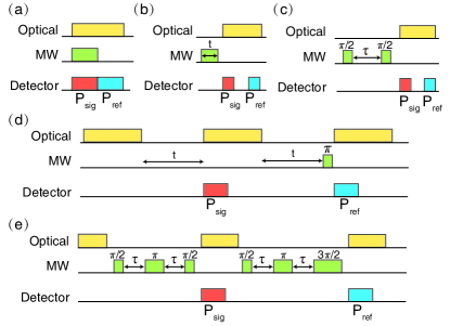
In pulsed ESR, the echo intensity is proportional to the population difference of the two spin levels under study. Spin polarization is measured by monitoring the integrated echo intensity from a standard Hahn-echo sequence after an optical pump pulse [Fig. S1(a)]. For state-resolved measurements, the spins are first initialized into with a long optical pump pulse at 946.76 nm to achieve efficient OSP from ZPL excitation. For initialization, a MW pulse is then applied to invert the population. After initialization, a short optical probe pulse is applied [Fig. S1(b)]. For data shown in Fig. 2(c), the length of the optical pump pulse (80 mW excitation power) is 6 s for measurements between 820 nm to 875 nm, and 4 s for measurements between 880 nm and 895 nm. The length of the optical probe pulse (45 mW excitation power) is 100 ms for measurements between 820 nm and 875 nm, and 500 ms for measurements between 880 nm and 895 nm. Polarization saturation curves are measured by shining an optical pump pulse with different pulse lengths. To avoid waiting for the spins to reset after each pulse sequence, an off-resonant optical pulse and N evenly spaced pulses are applied to scramble the spin polarization before the pump pulse [Fig. S1(c)]. For these measurements, N=6. The analysis for these data is described in Section V and Section VI.
I.3 ODMR Pulse Sequences
To suppress slow noise in continuous-wave (CW) ODMR measurements, we modulate the MW pulses on and off at a rate of 1 kHz. Photon counts are gated when the MW tone is on () and off (), and ODMR contrast is normalized using [Fig. S2(a)].
For pulsed ODMR measurements, the large dynamic range of laser pulse duty cycle gives rise to systematic fluctuations in the laser power because of AOM heating. To correct for this effect, we use two types of normalization for pulsed ODMR experiments. For Rabi and measurements where the laser is gated mostly on, we use a standard detection scheme [Fig. S2(b) and Fig. S2(c)]. Two 10 s detection windows separated by 50 s are applied during the readout pulse. The first window measures the transient spin population () after the MW pulses while the second window measures the steady state spin population (). The normalized signal is calculated as .
For and measurements where the duty cycle varies significantly with delay time, we alternately apply different microwave pulses before the readout pulse to invert the phase of detection. For , we alternate between applying a pulse and not applying any MW pulse in order to provide a reference count rate [Fig. S2(d)]. This also ensures the timescale we measure is related to the spin-relaxation, and does not include contributions from other optical processes. For , we alternate between applying a pulse or a pulse [Fig. S2(e)]. The data taken with phase inversion is normalized as .
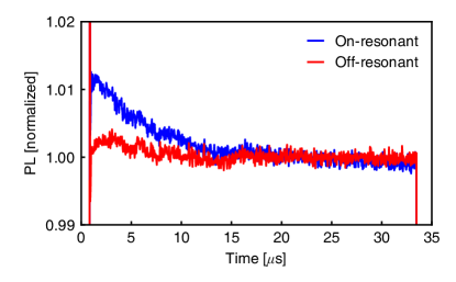
I.4 Transient Spin-dependent Fluorescence
To determine the optimum integration window for ODMR measurements, we measure transient spin-dependent PL by time-tagging the photon counts. A long optical pulse (30 s) first polarizes the spin ensemble. Then we apply an on-resonant (off-resonant) MW pulse to flip (not flip) the spin state. The time traces for different spin states are shown in Fig. S3. We observe spin-dependent PL up to 15 s. The integration windows and optical pulse duration are set accordingly: we set the spin polarization time to 75 s, and we set the detection window to 10 s.
II Additional Characterization on Multiple Samples
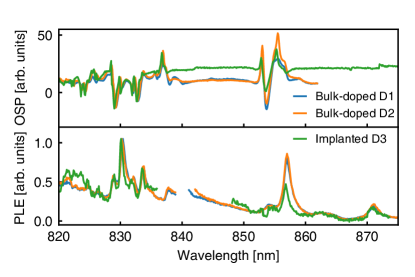
To confirm that the higher-lying excited states are a feature intrinsic to SiV0 centers rather than some sample dependent phenomenon, we measure OSP and PLE on two bulk-doped samples (D1 and D2) and a third implanted sample, D3.
The spectra show consistent optical transitions and spin polarization behavior (Fig. S4). An isotopic shift is observed between D1, D2 (29Si enriched) and D3 (28Si implanted), arising from differences in the zero-point energy of the local phonons.
III Low-Field Spin Dynamics
III.1 Magnetic Field Dependence of ODMR Spectrum and Envelope Modulation
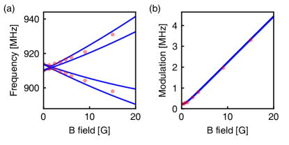
A Helmholtz coil positioned along the in-plane direction of sample D1 applies a small magnetic field. With this configuration the magnetic field is misaligned by with respect to three sites, which are therefore degenerate. Due to the lower concentration of defects oriented in-plane (Section I), significantly lower signal-to-noise ratio is expected for that site. As a result, we focus on the sites oriented to the field. Upon applying magnetic field, Zeeman splitting is observed, confirming the spin-dependent nature of these ODMR transitions [Fig. S5(a)]. The broadening of the lines at higher magnetic fields likely arises from a combination of inhomogeneity of the magnetic field for different sites and splitting of hyperfine transitions in the presence of an off-axis magnetic field.
A pronounced modulation of the spin echo decay is observed in our data [Fig. S5(b)]. The observed oscillation frequency increases with magnetic field, and arises from a set of hyperfine transitions being driven simultaneously in our experiment. To probe this further, we simulated the expected ODMR spectrum at low magnetic fields. Four transitions are present in total [Fig. S6(a)], but the separations are often smaller than the linewidths measured from CW ODMR. The four transitions at zero applied field can be labeled approximately as (from lowest to highest frequency)
| (1) |
| (2) |
| (3) |
| (4) |
where the triplet electronic spin levels are labeled by ,, and the nuclear spin levels are labeled by and . During the free precession time of spin echo sequence, extra phase accumulates between two nearby hyperfine levels owing to their energy difference. We simulate the effect of this extra phase accumulation on spin echo using the rotating frame Hamiltonian and find that the energy difference between the two levels and the modulation frequency are related by . By measuring the magnetic field dependence of the modulation frequency, we find consistent results between experiment and simulation shown in Fig. S6(b).
III.2 Spin Coherence Times () on Sample D1
The spin coherence time of SiV0 was previously characterized to be 1 ms below 20 K at X-band in sample D3, and was shown to be limited by spectral diffusion arising from the naturally abundant 13C bath. for sample D1 at X-band was extensively studied in Ref. Rose et al. (2018b). It was shown that for sample D1 is instead limited by instantaneous diffusion due to the high SiV0 concentration to be:
| (5) |
where ms is the spectral diffusion-limited and is the instantaneous diffusion-limited . The four orientations of SiV0 in D1 show preferential alignment with a population ratio of 1:1:3:3 D’Haenens-Johansson et al. (2011). The two out of plane sites have 3 times higher SiV0 concentration compared to the two in-plane sites with ms. For the higher (lower) concentration sites, was limited to 0.28 ms (0.48 ms).
In the low magnetic field regime where we performed ODMR measurements, we could not isolate a single site or a single spin transition. Since instantaneous diffusion is proportional to the spin density, a shorter (limited by greater instantaneous diffusion) is expected. Driving all four sites leads to a factor of 8/3 increase in SiV0 concentration. Another factor of 2 is expected from the fact that X-band measurements address a single nuclear spin level while at low field, we address both nuclear spin levels simultaneously. These two factors together lead to an instantaneous diffusion limited of ms and s. We note that differences in optical spin polarization and MW pulse fidelity between ODMR and X-band ESR are not considered in the estimation here, which could also affect the total spin density under MW driving.
III.3 Temperature Dependence of Spin Relaxation Times at Low Magnetic field
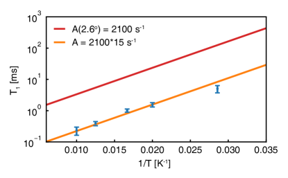
Spin relaxation times () are measured at different temperatures for the lower hyperfine transition at low magnetic field for sample D1. We note that temperature dependence of for SiV0 was previously studied using X-band ESR and can be described with an Orbach process Rose et al. (2018b)
| (6) |
where is the saturated at low temperature, is the activation energy for the Orbach process and is a prefactor that depends on the misalignment between the defect axis and the spin axis.
We find that the measured here is about 15 times shorter compared to the X-band measurement for sample D1 () and 105 times shorter compared to the X-band measurement for sample D3 () but still follows an exponential scaling with increasing temperature. The similar exponential dependence suggests that is likely also limited by Orbach process. The prefactor was shown to be strongly anisotropic due to different mixing rates between different spin states and phonon-activated Orbach excited state. Normally, when the magnetic field is aligned with the defect axis, no mixing of spin levels should occur so there shouldn’t be any magnetic field dependence of the anisotropy. However, for the 29Si enriched sample, we must also consider mixing of the Zeeman states due to the hyperfine interaction. At X-band, the transverse hyperfine interaction (79 MHz) is small compared to Zeeman splitting (9.5 GHz) so it can be ignored. At low magnetic field, the transverse hyperfine interaction is significant compared to the zero-field splitting (942 MHz) and non-negligable mixing occurs (Table I). For the lower hyperfine transition being measured here, we estimate using a Wigner rotation matrix that at zero field, the hyperfine interaction induced mixing is equivalent to a 5.0° rotation of the spin basis.
| Energy (MHz) | ||||||
| 980.15 | 1 | 0 | 0 | 0 | 0 | 0 |
| 980.15 | 0 | 0 | 0 | 0 | 0 | 1 |
| 907.28 | 0 | 0.998 | 0.061 | 0 | 0 | 0 |
| 907.28 | 0 | 0 | 0 | 0.061 | 0.998 | 0 |
| -3.43 | 0 | 0 | 0 | 0.998 | -0.061 | 0 |
| -3.43 | 0 | -0.061 | 0.998 | 0 | 0 | 0 |
We estimate the reduction in by calculating the ratio between and at the experimental misalignments using the parameters determined in Ref. Rose et al. (2018b). For the previous X-band measurements, and . This is consistent with the experimentally determined for sample D1 and for sample D3. For the misalignment caused by hyperfine interaction at zero-field, . This accounts for most of the observed reduction () in compared to a perfect misalignment.
By inspecting the eigenstates from Table I, the 980.15 MHz levels (which are involved in the higher hyperfine transition) are not mixed by the transverse hyperfine interaction: they remain pure states. The anisotropy of SiV0 was modeled by extracting a larger state overlap with the Orbach excited state Rose et al. (2018b). Therefore, we expect the higher hyperfine transition to have longer .
III.4 Temperature Dependence of ODMR Contrast
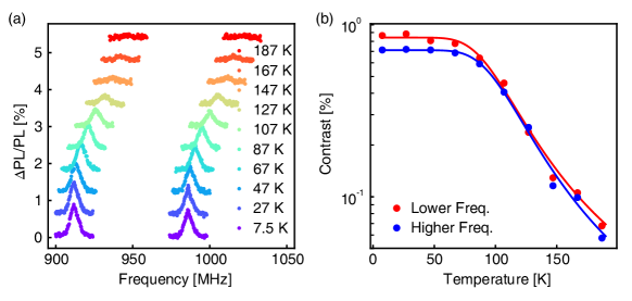
We measure the temperature dependence of continuous-wave ODMR spectra on sample D1 [Fig. S8(a)]. ODMR contrast is flat up to 70 K, and is still observable (about 0.07%) at 187 K. While the underlying physical process requires further detailed study, we fit the temperature dependence of contrast using a phenomenological model
| (7) |
where is the saturated contrast at low temperatures, A is an amplitude prefactor, T is the temperature, is the Boltzmann constant, and is the activation energy of a phonon-activated process. The fits yield an activation energy of meV for the lower hyperfine line, and meV for the higher hyperfine line. This temperature dependence differs from that of (16.8 meV activation energy), which suggests that shorter at higher temperature alone cannot explain the observed temperature dependence. Therefore, we suspect that additional phonon-induced spin mixing, and phonon-mediated non-radiative decay from the bound exciton excited states are responsible for the observed temperature dependence.
III.5 Power Dependence of ODMR Spectra
We measure the power dependence of continuous-wave ODMR spectra on sample D1. Upon lowering the microwave power, narrower linewidths are observed (Fig. S9). When the transition is not power broadened, we measure an inhomogeneous linewidth of MHz, which corresponds to an ensemble spin dephasing time of ns. The spin dephasing time extracted here matches with the result from Ramsey measurement.
IV Absorption measurements
V Saturation characteristics of optical spin polarization
We measure the time-dependent saturation characteristics of OSP on sample D2. Fig. S11(a) shows an OSP spectrum using constant pumping power and pumping time. The large difference in amplitude between the bound exciton (BE) transitions and off-resonant wavelengths demonstrates the wavelength selectivity of OSP for SiV0 centers. To further characterize the OSP, we measure the time-dependent saturation curves of OSP for several different wavelengths [Fig. S11(b)]. The ZPL wavelength (946.75 nm) is included for comparison. The initial spin population is scrambled using off-resonant excitation and a series of MW pulses to eliminate any residual polarization from previous interrogation [Fig. S1(c)]. Then, optical pulses with varying duration are applied to measure the saturation curve of OSP. The wavelengths are categorized into two groups: off-resonant (820 nm, 844 nm and 880 nm, open markers), and resonant (BE states: 855.5 nm and 886.5 nm and ZPL: 946.75 nm, filled markers). We fit the saturation curves with a bi-exponential function.
Interpretation of the observed timescales is complicated by the bulk nature of the experiment and the spectrally narrow excitation source, with contributions from far-from-saturation excitation dynamics, spin diffusion, and spin relaxation. However, some qualitative trends are clear; exciting at the ZPL reaches the highest value (62) but the saturation timescale is rather long. Exciting at the BE transition (855.5 nm), however, shows both high saturation (40) and a much shorter saturation timescale. OSP saturation with off-resonant excitation (844 nm and 880 nm) is slow, consistent with our lack of observation of ODMR when detuned from BE transitions [Fig. 4(a) in main text]. For 820 nm excitation above the ionization threshold Allers and Collins (1995), the saturated OSP is small (12) but the saturation time is fast, likely limited by ionization processes. Strikingly, saturated OSP for 886.5 nm shows a slow timescale but a high saturation value (59), suggesting high efficiency of OSP per optical cycle.
VI Spectral Decomposition of Optical Spin Polarization
Optical spin polarization is a measure of both absorption and spin polarization from all ground states. The ensemble optical linewidths in bulk samples are much larger than the spin splittings so optical excitation addresses many transitions involving all the spin levels. In order to disentangle the OSP from competing polarization processes, we develop a spectral decomposition method using a pump-probe scheme [Fig. S1(b)]. The OSP can be initialized with optical and microwave pulses as
| (8) |
where , and are populations of the three spin sublevels. The population of () is not involved because we are measuring spin echo using transition. A weak probe pulse then probes the net change in OSP
| (9) |
where is the population change of sublevel . We assume that the short-time spectrum will be proportional to the initial population of each spin sublevels () multiplied by their OSP spectra [, meaning net OSP change after a perfect initialization]. Under this assumption, the net OSP spectrum can be written as a superposition of OSP from all spin sublevels
| (10) |
This expression can be further simplified under specific selection rules as
| (11) |
where we have defined as probe induced population change of sublevel after a perfect initialization into sublevel and are weight factors depending on the selection rules.
Here, we consider two generic types of spin selection rules, assuming echo intensity between and is measured. For the first case, we consider no selection rules for optical excitation, meaning that and are treated equivalently. An excitation addressing will not lead to any observable effect since the depleted population from is distributed equally to and sublevels.
For the second case, we consider selection rules similar to magnetic dipole selection rules, where population transfer is only allowed from to and to . In this case, when measuring echo intensity between and , we expect because the depleted population in is not measured in the echo. We also expect because half of the depleted population from is transferred to which cannot be measured. The detailed derivation of is summarized in Table II.
| no selection rules | magnetic-dipole-like selection rules | |||||||
|---|---|---|---|---|---|---|---|---|
| selective excitation of | selective excitation of | |||||||
| -0.5 | -0.5 | - | - | |||||
| -0.5 | -0.5 | -0.5 | 0 | |||||
| -0.5 | -0.5 | -0.5 | 0 | |||||
| - | -1.5 | 1.5 | 0 | - | -1.5 | 2 | ||
| -1.5 | 1.5 | 0 | -1.5 | 2 | 1 | |||
Because we cannot fully map out the multiplicity and selection rules for these bound exciton states, we choose the first case (, and ) for data processing. The lack of selection rule is a more relaxed requirement since interactions in the excited states could give rise to spin mixing. We note that although choosing a specific set of over another would lead to differences in the relative amplitudes of , the resonance features and overall shapes of the spectra are still preserved.
Without any initialization, , meaning there is equal population in all three spin states. Ideally, the OSP from individual spin levels can be directly measured if . In reality, we achieve using our most efficient polarization wavelengths. Nevertheless, by initializing the spins differently, individual spectra can be decomposed. When the magnetic field is aligned to the defect axis, and are symmetric with respect to so we could assume and under initialization. This is consistent with the spectrum as the mirror image of spectrum, shown in Fig. S12. These simplifications lead to
| (12) |
By applying a pulse after the pumping pulse, the spin populations can be inverted
| (13) |
The OSP spectra and can then be decomposed from and using the measured initial populations and .
After decomposing the OSP spectrum for different spin states, OSP under arbitrary spin initialization can be reconstructed. To validate the effectiveness of our spectral decomposition, we apply MW pulses with different rotation angles (0, , and ) between the pump and probe pulses to achieve different spin initializations. We observe larger net OSP change into () using rotation (0 rotation) compared to rotation ( rotation), consistent with the difference in the spin initializations (Fig. S13, upper panel). Using the decomposed spectra and , we could also reconstruct the and spectra, which match well with the raw data using and rotations (Fig. S13, lower panel).
VII Isotopic Shifts of the Bound Exciton Transitions
According to the BE model, the pure electronic transition to the excited state is dipole forbidden so our level assignment for PLE in Fig. 3(a) starts from . However, we observe OSP resonances near 886 nm that have no correspondence to PLE and absorption peaks [Fig. 2(c)]. These transitions are tentatively assigned to the transitions. The states typically do not follow the Rydberg scaling due to the substantial central cell correction expected. Transition to the state is dipole forbidden so its observation in the OSP spectrum suggests the involvement of a phonon-related process. We find evidence of these phonon processes from the isotopic shift measured on different samples and ESR hyperfine lines. For transitions, we observe a 0.4 meV isotopic shift between 28Si and 29Si lines [Fig. S14(a)], consistent with the isotopic shift observed for the SiV- ZPL transition Dietrich et al. (2014). However, a larger isotopic shift of 0.7 meV is observed for the transitions [Fig. S14(b)] which suggests a different origin of isotopic shift.
VIII THEORETICAL DESCRIPTION OF BOUND EXCITON STATES OF SiV0
VIII.1 Effective Mass Description
The problem of describing (pseudo-) donor and acceptor defects in the solid state is discussed extensively in many textbooks Ashcroft and Mermin (1976); Cardona and Peter (2005). We revisit some key concepts here to clarify our description in the main text and outline our approach to simulations.
The simplest description of these systems is a hydrogenic model of the pseudo acceptor, where a positive charge is bound to a heavy central negative charge. The Hamiltonian here is thus Luttinger and Kohn (1955); Kittel and Mitchell (1954); Kohn and Luttinger (1955); Wu and Fisher (2008)
| (14) |
where is the effective mass of the exciton, and is the dielectric constant of the diamond host . This description neglects the spatial anisotropy imposed by the diamond lattice and the further lowering of symmetry from crystal-field effects introduced by the SiV0 defect. These effects are important and will be discussed below, but this simple model is useful for order-of-magnitude estimates.
The Schrödinger equation here can be solved as , where are the hydrogen-atom eigenstates and are their eigenenergies. The energies depend only on the principle quantum number, , so we may write
| (15) |
The Bohr radius of our artificial atom in diamond can be expressed as
| (16) |
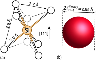
At the -point in diamond, three different effective masses are experimentally observed: ; ; Rauch (1962); Collins (1993). From Table III, we can see that the simplest hydrogenic approximation is poor for all states, and for the heavy hole state. The dimensions of the SiV0 point defect are on the order of a few Å, comparable to the spatial extent of these wavefunctions as shown in Fig. S15.
| n | (eV) | (eV) | (eV) | (Å) | (Å) | (Å) |
|---|---|---|---|---|---|---|
| 1 | 0.2930 | 0.8874 | 0.4437 | 4.31 | 1.42 | 2.85 |
| 2 | 0.0733 | 0.2219 | 0.1109 | 17.24 | 5.69 | 11.38 |
| 3 | 0.0326 | 0.0986 | 0.0493 | 38.78 | 12.81 | 25.61 |
| 4 | 0.0183 | 0.0555 | 0.0277 | 68.94 | 22.76 | 45.53 |
| 0 | 0 | 0 |
Several features of the experimentally observed transitions are in good agreement with this description. From Fig. 3 of the main text, we extract values of
| (17) |
The ionization threshold is in good agreement with previous photoconductivity measurements, and the effective Rydberg energy is in the range predicted by the light and split-off effective masses (0.293 eV and 0.444 eV, respectively). The data in Fig. 3(b) also shows that the level significantly deviates from the model of a simple hydrogenic series, as expected.
To gain further insight into these states, we go beyond a simple hydrogenic model and explicitly consider the effects of spin-orbit coupling and the crystal field. Parameters which cannot be determined from experimental data in the main text are calculated by DFT, as described in Section IX.
VIII.2 Effective Hamiltonian For ()
The -point of the valence band in diamond is triply degenerate and splits into the light-hole band, heavy-hole band and split-off band parabolic edges. In order to interpret the character of the weakly bound hole, we assume that the hole wavefunction is similar to that of the -point (). However, it is confined to the envelope function taken from the hydrogenic model (), yielding
| (18) |
For , is a totally symmetric orbital that transforms as the representation of the local symmetry. The wavefunction at the -point in pristine diamond is triply degenerate, which becomes due to the “crystal-field” induced by the SiV0 defect. The index is for and for the orbital. The total wavefunction transforms as the product of the two constituent wavefunctions, . In other words, inherits the threefold multiplicity of the valence band maximum (VBM) states. The following effective Hamiltonian describes this orbitally three-dimensional hole system,
| (19) |
where “CF” and “SO” are the crystal field and spin-orbit terms, respectively, and and are the strength of crystal-field and spin-orbit interactions. If we choose the quantization axis along the [111] direction, parallel with the symmetry axis of the SiV0 defect, then we may express the operators in Eq. (19) as
| (20) |
The crystal field lifts the degeneracy of the states and ; (). The three orbitals can be treated as an system, where the quantum number labels the eigenstates of the -point as , or in the matrix representation as and .
Now we consider the effect of the spin-orbit interaction. We assume that the weakly bound hole is almost spherically symmetric, therefore is also spherically symmetric, thus it can be described by a single value. The parameter can be connected with the spin-orbit splitting of the VBM of diamond: .
The experimental value of the spin-orbit splitting of diamond is Rauch (1962); Herman et al. (1963); Serrano et al. (1999). Ab initio calculations tend to overestimate this value by a factor of two ( Herman et al. (1963); Serrano et al. (1999); Willatzen et al. (1994)), consistent with our ab initio DFT calculations yielding . We calculated this value on a -point centered k-point set for a diamond primitive cell, which results in . The factor of two between the experimental data and calculated value might indicate the uncertainty in our DFT method or may represent a subtlety in the interpretation of the 6 meV signatures in the spectrum for , as noted in an earlier study Serrano et al. (1999). Nevertheless, we cannot unambiguously determine the source of this discrepancy and this issue is beyond the scope of the present manuscript.
We used the following parameters to construct our model directly taken from DFT calculations. According to ab initio SCF Gali et al. (2009) results, the hole experiences crystal field [see Sec. IX.3 and Fig. S17(b)]. The spin-orbit energy is estimated from DFT calculations on the SiV- defect and is obtained (Fig. S18). The results of the direct diagonalization of this effective Hamiltonian are listed in Table IV.
| energy (meV) | L | S | J | ||||||
|---|---|---|---|---|---|---|---|---|---|
| split-off band | -10.802 | 1 | 0.5 | 0.57 | 0.5 | 0.85 | -0.35 | -0.43 | |
| -10.802 | 1 | 0.5 | 0.57 | -0.5 | -0.85 | 0.35 | -0.43 | ||
| heavy-hole band | 2.007 | 1 | 0.5 | 1.50 | 1.5 | 1 | 0.50 | 0.50 | |
| 2.007 | 1 | 0.5 | 1.50 | -1.5 | -1 | -0.50 | 0.50 | ||
| light-hole band | 8.795 | 1 | 0.5 | 1.46 | 0.5 | 0.15 | 0.35 | -0.07 | |
| 8.795 | 1 | 0.5 | 1.46 | -0.5 | -0.15 | -0.35 | -0.07 |
We calculate a 9 meV splitting between the quasi-particle hole levels. The experimentally-observed splitting between the two spin polarization resonances is 5.86 meV (difference between 886 nm and 889 nm peaks in the spectrum), which is consistent with the experimental value of the spin-orbit parameter. The discrepancy between our calculation and experimentally observed values is consistent with the general observation that ab initio methods appear to overestimate this value.
We have so far only considered the wavefunction of the hole. The resulting SiV- defect also has non-zero spin, and can be described by a second hole localized on the defect. This second hole may be described as a orbitally degenerate spin-half system that splits into the Kramers doublets. Under the assumption that the two holes are independent of each other, we can construct the two-hole wavefunction as a direct product of the localized hole in the SiV- orbital and the weakly-bound hole as follows:
| (21) |
| (22) |
| (23) |
One finds from Eqs. (21-23) that the split-off hole, the heavy hole, and the light hole Kramers doublets will split further due to the coupling of the additional hole. Note, the representations are double group representations.
| triplets | |||||
|---|---|---|---|---|---|
| singlets | |||||
| energy (meV) | |||||
| split-off band | -10.948 | 0.44 | 0.42 | 0.15 | |
| -10.948 | 0.44 | 0.42 | 0.15 | ||
| -10.948 | 0.44 | 0.42 | 0.15 | ||
| -10.948 | 0.44 | 0.42 | 0.15 | ||
| -10.853 | 0.15 | 0 | 0.85 | ||
| -10.853 | 0.15 | 0 | 0.85 | ||
| -10.802 | 0 | 0.15 | 0.85 | ||
| -10.802 | 0 | 0.15 | 0.85 | ||
| heavy-hole band | 1.838 | 0.49 | 0.51 | 0 | |
| 1.838 | 0.49 | 0.51 | 0 | ||
| 1.838 | 0.49 | 0.51 | 0 | ||
| 1.838 | 0.49 | 0.51 | 0 | ||
| 2.007 | 0 | 0 | 1 | ||
| 2.007 | 0 | 0 | 1 | ||
| 2.007 | 0 | 0 | 1 | ||
| 2.007 | 0 | 0 | 1 | ||
| light-hole band | 8.506 | 0.85 | 0 | 0.15 | |
| 8.506 | 0.85 | 0 | 0.15 | ||
| 8.770 | 0.07 | 0.08 | 0.85 | ||
| 8.770 | 0.07 | 0.08 | 0.85 | ||
| 8.770 | 0.07 | 0.08 | 0.85 | ||
| 8.770 | 0.07 | 0.08 | 0.85 | ||
| 8.795 | 0 | 0.85 | 0.15 | ||
| 8.795 | 0 | 0.85 | 0.15 | ||
We note that both singlet and triplet spin configurations appear in these two-hole wavefunctions. The energy levels of these states cannot be predicted by this simple model and we approximate those by ab initio simulations. We again rely on the SCF method. We can impose a triplet coupling between the localized hole and the weakly bound hole, thus their spin state is maximally polarized . However, we can also determine when the two holes exhibit different spin projections such as which mimics the singlet configuration.

In this way, we are able to determine the difference between the singlet and triplet states as meV, see Sec. IX.5 for details. Our DFT results follow Hund’s rule in that the triplet configuration is lower in energy than the singlet configuration. Thus our effective Hamiltonian now becomes
| (24) |
where the singlet operator raises the energy of the singlet states as while leaving the three triplet projections untouched. Considering the two-hole wavefunction significantly increases the dimensionality of the problem, as can be seen from Table V. However, the coupling of the second hole only perturbatively splits the three levels by 0.2 meV. Thus the single hole picture from Table IV is representative of the physical nature of the system.
VIII.3 Extension to the Bound Excitons
The computational complexity of the system increases rapidly with , thus our calculations for the transitions in Sec. IX.7 are only a crude approximation. However, we can use the physical intuition we developed for the states to describe some properties of these states. We summarize the energy levels of the bound exciton states in Fig. S16.
For example, at , four different envelope functions are possible with . There is a “2s” hole with and that transforms as . There is also a 3-fold degenerate “2p” solution, which under the crystal field splits into with representation and (,) with representation. These states are visually depicted in Fig. S16.
We make the following observations regarding the manifolds:
-
•
If the primary source of the spin-orbit splitting again comes from the wavefunction at the -point then the spin-orbit interaction for levels will be similar to the value, approximately meV. In this case, this splitting would be independent of since the wavefunction will be the same for all .
-
•
Only transitions to states with -like envelope functions are expected to be optically active. Clusters of four peaks are observed experimentally for “2p” and “3p”, see Fig. 3(a) of the main text.
-
•
The energies of “1s”, “2s” peaks deviate most significantly from the Bohr model Eq. (17) [Fig. 3(b)]. However the “2p” and “3p” states largely follow the law of the Bohr model. We treat this difference as a central cell correction which alters the energy level of the “1s” state significantly (see Sec. IX.7 for details). The localized orbital of the SiV- excludes the from the 6 first neighbor carbon atoms, where it would exhibit otherwise the highest probability density, increasing the spatial extent of this wavefunction. This central cell correction effectively increases the excitation energy of “1s” and “2s”, but leaves “2p” and “3p” intact due to the radial node at the origin in their probability density.
-
•
It is extremely complicated to setup an effective Hamiltonian for “2p” and “3p” states in a similar fashion as we did for “1s” in Eq. (19). Not only would the wavefunction at the -point would carry the orbital momentum of , but the envelope function of “p” orbitals would also exhibit an angular momentum. However, the “2s” should behave very similarly to “1s”, albeit with altered crystal-field and spin-orbit parameters.
IX Results of DFT calculations for the energy levels of Bound Exciton resonances
IX.1 Method Summary
First principles plane-wave supercell DFT calculations are used to study the SiV0 center in diamond as implemented in the vasp code Kresse and Furthmüller (1996). The excited states are considered by the SCF method which involves electron-hole interaction and relaxation of ions upon excitation Gali et al. (2009). The paramagnetic states are treated by spin polarized functionals. The spin-orbit energies are calculated within the scalar relativistic approximation Steiner et al. (2016). The usual projector augmented wave (PAW) projectors Blöchl (1994); Bengone et al. (2000) are applied on the carbon and silicon atoms with a plane wave cutoff of 420 eV. We provide a foundation for the accurate calculation of the effective mass (acceptor) states within supercell modeling in the subsequent sections. Our approach requires scaling of the properties as a function of supercell size. In the scaling procedure, supercells of up to 8000 atoms are applied within the semilocal Perdew-Burke-Ernzerhof (PBE) DFT functional Perdew et al. (1996), whereas supercells of up to 1000 atoms are employed in the hybrid Heyd-Scuseria-Ernzerhof (HSE) DFT functional Heyd et al. (2003); Krukau et al. (2006).
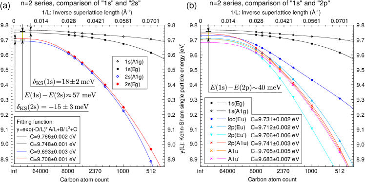
IX.2 Determining the , Parameter From Kohn-Sham Levels
We calculate the electronic structure of an SiV- defect embedded in diamond cubic supercells of 64, 216, 512, 1000, 1728, 2744, 4096, 5832, and 8000 carbon atoms within -point sampling of the Brillouin-zone without incorporating the spin-orbit interaction by means of the PBE Perdew et al. (1996) DFT functional. In this case, the VBM at the -point should be triply-degenerate in the perfect supercell calculation. However, due to the presence of the crystal field induced by the defect in the defective supercell, the cubic symmetry of the supercell is lowered to , thus the VBM at the -point splits into and states. We define the Kohn-Sham energy difference of these two as . The optical excitation process can be described as promotion of an electron from the delocalized or levels to the unoccupied and localized level in the same spin channel. We use spin majority (minority) channel to refer to the appropriate Kohn-Sham level in the calculation. As an example, for a spin system in the configuration, the spin-up electrons are in the majority, whereas in the configuration the situation is reversed.
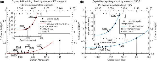
Table VI lists the Kohn-Sham energies of the VB states and the localized and orbitals for the excitation process of SiV0 that occurs at 946 nm (taking the relaxation of ions upon excitation into account). We note that the in-gap localized level is occupied only by one electron, so we put half-half electrons onto and states, in order to average out the Jahn-Teller instability of state of SiV-.
| C atom count | 64 | 216 | 512 | 1000 | 1728 | 2744 | 4096 | 5832 | 8000 | ||
| lattice constant | Å | 7.13 | 10.70 | 14.26 | 17.84 | 21.40 | 24.97 | 28.54 | 32.10 | 35.67 | |
| localized | eV | 8.810 | 9.389 | 9.308 | 9.432 | 9.516 | 9.575 | 9.616 | 9.646 | 9.668 | |
| eV | 8.810 | 9.389 | 9.308 | 9.432 | 9.516 | 9.575 | 9.616 | 9.646 | 9.668 | ||
| delocalized | eV | 8.894 | 9.710 | 9.615 | 9.675 | 9.702 | 9.716 | 9.725 | 9.730 | 9.735 | |
| eV | 8.894 | 9.710 | 9.616 | 9.675 | 9.702 | 9.716 | 9.725 | 9.730 | 9.735 | ||
| delocalized | eV | 9.500 | 9.931 | 9.705 | 9.724 | 9.733 | 9.740 | 9.745 | 9.749 | 9.754 | |
| localized | eV | 11.082 | 11.090 | 10.831 | 10.886 | 10.934 | 10.975 | 11.007 | 11.033 | 11.055 | |
| eV | 11.082 | 11.090 | 10.831 | 10.886 | 10.934 | 10.975 | 11.007 | 11.033 | 11.055 | ||
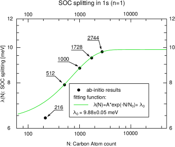
| meV | 605.3 | 221.5 | 89.7 | 48.6 | 31.1 | 24.5 | 20.3 | 19.1 | 18.8 | 18.50.2 | |
| meV | 757.6 | 247.4 | 102.4 | 55.0 | 35.9 | 27.1 | 20.8 | 18.5 | 7.91 |
Fig. S17(a) shows the crystal-field parameter as calculated from the energy gap of the Kohn-Sham levels. In order to scale the result to the infinite system (isolated defect), we fit an function to the data ranging in size from 216-atom to 8000-atom supercells. The Kohn-Sham energies, however, are auxiliary quantities in Kohn-Sham DFT, thus we move to the next task of calculating the total energy differences by means of SCF method.
IX.3 , Parameter From SCF calculations
To take into account the electron-hole interaction, we calculate the total energies by SCF method at the PBE level, where we leave and constrain a hole inside a VBM state, and then converge the electronic structure with this constraint. We calculate the total energy of the SiV- plus a hole left behind in the delocalized state, and also where the hole left behind is in the delocalized state. The calculated SCF energies are scaled by a fit function [Fig. S17(b)]. The fit describes the crystal field from total energy differences [] as a function of supercell sizes ranging from 64-atom to 8000-atom supercells. The fit yields meV.
IX.4 Spin-Orbit Coupling at the -Point
Calculations of the spin-orbit coupling are performed as described previously Thiering and Gali (2018). We calculate the ground state of SiV- and determine the spin-orbit splitting of the delocalized level in the -point at the VBM. We can determine the spin-orbit splitting as the energy difference between and levels. We find that the accurate calculation of this property requires scaling of supercell sizes as shown in Fig. S18, where we fit an exponential scaling function to achieve the isolated defect limit with an infinitely large supercell. The 216-atom supercell is too small for this quantity within -point approximation and is not taken into account in the fitting procedure.
IX.5 Triplet-Singlet Splitting of the Series
We determined the strength of triplet-singlet splitting from the single particle Kohn-Sham levels of SiV- center. Table VI shows the spin minority () channel, where the optical transition occurs (one electron fills the double degenerate in the ground state which is fully occupied in the excited state). Table VII lists the Kohn-Sham levels in the spin majority channel, where the is fully occupied by two electrons. While the transitions from any occupied single electron orbital from the spin minority channel are spin allowed upon optical excitation, the excitation process which flips the spin is forbidden (because of the relatively small spin-orbit interaction). Therefore the energy splitting for the same orbitals but with the opposite spin channel provides insight into the spin forbidden transition. That is, gives a tentative approximation for the energy difference when the “1s” hole couples with the with a spin triplet or spin singlet wavefunction. We note that the “1s” exhibits different triplet-singlet splitting (). However, we use only the definition of to derive the full singlet manifold, see Eq. (24).
| C atom count | 64 | 216 | 512 | 1000 | 1728 | 2744 | 4096 | 5832 | 8000 | ||
| -localized | eV | 8.726 | 9.261 | 9.219 | 9.377 | 9.482 | 9.553 | 9.601 | 9.634 | 9.659 | |
| eV | 8.726 | 9.261 | 9.219 | 9.377 | 9.482 | 9.553 | 9.601 | 9.634 | 9.659 | ||
| -delocalized | eV | 8.731 | 9.671 | 9.599 | 9.667 | 9.697 | 9.712 | 9.722 | 9.728 | 9.733 | |
| eV | 8.731 | 9.671 | 9.599 | 9.667 | 9.697 | 9.712 | 9.722 | 9.728 | 9.733 | ||
| -delocalized | eV | 9.490 | 9.928 | 9.704 | 9.723 | 9.732 | 9.740 | 9.744 | 9.749 | 9.753 | |
| -localized | eV | 10.884 | 10.880 | 10.599 | 10.644 | 10.689 | 10.729 | 10.760 | 10.785 | 10.807 | |
| eV | 10.884 | 10.880 | 10.599 | 10.644 | 10.689 | 10.729 | 10.760 | 10.785 | 10.807 | ||
| meV | 758.7 | 257.4 | 105.0 | 56.0 | 35.4 | 27.4 | 22.4 | 20.8 | 18.2 | 18.50.2 | |
| meV | 9.92 | 3.45 | 1.65 | 0.99 | 0.71 | 0.59 | 0.50 | 0.53 | 0.54 | 0.340.01 | |
| meV | 163.36 | 39.31 | 16.86 | 8.37 | 4.97 | 3.40 | 2.60 | 2.19 | 1.97 | 0.490.13 |
IX.6 Determining the Excitation Energy by Means of SCF Calculation at the HSE06 Level
Although the PBE functional provides insight into the nature of the bound exciton states, it underestimates the optical excitation energies. To enable quantitative comparison to experimental data, we determine the optical excitation energies by means of the HSE06 functional Heyd et al. (2003); Krukau et al. (2006), which provides approximately eV accuracy for the excitation and ionization energies of point defects in diamond. However, supercells containing more than 1000 carbon atoms are computationally too expensive using the HSE06 functional. Thus, we exploit the two functionals for two different purposes: the PBE functional is used to simulate the supercell size dependence of these properties at the limit, i.e., completely isolated defect limit, and the HSE06 functional is used to correct the optical excitation energies by comparing the PBE and HSE06 results at smaller supercells. We summarize the optical excitation processes in Fig. S19 and Table VIII, where we depict three excitation processes:
- •
-
•
Excitation from the localized orbital into the bound exciton state: .
-
•
Excitation from the localized orbital into the bound exciton state: . This is the acceptor adiabatic charge transition level.
| BE excitation | charge transition level () | |||||||
|---|---|---|---|---|---|---|---|---|
| 64 | 0.140 | 1.972 | 1.943 | 1.445 | 1.573 | 1.616 | 1.293 | 1.741 |
| 216 | 0.093 | 1.489 | 1.459 | 1.019 | 1.234 | 1.276 | 0.975 | 1.309 |
| 512 | 0.070 | 1.374 | 1.344 | 0.946 | 1.224 | 1.267 | 0.929 | 1.259 |
| 1000 | 0.056 | 1.328 | 1.298 | 0.943 | 1.256 | 1.298 | 0.937 | 1.276 |
| 1728 | 0.047 | 0.953 | 0.952 | |||||
| 2744 | 0.040 | 0.966 | 0.971 | |||||
| 4096 | 0.035 | 0.977 | 0.985 | |||||
| 5832 | 0.031 | 0.986 | 0.997 | |||||
| 8000 | 0.028 | |||||||
| 0 | 1.297 | 1.268 | 1.034 | 1.437 | 1.480 | 1.121 | 1.547 | |
| exp. | 1.311 | 1.393 | 1.53 | |||||
IX.6.1 Excitation between the localized states
We determined the excitation process in various supercell sizes between carbon atoms by means of HSE06 functional. The excitation process that corresponds to the zero-phonon line optical signals at 946 and 951 nm can be expressed by the following formula:
| (25) |
Here, is the total energy of the SiV0 center in its ground state in a supercell with lattice constant . The second term depicts the total energy of the excited state. We showed in a previous study Thiering and Gali (2019) that the product Jahn-Teller effect plays a significant role in the excitation process of SiV0. Thus, we correct the pure electronic ab initio data by the following 29.7 meV correction,
| (26) |
where eV is the product Jahn-Teller ground state in the 512-atom diamond supercell and eV is the value as obtained from Eq. (25). Here, we assume that the correction from the product Jahn-Teller effect does not depend on the size of the supercell.
IX.6.2 transition, charge transition level
Determining correct charge transition levels of defects always has been a difficult task in the supercell method. The origin of the inaccuracy is the Coulomb interaction which converges to zero with a long range strength. In a supercell that embeds a charged point defect, the mirror images of the charged defect and the compensating jellium charge in the plane wave supercell model interact via the long range Coulomb interaction. There are various correction schemes developed over the years to correct this artificial interaction such as Makov and Payne Makov and Payne (1995) (MP), Freysoldt, Neugebauer, and Van de Walle Freysoldt et al. (2009) (FNV), and Lany and Zunger Lany and Zunger (2008) (LZ). However, while the correction schemes provide accurate charge transition levels for supercells for a given size for moderately localized defect states, the most reliable method is to calculate the charge transition level with various supercells and fit the strength of the Coulomb interaction. Thus we determined the charge transition energy as follows
| (27) |
which consists of three individual DFT calculations. The first term is the total energy of the SiV- defect. The second is the total energy of the SiV0 defect. The third is the valence band maximum of the perfect supercell. This is the Kohn-Sham eigenvalue of the highest occupied band of the diamond supercell with lattice size, where the Brillouin zone is sampled only at the -point. We fit the following curve to our data to approach the bulk limit Komsa et al. (2012):
| (28) |
The term is the long range monopole term of Coulomb interaction, the second is the quadrupole term, while we seek the value of corresponding to the isolated defect limit. We fit this formula to our ab initio data by means of HSE06 and PBE DFT functionals. The results are depicted in Fig. S19(a). HSE06 provides 1.55 eV which is in excellent agreement with the experimental data (1.53 eV).
IX.6.3 Screening Effects in the Transition
The localized excitation can be considered as a two-particle system. The first particle in SiV- traps a positively charged hole. We study an analogous system with a hydrogen atom confined into a small supercell. There the positively charged proton attracts the negative electron. When viewed from a remote distance, both systems are localized and neutral. If the supercell size is much larger than the Bohr radius of the hydrogen atom-like system () or radius for SiV defect (see Table III), then the effect of the charged central particle is screened. This screening effect can have non-trivial effects on the functional form of the calculated energy as the supercell size is varied.
First, we determine the ratio of the screening length () versus the Bohr radius of hydrogen (). Then, we use this ratio to approximate the screening length for the bound exciton excitation. We note that this screening effect does not happen for the case as the VBM electron is delocalized all over the diamond lattice.
It can be observed in Fig. 3(b) that the state is poorly described by the simple model. The origin of this correction is that the orbital is expelled from the central region of the defect as the orbital of SiV- already occupies this region. Therefore, the binding energy will be increased by eV, and the effective radius () will be larger than that of the simple Bohr model (). However we also take into account that the 1s orbital is active by an ungerade phonon. Therefore the real central cell correction is only . Here we determine this effective radius for the case. We search for the effective that reproduces the excitation-energy () by means of central cell correction as given by
| (29) |
where is the ionization energy. Thus the effective Bohr radius is more than twice as large as the simple hydrogen model would indicate for the state,
| (30) |
We also determine the ratio of the screening length () to the Bohr radius (). We model this with a hydrogen atom in the simple cubic supercell with lattice constants (). Since this system contains a single electron we apply the exact Hartree-Fock method in the calculation with a soft PAW potential with a plane wave cutoff of 200 eV. The results are shown in Fig. S19(d). One can clearly see that the Coulombic scaling () deviates at sufficiently large supercells. We note that this scaling behavior is independent of the choice of the ionic potential of the proton (not shown) and the calculated total energies have a constant shift in each supercell. From a sufficiently far vantage point, the hydrogen atom is a neutral object, thus at large supercells ( Å), the energy of the system converges exponentially to a constant energy. We fit the total energies by
| (31) |
where the Coulomb interaction () is screened by . We note that the repulsive term is missing because only a single proton appears in the system. Using this fitting procedure, we find . The screening radius for the periodic array of hydrogen atoms is 3.56 times larger than the Bohr radius ( ) of the isolated free hydrogen atom.
Combining these results gives
| (32) |
As a consequence, the effective screening lengths based on theoretical considerations and the hydrogen atom model for heavy hole, split-off hole, light hole, respectively, are the following:
| (33a) | |||
| (33b) | |||
| (33c) |
which approaches as obtained from the fit to ab initio data. Therefore, we can rationalize and explain the existence and magnitude of the screening length. This highlights again that the hydrogen-model for the bound exciton excited state is a poor approximation. The accuracy of this model is greatly improved for excited states.
IX.6.4 Bound Exciton Transition
We determine the excitation energy to the lowest bound exciton state with the following formula,
| (34) |
which is very similar to Eq. (25) except that we have replaced the excited state with . Upon inspection of the and results, both cases exhibits the long range Coulomb scaling. However, the analysis in the previous section shows that the Coulomb interaction is screened for the state. From a sufficiently large distance, the SiV- center plus a bound hole is a neutral object. Therefore at the scaling should be overtaken by a fast converging function such as screening damped by an exponential function. Thus we used the following fit function for the bound exciton resonances,
| (35) |
We determine the screening length from PBE results (), where are fit parameters. Next, we use the fitted D to constrain HSE06 results, thus we assume that the is fixed, and allowed the remaining parameters to fit our data. Additionally we need to take into account that the state is optically not allowed by itself since it can be only observed by coupling to the localized vibration mode of the Si atom. Therefore one has to add the frequency (energy) of this oscillatory motion meV (see Table I in Ref. Londero et al. (2018)) to the excitation energy which results in
| (36) |
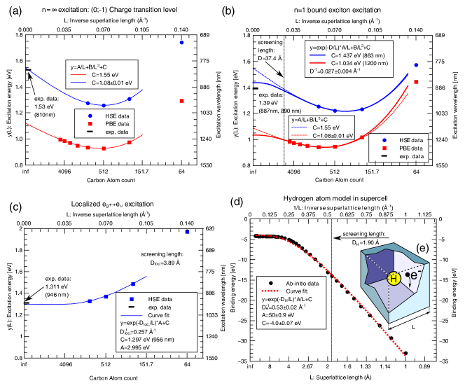
IX.7 Central Cell Correction and Transitions
We could also tentatively converge some of the resonances in the DFT calculations. We are unable to calculate these states by means of the accurate, but computationally-demanding, SCF calculations. Nevertheless, Kohn-Sham orbitals and levels of SiV- provide additional information beyond the “1s” states. We plot energies (not shown in Table VI) below the localized orbital in Fig. S20. The “2s” excitation splits into in a similar manner as the “1s”. The energy separation between them is approximately meV, much larger than the separation between the “2p” and “1s” series, meV. We note that the “2s” orbitals do not mix with the state because of the different parity of the wavefunctions but the “2p” orbitals can in principle mix with the state, making an accurate calculation demanding.
There are three times as many “2p” than “2s” states, , because there are three 2p orbitals (, , ), in addition to three orbitals split from the VBM states. According to ab initio calculations, we can assign a set of and orbitals for the series in Fig. S20(b) but cannot find the two orbitals. We suspect that the 8000-atom supercell is still too small to accommodate these states, thus our predictions about “2p” states can only be tentatively compared to the experimental data.
Nevertheless, our results clearly indicate that the “1s” is followed by the “2p” and not by the “2s”. This is not a surprising result in the light of the fact that the “1s”, “2s” orbitals are totally symmetric and have maximum density of their wavefunctions at the core of the SiV- defect, making them subject to a more significant central-cell correction.
If we compare this result against the experimental spin polarization and optical absorption spectra then one can tentatively assign the spin-polarization peaks, which are not optically active at 837 nm [see Fig. 3(a)], to the “2s” bound exciton resonance. Finally, we note that we cannot fully exclude the possibility that “3d” orbitals can also play a role in the optical spin polarization with photo-excitation near 830-840 nm wavelength region in the spin polarization spectra.