Valley-Current Splitter in Minimally Twisted Bilayer Graphene
Abstract
We study the electronic transport properties at the intersection of three topological zero-lines as the elementary current partition node that arises in minimally twisted bilayer graphene. Unlike the partition laws of two intersecting zero-lines, we find that (i) the incoming current can be partitioned into both left-right adjacent topological channels and that (ii) the forward-propagating current is nonzero. By tuning the Fermi energy from the charge-neutrality point to a band edge, the currents partitioned into the three outgoing channels become nearly equal. Moreover, we find that current partition node can be designed as a perfect valley filter and energy splitter controlled by electric gating. By changing the relative electric field magnitude, the intersection of three topological zero-lines can transform smoothly into a single zero line, and the current partition can be controlled precisely. We explore the available methods for modulating this device systematically by changing the Fermi energy, the energy gap size, and the size of central gapless region. The current partition is also influenced by magnetic fields and the system size. Our results provide a microscopic depiction of the electronic transport properties around a unit cell of minimally twisted bilayer graphene and have far-reaching implications in the design of electron-beam splitters and interferometer devices.
Introduction—. The triangular networks of topologically confined states in graphene-based moiré patterns, which arise naturally in minimally twisted bilayer graphene (t-BG) networkSTM2018 ; networkscience2018 ; networkAline2018 ; prbnetwork2018 ; networls-multi ; network2013 ; science12 ; nethelin ; networkwk ; magneticfieldwk ; sciencejun ; PNAS and graphene/hexagonal boron nitride (h-BN) superlattices pressure ; GrBN , have attracted much attention networkSTM2018 ; networkscience2018 ; networkAline2018 ; prbnetwork2018 ; networls-multi ; network2013 ; science12 ; nethelin ; networkwk . The presence of a minimally twist changes the local stacking order, arranging the AB/BA stacking regions periodically in space. The perpendicular electric field in t-BG or the sublattice potential difference in a graphene/h-BN bilayer leads to an energy gap that results in opposite valley Chern numbers at the AB/BA stacking regions. At the interfaces between different topological regions, topologically confined states (i.e., zero-line modes; ZLMs) appear and form networks zlm ; zlm1 ; folded ; partition ; kink ; 2013 ; 2015 ; 2016 ; NP ; N2015 ; Natphys . Recently, a network of topologically protected helical states was imaged in a minimally t-BG through scanning tunneling microscopy networkSTM2018 ; nethelin , and optical techniques science12 . Because of the three-fold rotational symmetry of the lattices, the elementary component of this network is the intersection of three ZLMs. However, the microscopic electronic transport properties of this intersecting point remains poorly understood.
In this Letter, we study the transport properties of three intersecting ZLMs connected to six terminals. When current is injected from one terminal, we find notable partitioning towards the forward channel, this situation is qualitatively different to the intersection of two ZLMs, where no forward propagation of current is observed. In the case of three intersecting ZLMs, the incoming current is partitioned towards the forward and the two adjacent zero-lines. This current partitioning depends strongly on the size of the central region when the region is small but saturates when it is large. By tuning the Fermi level, we find that the current partition can be controlled over a wide range. A perpendicular magnetic field can tune the currents propagating to the adjacent lines whereas the forward-propagating current remains quite robust. By changing the size of the AA stacking zone, we also study the effect of a twist angle on the transport properties. We find that (i) our device can support stable current partitioning even without a perpendicular electric field and (ii) the electric field allows to tune the partition properties and turn the device into a valley-current splitter.
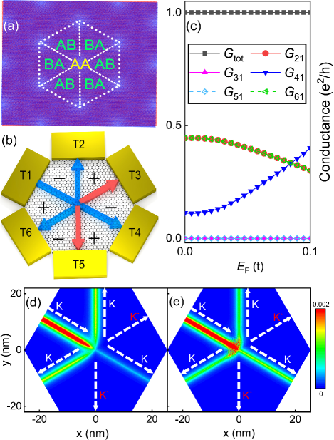
Model Hamiltonian—. The general stacking order of the moiré pattern is shown in Fig. 1(a), where the bright zone in the center corresponds to AA stacking. The size of AA stacking region decrease with the decreasing of the twist angle. Around this central zone, alternating periodic chiral AB or BA stacking regions are formed. At the interfaces between the AB and BA stacking regions, domain walls appear, indicated by the white dashed lines. By applying a perpendicular electric field, the centers of the chiral stacking regions become gapped while gapless ZLMs form at the domain walls networkSTM2018 ; nethelin ; science12 . The AA stacking zone is located at the intersection of three concurrent ZLMs, which are successively rotated by . Without loss of generality, in our calculations we consider a monolayer graphene flake with position-dependent staggered sublattice potentials to form six adjacent regions with different valley Hall topologies labeled by signs in Fig. 1(b), that correspond to AB/BA stacking regions under an electric field in a twisted bilayer graphene. The valley Hall domain walls form three intersecting zero-lines while the intersection region corresponding to the AA stacking zone in the moiré pattern of a twisted bilayer is not gapped locally. The monolayer graphene flake with staggered site potentials can be described by the following -orbital tight-binding Hamiltonian
where is a creation (annihilation) operator for an electron at site , and eV is the nearest-neighbor hopping amplitude. The sublattice potentials are spatially varying, with == in regions labeled by as shown in Fig. 1(b), where 2 measures the magnitude of the staggered sublattice potential difference.
The zero-lines are connected to six reservoirs labeled Ti (–) as shown in Fig. 1(b). Herein, we take T1 to be the injection terminal. The electronic transport calculations are based on the Landauer–Büttiker formula Datta and recursively constructed Green’s functions wang . The conductance from -terminal to -terminal is evaluated from
where is the retarded/advanced Green’s function of the central scattering region, and is the line-width function describing the coupling between -terminal and the central scattering region. The propagation of a ZLM coming in from -terminal is illustrated by the local density of states at energy , which can be calculated by
where is the actual spatial coordinate.
Current Partition Laws—. In our calculations, the central region is a hexagon with circumcircle diameter nm, and the diameter of AA stacking zone is nm unless stated otherwise. With , we calculate how the current partition depends on the Fermi energy as shown in Fig. 1(c). The current partition laws can be summarized as:
| (1) | |||
| (2) | |||
| (3) |
Here, Eq. (1) restricts current partitioning into zero-lines with opposite chirality, while the condition in Eq. (2) requires the mirror reflection symmetry of the partition, that is broken in the presence of a magnetic field as we show later. Equation (3) implies that there is no backscattering due to inter-valley scattering, and indeed any reflected current remains very weak even in the presence of disorders zlm .
Note that the forward-propagating conductance is nonzero because the zero-line from T1 to T4 has the same chirality, in contrast to the case of two intersecting zero-lines where the forward propagation is forbidden by the chirality conservation rule. Moreover, the forward-current transmission strongly depends on as shown in Fig. 1(c). When is close to the charge-neutrality point (CNP), is less than the conductance of towards the sides. When is shifted away from the CNP and moves toward the bulk band edges, increases gradually and exceeds when . The current partition at different is shown more clearly in Figs. 1(d) and (e), wherein the local density of states for current injected from T1 is plotted at and , respectively. This Fermi-energy dependent current partition suggests that longitudinal transport may be greatly modified through a perpendicular electric gate by altering the current percolation properties through multiple partition nodes.
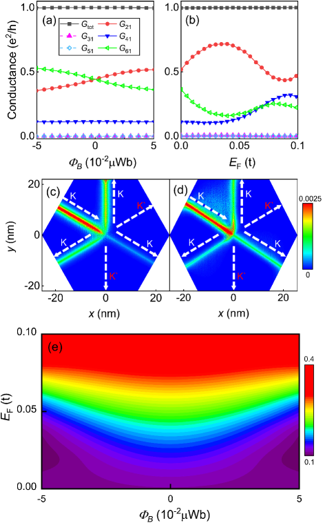
Influence of Magnetic Field—. In addition to control through electrical means, current partition is also strongly affected by applying a magnetic field. The effect of a magnetic field can be included by attaching a Peierls phase factor to the following hopping term:
where is the integral of the vector potential along the path from site to . The presence of a magnetic field changes the current partition as shown in Fig. 2(a) for and . We find that the presence of the magnetic field removes the equality between and because the magnetic field breaks the mirror reflection symmetry. However, the forward-propagating current remains unaffected.
By changing under a given magnetic field as shown in Fig. 2(b), we find that the current partition to both forward and side directions vary simultaneously. As approaches the bulk band edge, the current partitioned to T4 increases gradually but does not reach the same magnitude as that for vanishing magnetic flux. Figures 2(c) and (d) show more clearly the current partition under a magnetic flux of for and , respectively, wherein more current is partitioned into T2 than into T6. This difference is more obvious at the higher Fermi energy, in agreement with previous work networkwk ; magneticfieldwk .
To show the influences of magnetic field and Fermi energy more systematically, in Fig. 2(e) we show the phase diagram for conductance with different values of and . is only weakly dependent on the magnetic field as approaches CNP and the bulk band edges but is strongly dependent on the magnetic field in the middle region.
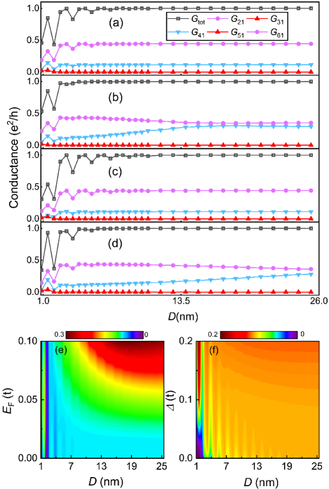
Effect of System Size—. For an electronic nanodevice, its size plays a crucial role. Herein, we investigate the current partition of a device whose circumcircle diameter ranges from 1 nm to 25 nm. In Figs. 3(a)–(d), we plot the current partition as a function of at different Fermi energies and staggered sublattice potential . The current partition fluctuates obviously for nm, which is mainly due to the backscattering because the total conductance is not quantized. When the system size increases, the backscattering vanishes. However, increasing the system size has only a weak influence on the current partition when is close to CNP but has a definite influence to bring and closer together when lies at the band edge. Such a behavior suggests that the equal-current partition approximation is valid at small twist angle but invalid at large twist angle when the Fermi energy is far away from charge neutrality.
The length dependence of the current partition at different with is shown in Fig. 3(e), wherein the fluctuation appears for small sizes and exhibits weak dependence on . As the system size increases, gradually increases and then saturates at a magnitude that increases with . By setting , we plot the phase diagram of as function of the energy gap and circumcircle diameter in Fig. 3(f), wherein similar behaviors are observed. Moreover, we find that the saturated at larger size also increases with the energy gap.
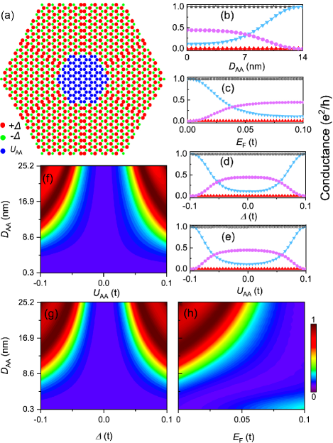
Effect of AA Stacking Size—. We now study how the AA stacking size at the intersection affects the current partition, as shown schematically in Fig. 4(a). This can simulate the effect of the twisting angle in t-BG, where the size of AA stacking zone shrinks for smaller twist angle Morie . We vary the circumcircle diameter of the AA stacking region, namely , from the smallest size to 25.2 nm while fixing the device size as nm. With and , we find that increases with and becomes quantized at nm, where the current partition of vanishes. This behavior suggests that the central AA stacking region acts as a scattering zone whose scattering weakens as its size increases, thereby increasing the forward-propagation current. As a result, most of the current flows along one zero-line, with weak partition to the other allowed zero-lines.
For the largest AA stacking region, i.e., when there is no longer an energy gap in the central scattering region, the current is fully partitioned into the forward-propagating zero-line. By changing from CNP, we find that the current partition becomes tunable. As we increase , first decreases and then increases to the quantized value near . When we further increase , decreases to a small value. For nm and , the current partitioned into grows with and those into and decrease.
Note that all of the above results were calculated under the condition that . For and , we find that increases with and becomes quantized at , where the current partitioning of vanishes.
In Fig. 4(f), we plot the phase diagram of with different and at fixed and ; for , no longer influences the current partitioning. In Fig. 4(g), we also plot the phase diagram of with different and at fixed . Now, the resonant transmission appears for a different band gap . As we decrease from , the value of for resonant transmission increases until it equals 25.2 nm, and the resonant transmission disappears when . Figure 4(h) plots the phase diagram of with different and at fixed . One finds that the resonant transmission appears at and the resonant diameter increases with . Note that at the resonant transmission point of and nm, increasing drives to decrease gradually as in Fig. 4(c), suggesting that the current partition goes from zero to a finite value. Such tunability by means of electric gating could be used to construct a field-effect transistor based on the dissipationless topological ZLMs for switching on and off the forward propagation.
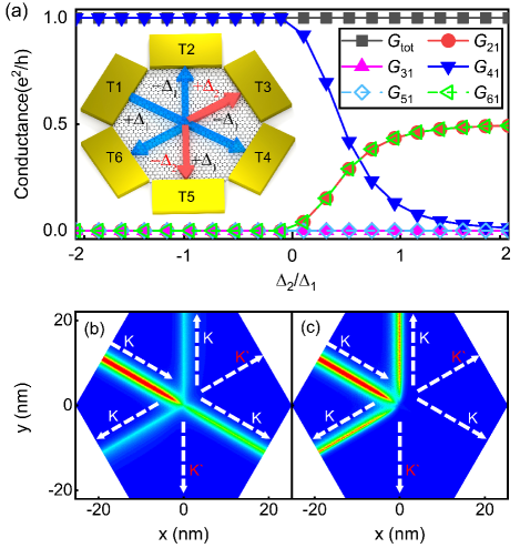
Tunable valley-current splitter— In order to control the current partition effectively and quantitatively, we add two set of electric field and on the six terminal device, as shown in the insert of Fig. 5(a). We vary the magnitude of while fixing the , device size as and . We find that becomes quantized when , where the current partition of vanishes, which means there only exit a single zero-line. With , we find that decreases and increase with . When , become the same value, where present the intersection of three zero-lines. When we further increase to 2, decrease to zero and become 0.5 , as shown in Fig. 5(c), where shows the current partition just like the intersection of two zero-lines. By fixing one of the electric field and vary the other, we can modulate the partition from zero to quantized, precisely, making this device more qualified as a valley-current splitter.
Summary—. We presented a systematic study of the electronic transport properties of three intersecting zero-lines in a twisted bilayer graphene, which form six topological zones stacked either in AB or BA patters and is centered in a gapless region with AA stacking. We investigated the influence of system size, AA-region size, , energy gap, and magnetic field on the current partitioning. When current flows through the device, the forward-propagating current partitioning is nonzero and can be tuned by mediating . This is in contrast to the topological intersection of two zero-lines, where forward propagation is forbidden.
When the central AA region is small, increasing to the band edge enhances to partition the current into three nearly equal zero-lines, and the potential of the AA region does not affect the current partitioning. By making the central AA region larger, which corresponds to decreasing the twist angle, resonant forward transmission can be realized at a proper , in which case the partitioning to the side zero-lines vanishes. Starting from the case of resonant transmission, further increasing (e.g., by means of electric gating) increases the current partitioning to the side zero-lines from zero to a definite level, thereby suggesting that the system could be used as a dissipationless field-effect transistor. Moreover, decreasing the system size gives rise to strong backscattering and conductance fluctuations. In the absence of a magnetic field, the symmetric geometry of our central region leads to current partitioning, but the presence of a magnetic field breaks this symmetry.
Our theoretically proposed device can pericely find its experimental realization in graphene moiré structures, and can also find realizations in phononic crystals. Specifically, our findings are the first prediction of the current partition at the zero-line intersection node of a triangular network of topological channels in small twist angle bilayer graphene and paves the way towards the realization of low-power topological quantum devices.
Acknowledgements.
Acknowledgments—. This work was supported financially by the National Key R & D Program (2017YFB0405703 and 2016YFA0301700), and the NNSFC (11474265, and 11674024), the China Government Youth 1000-Plan Talent Program, and Anhui Initiative in Quantum Information Technologies. We are grateful to AMHPC and Supercomputing Center of USTC for providing high-performance computing assistance.References
- (1) Huang, S.; Kim, K.; Efimkin, D.-K.; Lovorn, T.; Taniguchi, T.; Watanabe, K.; MacDonald, A.-H.; Tutuc, E.; LeRoy, B.-J. Topologically Protected Helical States in Minimally Twisted Bilayer Graphene. Phys. Rev. Lett. 121, 37702 (2018).
- (2) Rickhaus, P.; Wallbank, J.; Slizovskiy, S.; Pisoni, R.; Overweg, H.; Lee, Y.; Eich, M.; Liu, M.; Watanabe, K.; Taniguchi, T.; Fal’ko, V.; Ihn, T.; Ensslin, K. Transport Through a Network of Topological Channels in Twisted Bilayer Graphene. Nano Lett., 11, 6725 (2018)
- (3) Ramires, A.; Lado, J.-L. Electrically Tunable Gauge Fields in Tiny-Angle Twisted Bilayer Graphene. Phys. Rev. Lett. 121, 146801 (2018)
- (4) Efimkin, D.-K.; MacDonald, A.-H. Helical network model for twisted bilayer graphene. Phys. Rev. B. 98, 035404 (2018)
- (5) Makwana, M.-P.; Craster, R.-V. Designing multidirectional energy splitters and topological valley supernetworks. Phys. Rev. B. 98, 235125 (2018)
- (6) Jose, P.-S.; Prada, E. Helical networks in twisted bilayer graphene under interlayer bias. Phys. Rev. B. 88, 121408(R) (2013)
- (7) Qiao, J.-B.; Yin, L. J.; He, L. Phys. Rev. B. Twisted graphene bilayer around the first magic angle engineered by heterostrain. 98, 235402 (2018)
- (8) Sunku, S.-S.; Ni, G.-X.; Jiang, B.-Y.; Yoo, H.; Sternbach, A.; McLeod, A.-S.; Stauber, T.; Xiong, L.; Taniguchi, T.; Watanabe, K.; Kim, P.; Fogler, M.-M.; Basov, D.-N. Photonic crystals for nano-light in moiré graphene superlattices. Science 362, 1153-1156 (2018)
- (9) Wang, K.; Ren, Y.-F.; Deng, X.-Z.; Yang, S.-A.; Jung, J.; Qiao, Z. H. Gate-tunable current partition in graphene-based topological zero lines. Phys. Rev. B. 95, 245420 (2017).
- (10) Wang, K.; Hou, T.; Ren, Y.-F.; Qiao, Z.-H. Enhanced robustness of zero-line modes in graphene via magnetic field. Front. Phys. 14, 23501 (2019).
- (11) Li, J.; Zhang, R.; Yin, Z.; Zhang, J.; Watanabe, K.; Taniguchi, T.; Liu, C.; Zhu, J. A valley valve and electron beam splitter. Science 362, 11491152 (2018)
- (12) Aldena, J.-S.; Tsena, A.-W.; Huanga, P.-Y.; Hovdena, R.; Brownb, L.; Park, J.; Muller, D.-A.; McEuen, P.-L. Strain solitons and topological defects in bilayer graphene. PNAS 110 11256-11260 (2013)
- (13) Yankowitz, M.; Jung, J.; Laksono, E.; Leconte, N.; Chittari, B. L.; Watanabe, K.; taniguchi, T.; Adam, S.; Graf, D.; Dean, C. Dynamic band-structure tuning of graphene moiré superlattices with pressure. Nature 557, 404 (2018)
- (14) Kim, H.; Leconte, N.; Chittari, B. L.; Watanabe, K.; Taniguchi, T.; MacDonald, A.-H.; Jung, J.; Jung, S. Accurate Gap Determination in Monolayer and Bilayer Graphene/h-BN Moiré Superlattices. Nano Lett. 18, 7732 (2018)
- (15) Hou, T.; Chen, G.-H.; Tse, W-K.; Zeng, C.-G.; Qiao, Z.-H. Topological zero-line modes in folded bilayer graphene. Phys. Rev. B 98, 245417 (2018)
- (16) Martin, I.; Blanter, M.; Morpurgo, A.-F. Topological Confinement in Bilayer Graphene. Phys. Rev. Lett. 100, 036804 (2008).
- (17) Qiao, Z. H.; Jung, J.; Niu, Q.; MacDonald, A.-H. Electronic Highways in Bilayer Graphene. Nano Lett. 11, 3453 (2011).
- (18) Qiao, Z. H.; Jung, J.; Lin, C.; Ren, Y.-F.; MacDonald, A. H.; Niu, Q. Current Partition at Topological Channel Intersections. Phys. Rev. Lett. 112, 206601 (2014).
- (19) Jung, J.; Zhang, F.; Qiao, Z. H.; MacDonald, A. H. Valley-Hall kink and edge states in multilayer graphene. Phys. Rev. B 84, 075418 (2011)
- (20) Zhang, Y.-T.; Qiao, Z.-H.; Sun, Q.-F. Detecting zero-line mode in bilayer graphene via the quantum Hall effect. Phys. Rev. B 87, 235405 (2013)
- (21) Bi, X.-T.; Jung, J.; Qiao, Z.-H. Role of geometry and topological defects in the one-dimensional zero-line modes of graphene. Phys. Rev. B 92, 235421 (2015)
- (22) Lee, C.; Kim, G.; Jung, J.; Min, H. Zero-line modes at stacking faulted domain walls in multilayer graphene. Phys. Rev. B 94, 125438 (2016)
- (23) Kim, M.; Choi, J. H.; Lee, S. H.; Watanabe, K.; Taniguchi, T.; Jhi, S.-H.; Lee, H.-J. Valley-symmetry-preserved transport in ballistic graphene with gate-defined carrier guiding. Nat. Phys. 12, 1022 (2016).
- (24) Ju, L.; Shi, Z.; Nair, N.; Lv, Y.; Jin, C.; Jr, J-V; Bechtel, H. A.; Martin, M.-C.; Zettl, A.; Analytis, J.; Wang, F. Topological valley transport at bilayer graphene domain walls. Nature (London) 520, 650 (2015).
- (25) Kim, M.; Choi, J. H.; Lee, S. H.; Watanabe, K.; Taniguchi, T.; Jhi, S.-H.; Lee, H.-J. Valley-symmetry-preserved transport in ballistic graphene with gate-defined carrier guiding. Nat. Phys. 12, 1022 (2016).
- (26) Yan, M.; Lu, J.; Li, F.; Deng, W.; Huang, X.; Ma, J.; Liu, Z. On-chip valley topological materials for elastic wave manipulation. Nat. Material. 17, 993 (2018)
- (27) Li, J.; Wang, K.; Kenton, J.-M.; Zern, Z.; Ren, Y.-F.; Watanabe, K.; Taniguchi, T.; Qiao, Z.-H.; Zhu, J. Gate-controlled topological conducting channels in bilayer graphene. Nat. Nanotechnol. 11, 1060 (2016).
- (28) Datta, S. Electronic Transport in Mesoscopic Systems. (Cambridge University Press, 1997).
- (29) Wang, J.; Guo, H. Relation between nonequilibrium Green’s function and Lippmann-Schwinger formalism in the first-principles quantum transport theory. Phys. Rev. B 79, 045119 (2009).
- (30) Yin, L.; Qiao, J.; Zuo, W.; Li, W.; He, L. Experimental evidence for non-Abelian gauge potentials in twisted graphene bilayers. Phys. Rev. B 92, 081406 (2015)