Valley caloritronics in a photodriven heterojunction of Dirac materials
Abstract
We consider a lateral hetero-junction where the left and right leads are made of monolayer graphene and the middle region is made of a gapped tilted Dirac material (borophene or quinoid graphene) illuminated with off-resonant circularly polarized radiation. The tilt parameter makes the band gap indirect and smaller in magnitude as compared to Dirac materials without tilt. Exposure to radiation makes the band gaps of the central region valley-dependent which show their signatures as valley polarized charge and thermal currents, thereby causing a valley Seebeck effect. We study the variation of the valley polarized electrical conductance, thermal conductance, thermopower and figure of merit of this junction with chemical potential and a tunable gap parameter . For non-zero , all the valley polarized quantities are peaked at certain values of chemical potential and then vanish asymptotically. Increase in gap parameter enhances the valley thermopower and valley figure of merit, whereas the valley conductances (electrical and thermal) show non monotonic behavior with . We also compare the valley polarized quantities with their corresponding charge counterparts (effective contribution from both the valleys). The charge thermopower and the charge figure of merit behave non monotonically with and the charge conductances (electrical and thermal) depict a decreasing trend with . Furthermore, the tilt parameter reduces the effective transmission of carriers through the junction, thereby diminishing all the charge and valley polarized quantities. As the gaps in the dispersion can be adjusted by varying the intensity of light as well as the Semenoff mass, the tunability of this junction with regard to its thermoelectric properties may be experimentally realizable.
I Introduction
Thermoelectric materials have attracted immense interest in energy efficient device applications [1, 2, 3, 4, 5, 6, 7, 8, 9, 10, 11, 12, 13]. The efficiency of power generation in such devices depends on the interplay between their electronic and thermal performances and it is characterized by a dimensionless quantity called figure of merit, , where , and denote electrical conductivity, thermal conductivity and Seebeck coefficient (thermopower), respectively, with being the absolute temperature. In bulk materials, the factors in the expression of are mutually coupled in such a way that it is difficult to control them independently, and hence improve . The techniques used to improve the figure of merit rely on enhancing the power factor () and lowering the thermal conductivity. One of the important proposals is nanostructuring of materials which enhances thermoelectric efficiency due to the sharply peaked density of states (DOS) of the carriers in low-dimensional materials [1, 14]. Another useful method is engineering the band structure [15, 16] in conjunction with nanostructuring to lower the thermal conductivity. Further, the use of semi-metals with large electron-hole asymmetry can enhance the thermoelectric coefficients [17].
Advancements in fabrication technologies have opened up new ways of exploring two-dimensional materials for thermoelectric applications[7, 8, 9, 10, 11]. Since the realization of graphene [18, 19] there have been numerous experimental and theoretical studies of quasi-2D materials supporting Dirac cones such as silicene [20], germanene [21], and MoS2 [22]. Recently, there has been immense interest in synthesis of 2D crystalline boron structures, generally known as borophene [23, 24, 25]. One of them is 8- borophene, which is is a zero gap semiconductor with tilted anisotropic Dirac cones [26, 27, 28] and can be thought of as topologically equivalent to quinoid graphene [29, 30]. The bulk optical [31], magnetotransport [32], collective modes [33], Floquet states [34] and thermoelectric properties [35] of this borophene structure have been studied extensively. Another experimentally synthesized allotrope of boron is borophene whose band structure and electronic properties have been extensively studied [36, 37]. Besides, a very recent success of integrating dissimilar two-dimensional (2D) materials [38] which is essential for nano-electronic applications, has opened a new direction for studying the thermoelectricity in junction devices of different materials. In Ref. [38], the authors have reported the covalent lateral stitching of borophene-graphene, resulting in rare realization of 2D lateral hetero-structure where the lateral interfaces are atomically sharp despite imperfect crystallographic lattice and symmetry matching. Furthermore, a graphene/quinoid graphene/graphene junction can be realized by taking a single graphene sheet, where the middle region is deformed (quinoid graphene) by applying a uniaxial strain.
The concept of valleytronics [39, 40, 41, 42], similar to spintronics [43, 44, 45, 46, 47, 48], is becoming popular in recent past. In valleytronic devices, the information is carried by the valley degree of freedom of the charge carriers. The generation of valley polarization and optically excited valley-polarized current in various materials have been studied theoretically as well as experimentally [49, 50, 51, 52]. The harnessing of internal degrees of freedom like spin/valley of the charge carriers by applying thermal gradient and the associated phenomena are called spin/valley caloritronics.
Motivated by the above discussion, we study the thermoelectric effects of a nano-junction system where the left and right electrodes are made of graphene and the middle region is made of 2D Dirac material having tilted anisotropic Dirac cones, such as borophene or quinoid graphene. The middle region has different onsite energies on the two sublattices and is subjected to circularly polarized electromagnetic radiation. It results in valley dependent bands at the two Dirac points and hence a valley dependent transmission probability. Thus, in analogy with the spin-caloritronic studies, thermally activated quantum transport of valley degree of freedom of the charge carriers can be achieved. Our goal is to study thermally driven valley polarized properties, known as valley caloritronics and compare them with that of the charge caloritronics in detail.
This paper is organized as follows. In Sec. (II), we present basic information of the lateral junction (Subsec. (II.1)) and the definitions of different thermoelectric coefficients (Subsec. (II.2)). All the numerical results and their corresponding discussions are presented in Sec. (III). Finally, we conclude and summarize our main results in Sec. (IV).
II Model and Theoretical Methods
Here, we first present the essential information of the junction characterized by the quasi-ballistic transport. Later we present general description of Seebeck coefficient, electrical conductance, thermal conductance and figure of merit for any junction device. The discussions in Sec. (II.2) are applicable to any junction characterized by the quasi-ballistic transport.
II.1 Basic information of the junction
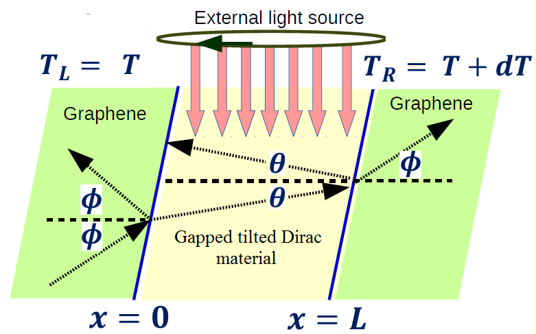
We consider a two-dimensional junction system placed on the plane at room temperature as shown in Fig. (1). The left () and right () leads are made of graphene sheets, while the middle region () is made of a 2D material hosting tilted anisotropic Dirac dispersion (can be considered as borophene or quinoid graphene) with a mass gap at low energy. Further, it is assumed that the middle region is subjected to a circularly polarized electromagnetic radiation where the photon energy satisfies the off-resonant condition, i.e., the photon energy is much higher than the band width of the undriven lattice in the middle region of the system. The off-resonant circularly polarized light induces a gap in the energy dispersion.
The Hamiltonian for the charge carriers in graphene sheet in the vicinity of the Dirac points is given by [29]
| (1) |
where denotes two independent Dirac points, m/s is the Fermi velocity, , are the Pauli matrices denoting the sublattice degrees of freedom. The corresponding energy dispersion of the Hamiltonian in Eq. (1) is given by , independent of the valley pseudo-spin , where denotes the conduction and valance bands, respectively. The corresponding eigenfunctions are given by
| (2) |
where .
The effective Floquet Hamiltonian, describing the charge carriers of the middle region (tilted anisotropic borophene or quinoid graphene) subjected to circularly polarized electromagnetic radiation, in the vicinity of the two independent Dirac points can be written as [53] (see Appendix A),
| (3) |
Here, is the identity matrix and is the net valley-dependent mass resulting from the valley-dependent photoinduced mass [54] and different onsite energies on the two sublattices [55], with being the Semenoff mass. The photoinduced mass is proportional to the intensity of light, which can be tuned experimentally. A tunable Semenoff mass has been experimentally achieved in graphene by placing it appropriately on hexagonal boron nitride substrate [56] or by applying an electric field normal to its plane [57] (which breaks inversion symmetry). Using similar techniques, the creation of such a mass gap may be possible in borophene as well, although its experimental realization is still not known. We define a dimensionless parameter such that . Here, are the direction dependent velocities where (tilt parameter) is responsible for the tilt in energy dispersion. The values of these velocities for borophene are , and [27]. The energy dispersion and the corresponding wave functions associated with the Hamiltonian in Eq. (3) are given by
| (4) |
and
| (5) |
where with , and having dimension of velocity.
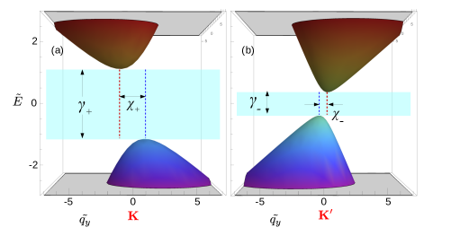
The band structure of borophene in the two valleys with valley-dependent masses is shown in Fig. (2) for . The system is an insulator with valley-dependent indirect band gaps . The shift between maxima of valence band and minima of conduction band in both the valleys is along the axis. The magnitude of the indirect gaps and the shifts are given as
| (6) |
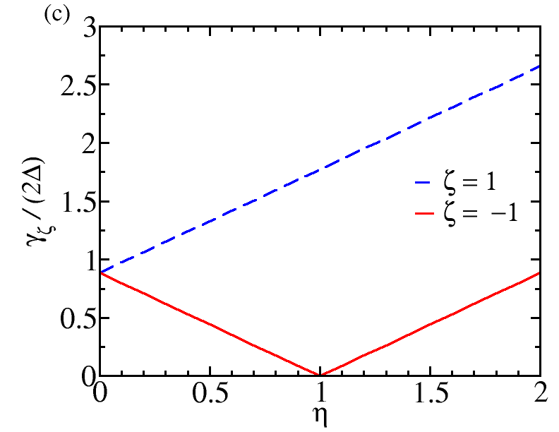
Equation (6) reveals that the band gaps reduce due to tilt and decrease monotonically with for while the shifts corresponding to the gaps increase. For , the band gap at valley is smaller than at valley. So, the effective band gap of the system is . The direct gaps at the original Dirac points are equal to . The magnitude of the gap at valley monotonically increases with , whereas for valley, it initially decreases with (for ), vanishes at and then starts to increase again for (see Fig. (2c)).
The middle region can be reduced to a gapped graphene by setting and , so that the junction becomes a graphene/gapped-graphene/graphene junction. If the Fermi energy lies in the gap, the middle region behaves like a topological insulator when , otherwise it is a trivial insulator. In the topological insulating state, the edge states contribute to the transport quantities. Since our system is kept at room temperature, the contribution from the bulk states would dominate over the edge states contribution [58].
Suppose an electron from the left lead is injected with an energy and incident angle . The valley-dependent transmission probability of the electron from left to right lead is obtained as (see appendix B)
| (7) |
where is given by
| (8) |
The values of and in the expression of can be obtained by solving the following two coupled equations:
| (9) | |||||
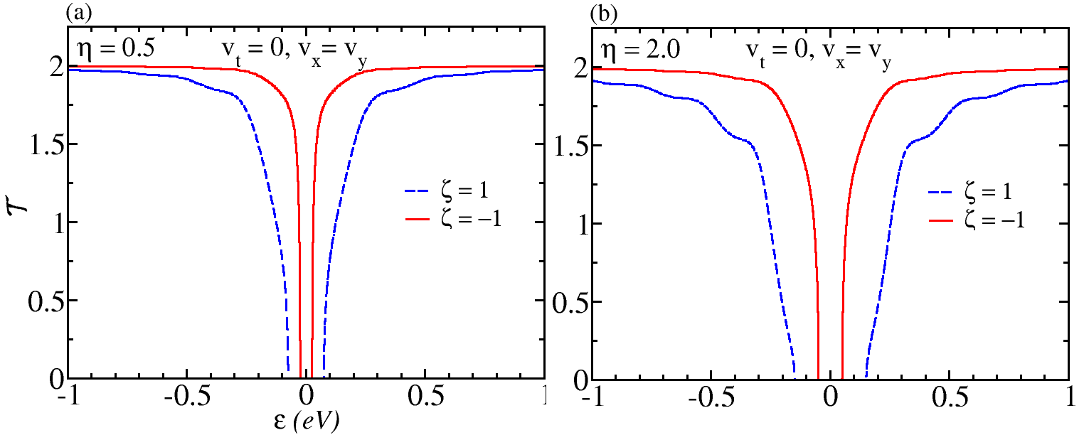
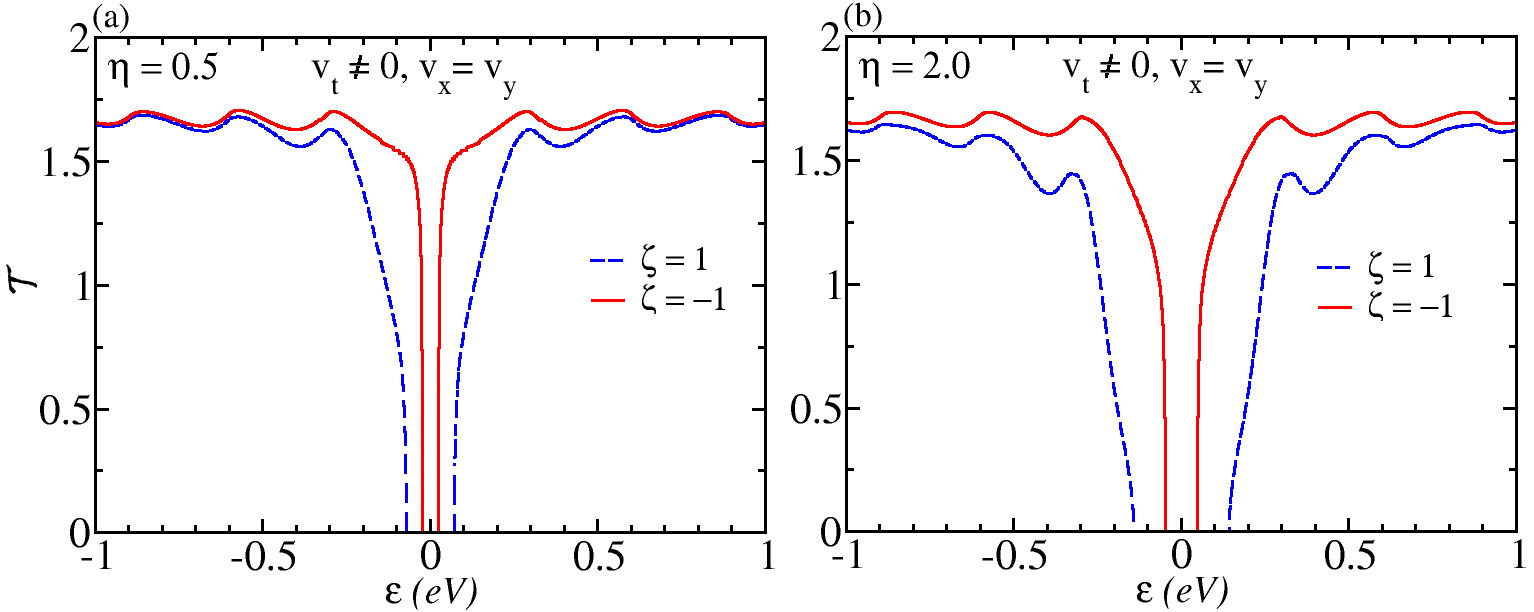
We define the effective transmission coefficient for current along direction at a given energy as . In Figs. (3), (4), vs. is plotted for two conditions – , and , . The oscillations in in Fig. (4) appear due to the term (see Eq. (37)), where is a function of . In case of , and , the values of the and become equal and becomes , which eventually yields the coefficient of to be and thus becomes (see Eq. (37)) and . As a result no such noticeable oscillations are obtained (see red curves of Figs. (3a) and (3b)). The physics behind this can be explained using the concept of electron wave interference – when , and , the system can be viewed as a single graphene sheet without any barrier. Thus, almost all the incoming electron waves from the left lead get transmitted to the right lead, leaving almost no reflected wave and thereby causing no interference. If the band gap is further increased, the probability of the reflection of electron waves from the interface increases; so the reflected and the transmitted electron waves begin to interfere. This results in oscillations in the transmission probability for , case as well (see blue curves in Figs. (3a) and (3b)). Furthermore, the valley has smaller as compared to valley. It can be understood using the analogy of transmission through a rectangular potential barrier. If the middle region is considered as a potential barrier with a barrier height , the transmission probability is smaller for a larger barrier height for the considered range of incident energies above the barrier. Since , valley allows lesser transmission than .
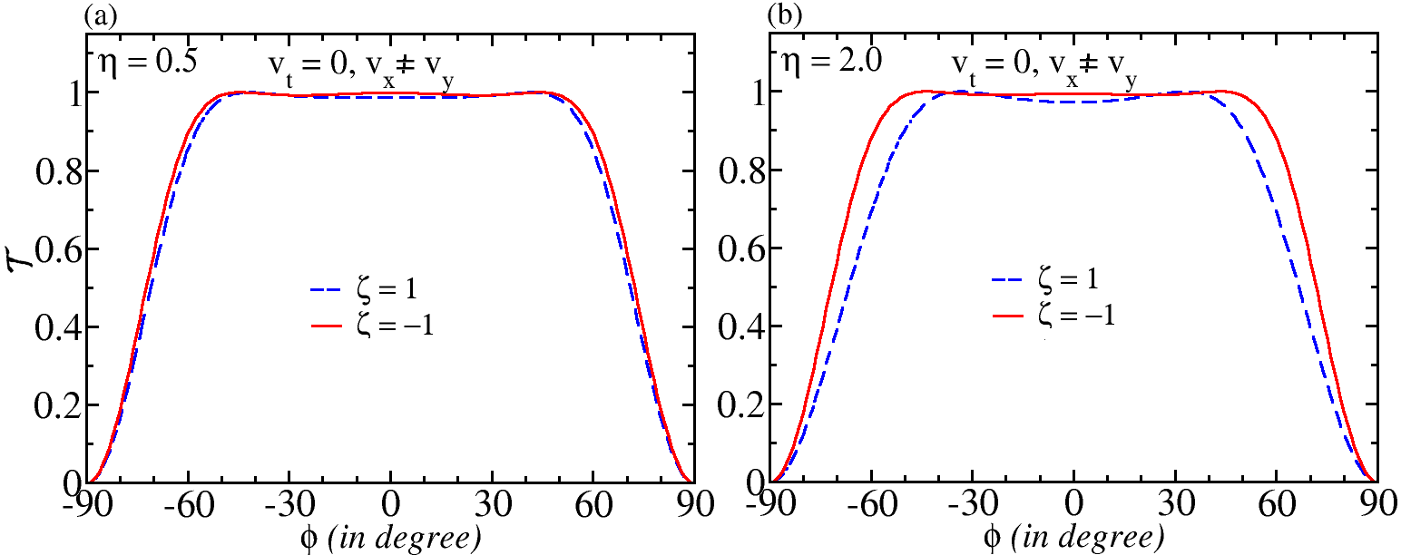
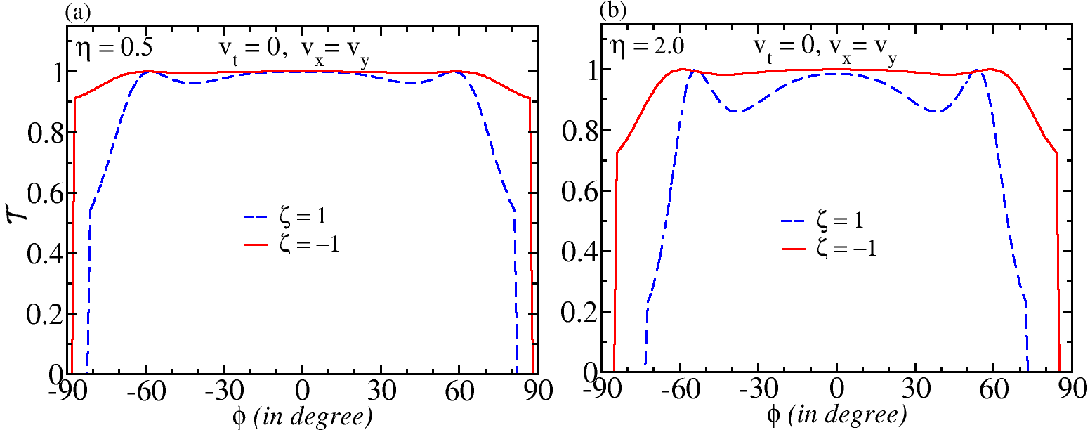
The tilted velocity term diminishes , as for the transmission probability as a function of incident angle shows more deviation from compared to case (see Figs. (9), (10) and (11)). Moreover, the is almost electron-hole symmetric (see Figs. (3), (4)) although breaks the electron hole symmetry in band structure (see Fig. (2)).
II.2 Thermoelectric coefficients
A detailed derivation of the thermoelectric coefficients is given in appendix (C). The valley resolved Seebeck coefficient for a small temperature difference is given as
| (10) |
where are the valley-resolved thermoemfs induced between the cold and hot leads and are the kinetic coefficients for quasi-ballistic transport given by
with .
At zero external bias voltage , the valley resolved electrical conductance can be expressed as
| (12) |
where is the valley-dependent charge current given in Eq. (38).
The valley resolved thermal conductance associated with the valley-dependent thermal currents can be expressed in terms of the kinetic coefficients (see Eq. (II.2)) as [59, 60]
| (13) |
The total charge and thermal conductance are defined as and . Similar to Ref. [46, 47], we define the charge Seebeck coefficient as . The charge Seebeck coefficient can be viewed as the effective thermoemf generated between the two leads per unit temperature difference.
In this system, the carriers in the two valleys have unequal transmission probabilities owing to distinctive nature of the valley gaps. So, the heat and particle flux in the two valleys differ, giving rise to valley polarized charge currents and thermal currents . This leads to different induced voltages in the two valleys at the cold lead. Thus, the two valleys act as two conducting channels having different thermopowers present within the same system. Since the transfer of electrons between the valleys is prohibited due to large separation of the valleys in (quasi)momentum space and absence of any valley-mixing mechanism, a valley emf () exists. This phenomenon can be termed as the valley Seebeck effect analogous to the spin Seebeck effect [43]. It refers to the generation of a valley voltage resulting from a temperature gradient.
Using the same analogy as in Ref. [48] for spin Seebeck coefficient, the valley Seebeck coefficient is defined as . Similar to the spin Seebeck effect [43], the valley Seebeck coefficient can be viewed as the potential difference between charge carriers of the two valleys in the cold lead per unit temperature difference. Similar to the valley current, the valley polarized electrical conductance and the valley polarized thermal conductance can be defined as and respectively.
One of the challenges in fabricating thermoelectric devices is to obtain optimal conditions which ensure the operation of the device with maximum power output at the best possible efficiency. The efficiency of the system depends upon a quantity called the figure of merit which is defined as
| (14) |
where is charge Seebeck coefficient, is the charge conductance, is the thermal conductance of the carriers, is phonon’s thermal conductance owing to the involvement of lattice structure and is the absolute temperature. The possibility of extracting the valley thermoemf for power generation allows us to define valley figure of merit of this device using the same analogy as spin figure of merit in Ref. [61, 48, 62, 63].
In the context of phononic contribution to thermal conductance, we would like to mention that the Debye temperature in borophene has a high value about K [64, 65] due to the strong bonding. Further, graphene has also a higher Debye temperature K, approximately an order of magnitude higher than for typical metals. Thus, the room temperature ( K) is safely assumed to be low with respect to high Debye temperatures of borophene and graphene. Due to this reason, the phonon population is expected to be low at room temperature, which diminishes the possibility of phonon-phonon inelastic scattering events. Henceforth we neglect the phonon’s contribution in thermal conductance.
III Results and Discussion
Here we present numerical results of different thermoelectric properties of the junction subjected to the off-resonant Floquet radiation. For our numerical analysis, we choose the parameters and eV. The dimensionless parameter, is varied in the range []. It should be noted that with increasing value further, the conductance in valley vanishes in the low chemical potential region. As our main goal is to study the valley polarized properties, to get non-zero values of the conductance for both the valleys, we choose the maximum . Temperature of the cold lead is maintained at K and that of the hot lead is where . The dimensions of system are taken as nm.
III.1 VALLEY ELECTRICAL CONDUCTANCE
The variation of and with chemical potential for different values of are shown in Fig. (5a) and Fig. (5b) respectively.
(a) Dependence on chemical potential:
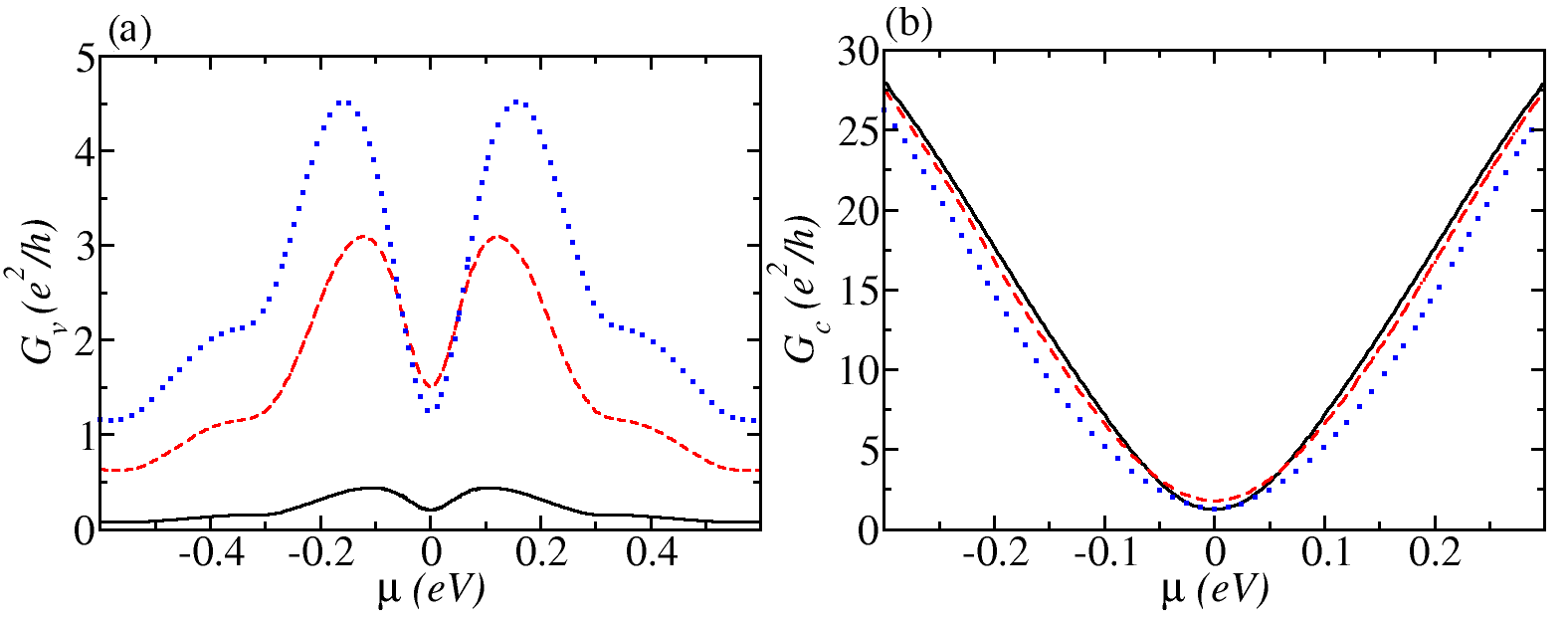
The valley polarized conductance has peaks at and a local minimum at (Fig. 5a). This feature is also present when the middle region is gapped graphene with unequal masses in the two valleys, which indicates that tilt is not responsible for the peaks. The appearance of peaks can be explained using an analogy with transmission through a rectangular barrier. For gapped graphene, the dispersion can be approximated as near the band minima/maxima. So, the middle region can be viewed as a potential barrier with valley-dependent barrier heights () and effective masses . The rate of increase of transmission with for smaller mass () is higher than that with larger mass () for energies just above the barrier (see Figs. (3) and (4)). Since is proportional to , increases slowly with resembling a quadratic growth, while rises sharply resembling almost a linear growth due to smaller mass. For higher value of , the effect of mass in the dispersion becomes negligible in both the valleys which results in almost similar variation of their conductances with . Due to this nature, increases with initially, attains a maximum (peak) and then decreases asymptotically to zero at higher .
On the other hand, increases monotonically with increase in (Fig. 5b). This is primarily due to the increase in the number of available conducting channels in the leads with increase in . As expected, is always greater than for a given .
(b) Dependence on gap parameter: The valley conductance increases with the increasing strength of for and starts to decrease with for . This can be explained as follows – Since a larger gap corresponds to lesser , the increase in lowers , owing to the monotonic rise in with (see Fig. 2(c)). Similarly, due to the non-monotonic variation of , initially increases with , attains maximum value at and then starts to decrease with . Since increases while decreases with for , their difference gets enhanced with . For , both and decrease with , but the rate of decrease of is more than that of . As a result, gets diminished with for . For , we get which yields . On integrating out , both the valleys give the same value of transmission at a given energy. Hence, as .
Figure 5(b) reveals that gets diminished (though the change is small, but noticeable)
with increasing , away from the low chemical potential regime. Near the low chemical
potential region, there are crossovers in the conductance plots.
The tilt diminishes in each valley, which results in lowering of . It is found that also decreases with , since diminishes as well (see Figs. (3) and (4)). It is interesting to note that charge and valley conductances show high degree of electron-hole symmetry despite the fact that the spectrum in the middle region is electron-hole asymmetric due to non-zero . Similar behaviour is shown in bulk borophene [35].
III.2 VALLEY SEEBECK COEFFICIENT (THERMOPOWER)
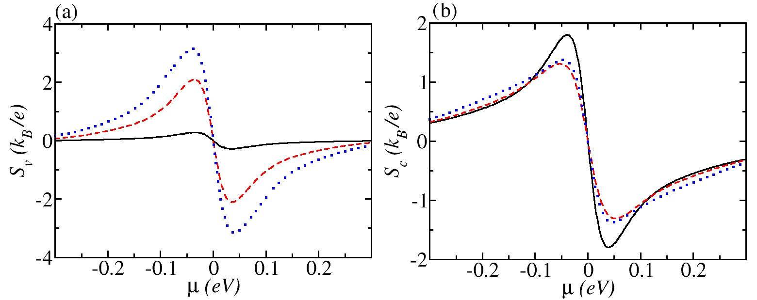
The valley and charge Seebeck coefficients and (in units of ) as a function of the chemical potential for various values of are shown in Fig. (6a) and Fig. (6b) respectively .
(a) Dependence on chemical potential: Both and display a local maxima (minima) at eV on variation with . The value of is roughly independent of . The maxima/ minima in the thermopower arises due to the term in the numerator of Seebeck coefficient (see Eq. (40)). There is a change in sign of while change in sign of (due to term in the numerator of ). It indicates the change in electrical nature of the charge carriers as changes sign. When lies in the conduction (valence) band, thermally activated electrons (holes) propagate opposite (parallel) to the temperature gradient, which results in negative (positive) thermopower. Similar to the conductance, the electron-hole symmetry is nearly perfect in the absolute value of Seebeck coefficients.
(b) Dependence on gap parameter: The absolute values of increase with at a given chemical potential. This can be explained as follows – From the definition of Seebeck coefficient , we can say that increase in and decrease in with aid to enhance the value of . Since increases and decreases with , starts to gain weight as we increase . Similarly, initially decreases with , attains minimum at and again starts to increase. Though and show different nature of variation with , their difference as a function of is mainly dictated by . This happens because valley’s contribution in thermopower changes more rapidly with as compared to valley . The behavior of valley thermopower as a function of can be understood from Fig. (6(c)) also. As the ratio of and increases with , the valley thermopower gets enhanced with increasing strength of . The reason behind this can be understood from Fig. (4), as it reveals that with increasing from to , the rate of change in in valley is more than that in valley.
For the chemical potential eV, the charge thermopower decreases with for , attains minima around , and then starts increasing again. For eV, an increase in aids to enhance , though the enhancement is quite small. So and behave differently with which is mainly due to the different weightages of and channels’ contribution in their definitions. It seems that on increasing the strength of even more, one can achieve higher valley thermopower. But it is not possible, as for such a higher value of , there will be no available channel to conduct in the low chemical potential regime.
It is worth mentioning that decrease with . Though diminishes (denominator of ), it lowers (numerator of ) too. Hence, the contribution of (see definition of ) decreases as we increase . The charge thermopower also behaves similarly as a function of .
The materials with large electron-hole asymmetry are known to enhance the thermoelectric coefficient. So more thermopower is expected when the middle region is made of tilted Dirac material instead of graphene. But does not break the electron-hole symmetric nature in as shown in Fig. (4)). Hence, it cannot aid to enhance the thermopower of the system. It is to be noted that if the middle region is also monolayer graphene, then for higher value of , we do not get any thermopower in the low chemical potential regime, whereas if the middle region is borophene or quinoid graphene, we get finite values of thermopower for those low values of chemical potential. The physics behind this as follows – for graphene, in case of , there is no transmission because of imaginary momentum, and thus no channel to conduct. But for borophene or quinoid graphene, due to the indirect gap for the tilted velocity term, the momentum is real until , and hence few channels are available to conduct, although (See Eq. (6) and Fig. (2)). Thus for low chemical potential, the highly gapped graphene-borophene-graphene junction is good candidate with respect to highly gapped graphene-graphene-graphene junction as a thermoelectric device.
III.3 VALLEY THERMAL CONDUCTANCE
The valley polarized thermal conductance and charge thermal conductance as a function of are shown in Fig. (7a) and Fig. (7b) respectively for different values of .
(a) Dependence on chemical potential:
As the valley resolved thermal conductance arises due to the energy flow carried by the charge carriers, as a function of shows almost similar features as except the region where is close to zero. In the case of (see Figs. (7a) and (7b) ) there is a bump near , while for there is no such thing. This bump in arises due to the term as shown in the inset of Fig. (7b), whereas valley (in addition to valley ) is also responsible for the bump in (see inset of Fig. (7a)). Moreover, the valley thermal conductance has peaks at and then starts decreasing with (similar to ), as opposed to .
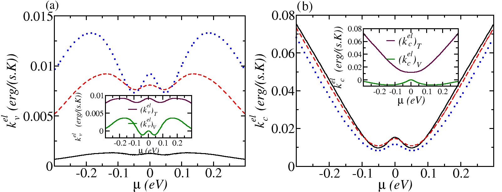
(b) Dependence on gap parameter: As expected, shows the same nature as the electrical charge conductance as a function of , which is depicted in Fig. (7). The reason behind this nature is same as for the charge conductance.
Not surprisingly, as a function of shows the similar behavior as electrical charge conductance, indicating that electrical thermal conductance is diminished by . Here we would like to mention that in our system, the Wiedmann-Franz law which states that , where W is the Lorentz number, is electrical charge conductivity and is the electrical thermal conductivity, holds good for low temperature, though it deviates near . This law is valid in case of valley polarized conductivities as well under the same conditions.
III.4 VALLEY FIGURE OF MERIT
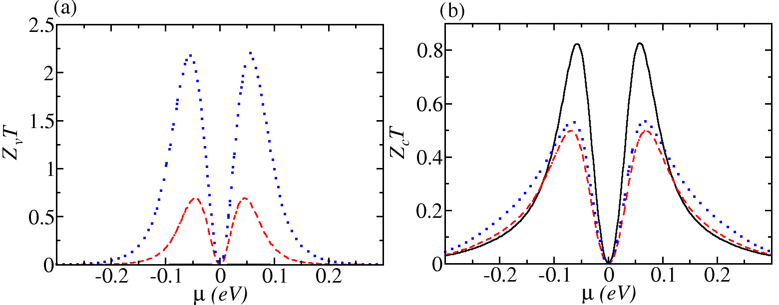
The variation of the valley and charge figures of merit and with are shown in Fig. (8a) and Fig. (8b) respectively for different values of .
(a) Dependence on chemical potential: Both the figures of merit show similar behavior as a function of and have maxima close to eV. The occurrence of maxima can be explained as follows – From the definition of , we see that varies as . Since and attain extrema near eV [see III.2(a)], and are also peaked around those values for the given set of parameters. The positions of the peaks are almost insensitive to the gap parameter .
(b) Dependence on gap parameter: Increase in enhances , because mainly varies as which shows increasing trend with . For , as the valley thermopower vanishes. The charge figure of merit behaves non monotonically with for eV, while for eV it increases with , thereby depicting the trend of . For eV, the decreases with (for ), becomes minimum at and starts to increase again for .
It is observed that both and get reduced with increase in . This is attributed to the fact that increase in reduces the thermopower (see III.2) while the ratio of and does not vary appreciably with . For the parameters used in the problem, the maximum values of and are 2.2 and 0.82 respectively. With the inclusion of phonon’s thermal conductance using the value in Ref. [66], and are reduced to and respectively. However, the value mentioned in the Ref. [66] is for pristine borophene, whereas our system is a hetero-junction with a band gap in the dispersion of middle region. Thus the values are not accurate, rather an estimation.
Here we would like to mention that the structure of borophene is anisotripic along and directions and it affects on the transport properties in two directions differently. For bulk borophene cases in Ref. [35], the electrical and thermal conductance in two directions differ quantitatively rather than qualitatively, while the results obtained for thermopower and figure of merit are almost direction independent. Since the results in both directions are qualitatively same, we have presented the results for isotropic case.
IV Conclusion
We propose a graphene/gapped tilted Dirac material/graphene junction which may exhibit valley Seebeck effect when the middle region is irradiated with off-resonant circularly polarized light. The effect arises due to unequal gaps at the two valleys caused by the combination of Semenoff mass and photoinduced mass , where is the valley index. Valley polarized thermoelectric properties arise in the device owing to unequal transmission probabilities in the conducting channels of the non-degenerate valleys. We have studied the valley caloritronics of this junction device in a systematic framework and compared the results with the corresponding charge caloritronics. In particular, we have studied the dependence of chemical potential and the role of a tunable gap parameter in the electrical and thermal conductances, Seebeck coefficient (thermopower) and figure of merit of this junction. Since the the renormalized radiation amplitude under off-resonant approximation (see Appendix A), the contributions from non-zero order Floquet sidebands in the transport properties of the system have been neglected.
The valley polarized electrical conductance attains a maximum and then decreases asymptotically to zero while the total charge conductance increases monotonically with chemical potential (). Furthermore, increases with for and decreases with for , while shows a decreasing trend with . The electrical thermal conductance as a function of and shows almost similar behavior as charge conductance, as it proportional to the amount of heat energy carried by the charge carriers. Both valley () and charge Seebeck coefficients () attain maximum values at eV which is roughly independent of . But, increases with , while shows non-monotonic nature for eV. For eV, the shows minimum values at and starts to gain weight as we decrease (for ) or increase (for ). For eV, an increase in leads to a small enhancement in .
Since the ratio of and does not show any significant change with , the figure of merit as a function of shows a variation similar to square of thermopower and its maximum value is obtained at eV. We have also analyzed the effect of tilting in the thermoelectric properties. The tilt parameter reduces the effective transmission through the junction, thereby diminishing all the charge and valley polarized quantities.
The exploitation of valley thermoemf for thermoelectric power generation may serve as a new development in the field of valley caloritronics. Since the photoinduced mass and Semenoff mass can be adjusted by varying the intensity of the light source and the strength of inversion symmetry-breaking electric field respectively, the tuning of the gap parameter may be achievable in an experimental setup.
ACKNOWLEDGEMENTS
P. Kapri thanks Department of Physics, IIT Kanpur, India for financial support.
Appendix A Floquet Hamiltonian of a tilted Dirac material subjected to circularly polarized radiation
The Hamiltonian for quasiparticles with massive tilted anisotropic Dirac dispersion in the vicinity of two independent Dirac points in materials like borophene or quinoid graphene is given by [27, 28, 29, 37]
| (15) |
where , are the Pauli matrices, is the identity matrix and denotes the two independent Dirac points. is the mass term due to different onsite energies of the two sublattices. The energy dispersion and the corresponding wave functions associated with the Hamiltonian in Eq. (15) are given by
| (16) |
and
| (17) |
where , and and denotes the conduction and valence bands, respectively. Note that term tilts the Dirac spectrum and is responsible for the electron-hole symmetry breaking, even for case.
Considering the borophene sheet is illuminated normally by intense circularly polarized electromagnetic radiation. The vector potential corresponding to the circularly polarized radiation is given by , where with being the amplitude of the electric field vector and is the frequency of the radiation. The vector potential is time-periodic since , with the time-period .
The time-periodic Hamiltonian in presence of the electromagnetic radiation is given by
| (18) |
where with . It is known that a gap in the Dirac spectrum can be induced in graphene, on the surface states of topological insulator, silicene, semi-Dirac systems, MoS2 etc by off-resonant radiation. The off-resonant condition is achieved when the photon energy () is much higher than the band width (6 with being the nearest-neighbor hopping energy) of the undriven borophene. In the off-resonant condition, the band structure is modified by the second-order virtual photon absorption-emission processes. The effective time-independent Floquet Hamiltonian in the off-resonant limit can be expressed as [67, 68, 69]
| (19) |
where the terms in the commutator are the Fourier components of ,
| (20) |
Using Eq. (20) we find the commutator as given below,
| (21) |
where is the gap at the Dirac points, an experimentally tunable parameter. The gap parameter does not depend on the tilt parameter .
Here, we would like to mention that the scattering by the Floquet side bands are neglected in our study due to the off-resonant condition of light. For off-resonant light, the th () order Floquet sidebands are separated from zeroth order bands (static modes) by large quasienergies (). As discussed in [54], the inelastic scatterings, i.e., photon absorptions and emissions between the sidebands are suppressed by a factor of , where is the renormalized radiation amplitude, with being the lattice constant. Also, the transmission coefficients for sidebands of order are small (. In our system, the value of for the chosen parameters to evaluate is . Thus, the modification in transmission probability due to the scattering by the Floquet side bands is negligibly small.
Appendix B Transmission probability
In this appendix, we provide the derivation of the transmission probability of the electron along with some plots of transmission probability (as a function of incident angle) which are required to justify the results presented in Figs. (3) and (4).
The wave functions in the three different regions, , and will have the same -dependence: with . The wave functions, , and for the three different regions for and sublattices can be written in the following forms: for ,
| (26) |
for
| (31) |
and for
| (34) |
Here the expression for is given by
| (35) |
The valley dependent reflection amplitude and the transmission amplitude are obtained by matching the wave functions at the interfaces and :
| (36) |
From the above conditions, the valley-dependent transmission probability is obtained as
| (37) |
Here, it should be noted that there is no mechanism present in the junction that mixes states of opposite valleys. The system can be reduced to a gapless single graphene sheet by setting and . In this limiting case, it can be easily checked that .
To understand the behavior of (Figs. (3) and (4)), plots for for different conditions as a function of the incident angle for a fixed energy eV and nm are shown in Figs. (9), (10) and (11).
Figures (9) and (10) show plots of as a function of for and for two values of with fixed at eV. On the other hand, Fig. (11) shows plot of as a function of for . All the figures show that the transmission probability is close to unity around the normal incidence () for both the valleys. This is manifestation of perfect tunneling when incident wave vector is normal to the interface.
Figure (9) shows that the transmission is allowed over the full range of incident angle (), whereas for Fig. (10), the transmission is restricted below the lower critical angle and above the upper critical angle. Further, in Fig. (11), the transmission probability for ceases to zero above/below some critical incident angles. This is because of , as shown in the inset of the Fig. (11), for which above or below the critical angles the wave vector in the middle region becomes complex which leads to evanescent wave. Figures (10) and (11) reveal that the allowed range of incident angle for is bigger than that of the , as for the latter one, the band gap is wider. It it is clear that the value of critical angles depend on all the three velocities , and . Similar critical angles exist in other semiconductor junction devices [70, 71].
Appendix C Theory of Thermoelectricity
In this appendix, we present the derivation of thermopower and electron’s thermal conductance in terms of the transmission probability.
Assuming that the graphene leads are independent electron reservoirs, the chemical potential and the temperature of the left/right graphene leads are and , respectively. The population of electrons at the left/right leads is described by the Fermi-Dirac distribution function . Employing the Landauer-Buttiker formalism in quasi-ballistic regime, the valley-dependent charge current is given by
| (38) |
where is the energy dependent number of transverse modes in the graphene sheet of width [72]. Here it has been used that with is the transmission probability of an electron with energy and incidence angle from left (right) graphene leads.
In absence of any external bias voltage , the chemical potentials of the two leads are taken to be the same as . Due to the applied temperature difference between the two leads, there will be a small voltage difference between the leads. The currents induced by and are given by and , where the currents and can be calculated from Eq. (38). Since in an open circuit condition, the current cannot flow, one can write
| (39) |
Expanding the Fermi-Dirac distribution functions in Eq. (38) and Eq. (39) in the linear response regime, i.e., up to the first order terms in and , one can get the valley resolved Seebeck coefficient as
| (40) |
where the kinetic coefficients for the quasi-ballistic transport regime are given by
| (41) |
with .
The flow of electrons can also transport thermal energy through the junction, which is responsible for the thermal current. The electron’s thermal current is the energy current carried by electrons traveling between leads driven by and . Analogous to the charge current, the electron’s valley resolved thermal current can be written as
Analogous to the charge current driven by and , the electron’s valley resolved thermal current can be written as
| (43) |
where and . Note that is generated by the Seebeck effect due to the temperature difference . Both and can be calculated using Eq. (C). Similarly, the electron’s thermal conductance, has two components:
| (44) |
where and are the portions of the electron’s thermal conductance driven by and respectively. The electron’s valley resolved thermal conductance can be expressed in terms of the kinetic coefficients (as given in 41) [59, 60] as
| (45) |
References
- [1] L. D. Hicks and M. S. Dresselhaus, Phys. Rev. B, 47, 12727 (1993).
- [2] L. D. Hicks and M. S. Dresselhaus, Phys. Rev. B 47, 16631 (1993).
- [3] R. Venkatasubramanian, E. Siivola, T. Colpitts, and B. O’Quinn, Nature (London) 413, 597 (2001).
- [4] R. Arita, K. Kuroki, K. Held, A. V. Lukoyanov, S. Skornyakov, and V. I. Anisimov, Phys. Rev. B 78, 115121 (2008).
- [5] N. Hamada, T. Imai, and H. Funashima, J. Phys.: Condens. Matter 19, 365221 (2007).
- [6] J. M. O. Zide, D. Vashaee, Z. X. Bian, G. Zeng, J. E. Bowers, A. Shakouri, and A. C. Gossard, Phys. Rev. B 74, 205335 (2006).
- [7] P. Wei, W. Bao, Y. Pu, C. N. Lau, and J. Shi, Phys. Rev. Lett. 102, 166808 (2009).
- [8] Y. M. Zuev, W. Chang, and P. Kim, Phys. Rev. Lett. 102, 096807 (2009).
- [9] T. Kato, S. Usui, and T. Yamamoto, Jpn. J. Appl. Phys. 52, 06GD05 (2013).
- [10] M. Buscema, M. Barkelid, V. Zwiller, H. S. J. van der Zant, G. A. Steele, and A. Castellanos-Gomez, Nano Lett. 13, 358 (2013).
- [11] S. Konabe and T. Yamamoto, Phys. Rev. B 90, 075430 (2014).
- [12] L. D. Hicks, T. C. Harman, X. Sun, and M. S. Dresselhaus, Phys. Rev. B 53, R10493(R) (1996).
- [13] M. S. Dresselhaus, G. Chen, M. Y. Tang, R. Yang, H. Lee, D. Wang, Z. Ren, J.-P. Fleurial, and P. Gogna, Adv. Mater. 19, 1043 (2007).
- [14] D. Bilc, S. D. Mahanti, K. F. Hsu, E. Quarez, R. Pcionek, and M. G. Kanatzidis, Phys. Rev. Lett. 93, 146403 (2004).
- [15] J. P. Heremans, V. Jovovic, E. S. Toberer, A. Saramat, K. Kurosaki, A. Charoenphakdee, S. Yamanaka, and G. J. Snyder, Science 321, 554 (2008).
- [16] W.-S. Liu, L.-D. Zhao, B.-P. Zhang, H.-L. Zhang, and J.-F. Li, Appl. Phys. Lett. 93, 042109 (2008).
- [17] M. Markov, X. Hu, H.-C. Liu, N. Liu, S. J. Poon, K. Esfarjani, and M. Zebarjadi, Sci. Rep. 8, 9876 (2018).
- [18] A. K. Geim and K. S. Novoselov, Nat. Mater. 6, 183191 (2007).
- [19] D. Pesin and A. H. MacDonald, Nature Materials 11, 409 (2012).
- [20] B. Feng, H. Li, C. Liu, T. Shao, P. Cheng, Y. Yao, S. Meng, L. Chen, and K. Wu, ACS Nano, 7 (10), 9049 (2013).
- [21] R. Quhe, Y. Yuan, J. Zheng, Y. Wang, Z. Ni, J. Shi, D. Yu, J. Yang, and J. Lu, Sci. Rep. 4, 5476 (2014).
- [22] K. F. Mak, C. Lee, J. Hone, J. Shan, and T. F. Heinz, Phys. Rev. Lett. 105, 136805 (2010).
- [23] A. J. Mannix, X. F. Zhou, B. Kiraly, J. D. Wood, D. Alducin, B. D. Myers, X. Liu, B. L. Fisher, U. Santiago, J. R. Guest, M. J. Yacaman, A. Ponce, A. R. Oganov, M. C. Hersam, and N. P. Guisinger, Science 350, 1513 (2015).
- [24] L. Xu, A. Du, and L. Kou, Phys. Chem. Chem. Phys. 18, 27284 (2016).
- [25] X. F. Zhou, X. Dong, A. R. Oganov, Q. Zhu, Y. Tian, and H. T. Wang, Phys. Rev. Lett 112, 085502 (2014).
- [26] A. Lopez-Bezanilla and P. B. Littlewood, Phys. Rev. B 93, 241405(R) (2016).
- [27] A. Zabolotskiy and Y. Lozovik, Phys. Rev. B 94, 165403 (2016).
- [28] M. Nakhaee, S A Ketabi, and F M Peeters, Phys. Rev. B 97, 125424 (2018).
- [29] M. O. Goerbig, Rev. Mod. Phys. 83, 1193 (2011).
- [30] M. O. Goerbig, J.-N. Fuchs, G. Montambaux, and F. Piéchon Phys. Rev. B 78, 045415 (2008).
- [31] S. Verma, A. Mawrie, and T. K. Ghosh, Phys. Rev. B 96, 155418 (2017).
- [32] SK F. Islam and A. M. Jayanavar, Phys. Rev. B 96, 235405 (2017).
- [33] Z. Jalali-Mola and S. A. Jafari, Phys. Rev. B 98, 195415 (2018).
- [34] A. E. Champo and G. G. Naumis, Phys. Rev. B 99, 035415 (2019).
- [35] M. Zare, Phys. Rev. B 99, 235413 (2019).
- [36] B. Feng, O. Sugino, R.-Y. Liu, J. Zhang, R. Yukawa, M. Kawamura, T. Iimori, H. Kim, Y. Hasegawa, H. Li et al., Phys. Rev. Lett. 118, 096401 (2017).
- [37] M. Ezawa, Phys. Rev. B 96, 035425 (2017).
- [38] X. Liu and M. C. Hersam, Sci. Adv. 5, 6444 (2019).
- [39] L. Zhang, K. Gong, J. Chen, L. Liu, Y. Zhu, D. Xiao, and H. Guo, Phys. Rev. B 90, 195428 (2014).
- [40] J. Wang, K. S. Chan, and Z. Lin, Appl. Phys. Lett. 104, 013105 (2014).
- [41] Z. P. Niu and S. Dong, Appl. Phys. Lett. 104, 202401 (2014).
- [42] X. Chen, L. Zhang, and H. Guo, Phys. Rev. B 92, 155427 (2015).
- [43] K. Uchida, S. takahasi, K. Harii, J. Ieda, W. Koshibae, K. Ando, S. Maekawa, and S Saitoh, Nature (London) 455, 778 (2008).
- [44] C. M. Jaowrski, J. Yang Smack, D. D. Awschalom, J. P. Heremans, and R. C. Myers, Nat. Mater. 9, 898 (2010).
- [45] G. E. W. Bauer, A. H. macdonald, S. Maekawa, Solid State Commun. 150, 459 (2010).
- [46] G. E. W. Bauer, E. Saitoh, and B. J. Wees, Nat. Mater., 11, 391, (2012).
- [47] M. Hatami, G. E. W. Bauer, Q. F. Zhang, and P. J. Kelly, Phys. Rev. B, 79, 174426, (2009).
- [48] X. B. Chen, Y. Z. Liu, B. L. Gu, W. H. Duan, and F. Liu, Phys. Rev. B, Phys. Rev. B, 90, 121403, (2014).
- [49] W. Yao, D. Xiao, and Q. Niu, Phys. Rev. B 77, 235406 (2008).
- [50] T. Cao, G. Wang, W. Han, H. Ye, C. Jhu, J. Shi, Q. Niu, P. Tan, E. Wang, B. Liu, and J. Feng, Nat. Commun. 3, 887 (2012).
- [51] Y. J. Zhang, T. Oka, R. Suzuki, J. T. Ye, and Y. Iwasa, Science 344, 725 (2014).
- [52] K. F. Mak, K. L. McGill, J. Park, and P. L. McEuen, Science, 344, 1489 (2014).
- [53] P. Sengupta, Y. Tan, E. Bellotti, and J. Shi, J. Phys.: Condens. Matter 30, 435701 (2018).
- [54] T. Kitagawa, T. Oka, A. Brataas, L. Fu, and E. Demler Phys. Rev. B 84, 235108 (2011).
- [55] F. D. M. Haldane, Phys. Rev. Lett. 61, 2015 (1988).
- [56] J. Jung, A. M. DaSilva, A. H. MacDonald, and S. Adam, Nat. Commun. 6, 6308 (2015).
- [57] X. Cao, J. Shi, M. Zhang, X. Jiang, H. Zhong, P. Huang, Y. Ding, and M. Wu, J. Phys. Chem. C 120, 11299 (2016).
- [58] R. Takahashi and S. Murakami, Phys. Rev. B 81, 161302 (2010).
- [59] A. Mawrie and B. Muralidharan, Phys. Rev. B 100, 081403(R) (2019).
- [60] Y. S. Liu, B. C. Hsu, and Y. C. Chen, J. Phys. Chem, 115, 6111, (2011).
- [61] R. Swirkowicz, M. Wierzbicki, and J. Barana, Phys. Rev. B, 80, 195409, (2009).
- [62] M. Wierzbicki, R. Swirkowicz, and J. Barnas Phys. Rev. B, 88, 235434 (2013).
- [63] B. Z. Rameshti and A. G. Moghaddam Phys. Rev. B, 91, 155407 (2015).
- [64] T. Tohei, A. Kuwabara, F. Oba, and I. Tanaka, Phys. Rev. B 73, 064304 (2006).
- [65] H. Zhou, Y. Cai, G. Zhang, and Y.-W. Zhang, npj. 2D Mater. Appl. 1, 14 (2017).
- [66] H. Xiao, W. Cao, T. Ouyang, S. Guo, C. He, and J. Zhong Sci. Rep. 7, 45986 (2017).
- [67] W. Magnus, Commun. Pure Appl. Math. 7, 649 (1954).
- [68] S. Blanes, F. Casas, J. A. Oteo, and J. Ros, Phys. Rep. 470, 151 (2009).
- [69] A. Lopez, A. Scholz, B. Santos, and J. Schliemann, Phys. Rev. B 91, 125105 (2015).
- [70] M. Khodas, A. Shekhter, and A. M. Finkelstein, Phys. Rev. Lett. 92, 086602 (2004).
- [71] M. I. Alomar and D. Sanchez, Phys. Rev. B 89, 115422 (2014).
- [72] C. W. J. Beenakker, Phys. Rev. Lett. 97, 067007 (2006).