Experimental evidence of monolayer AlB2 with symmetry-protected Dirac cones
Abstract
Monolayer AlB2 is composed of two atomic layers: honeycomb borophene and triangular aluminum. In contrast with the bulk phase, monolayer AlB2 is predicted to be a superconductor with a high critical temperature. Here, we demonstrate that monolayer AlB2 can be synthesized on Al(111) via molecular beam epitaxy. Our theoretical calculations revealed that the monolayer AlB2 hosts several Dirac cones along the –M and –K directions; these Dirac cones are protected by crystal symmetries and are thus resistant to external perturbations. The extraordinary electronic structure of the monolayer AlB2 was confirmed via angle-resolved photoemission spectroscopy measurements. These results are likely to stimulate further research interest to explore the exotic properties arising from the interplay of Dirac fermions and superconductivity in two-dimensional materials.
The discovery of the high-temperature superconductor MgB2 ( 39 K) has stimulated significant research interest in the AlB2-family of materials KangWN2001 ; NagamatsuJ2001 . In MgB2, the -bonding boron orbitals couple strongly with the in-plane B-B stretching phonon modes BohnenKP2001 ; YildirimT2001 ; KongY2001 ; ChoiHJ2002 , which is crucial for the occurrence of high-temperature superconductivity. However, in AlB2, an isostructural compound of MgB2, the boron state is located far below the Fermi level and lacks effective coupling with phonons in the boron layer BohnenKP2001 ; MedvedevaNI2001 . Therefore, no experimental evidence for AlB2 superconductivity has been reported to date. Recently, the desire to miniaturize quantum devices has driven significant research interest in two-dimensional (2D) materials CastroNeto2009 ; XuM2013 . In the 2D limit, monolayer AlB2 has been predicted to be a superconductor with intriguing multigap character GaoM2019 ; ZhaoY2019 , which is in stark contrast with the non-superconducting properties of bulk AlB2. In addition, bulk AlB2 has been found to host Dirac nodal lines TakaneD2018 , which indicates the possible existence of topological band structures in monolayer AlB2. However, the synthesis of monolayer AlB2 has remained a challenge to date and little is known about the topological properties of monolayer AlB2.
Recently, various synthetic 2D materials have been realized via molecular beam epitaxy (MBE), including silicene VogtP2012 ; FengB2012 , stanene ZhuF2015 ; DengJ2018 , and borophene MannixAJ2015 ; FengB2016 . In particular, honeycomb borophene, an important constituent of monolayer AlB2, has been realized on Al(111) LiW2018 . Notably, the topmost atomic layer of Al(111) has a flat triangular lattice that can constitute monolayer AlB2 with honeycomb borophene. However, in the previously proposed structure model, the lattice of borophene was compressed to fit the lattice constant of Al(111) LiW2018 ; ZhuL2019 ; GaoM2019 , and thus the topmost triangular Al lattice was inseparable from the underlying Al(111) substrate. This results in strong hybridization of the electronic structure of AlB2 with the substrate.
In this work, however, our combined low-energy electron diffraction (LEED) and scanning tunneling microscopy (STM) measurements show that the lattice constant of the surface AlB2 layer is slightly larger than that of Al(111) (Fig. 1(a)-1(d)), which indicates relatively weak coupling between AlB2 and Al(111). We also studied the electronic structures and topological properties of monolayer AlB2 via angle-resolved photoemission spectroscopy (ARPES) and first-principles calculations. Several symmetry-protected Dirac cones were observed in a freestanding AlB2 monolayer, and most of them were preserved on Al(111). Moreover, some of the Dirac bands cross the Fermi level and may contribute to electron-phonon coupling. Therefore, the realization of monolayer AlB2 provides an ideal platform to study the exotic properties that arise from the coexistence of Dirac fermions and superconductivity.
The sample preparation, transfer, and measurements were all performed in ultrahigh vacuum systems with a base pressure lower than 1.010-8 Pa. A clean Al(111) substrate was prepared via repeated sputtering and annealing cycles. Pure boron (99.9999%) was evaporated onto Al(111) using an e-beam evaporator. The Al(111) substrate was held at a temperature of 500 K during growth. The STM experiments were performed in a home-built low-temperature STM-MBE system and the data was acquired at 78 K. The LEED and ARPES measurements were performed at the BL-1 IwasawaH2017 and BL-9A of the Hiroshima synchrotron radiation center. The energy resolution of the ARPES measurements was 15 meV; the temperature of the sample during both the ARPES and LEED measurements was maintained at 30 K.
First-principles calculations were performed using the Vienna ab initio simulation package (VASP) KresseJ1993 based on the generalized gradient approximation (GGA) Blochl1994 in the Perdew-Burke-Ernzerhof (PBE) functional PerdewJP1997 and the projector augmented-wave (PAW) pseudopotential MonkhorstHJ1976 . The energy cutoff was set to 400 eV for the plane-wave basis and the Brillouin Zone was sampled using a centered Monkhorst-Pack grid PerdewJP1992 (18181). The vacuum space was set to be larger than 20 Å. All the atomic positions and lattice parameters were fully relaxed before further calculations, and the maximum force allowed on each atom was less than 0.01 eV Å-1. The numerical convergence accuracy of the total energy was 110-6 eV per cell. Spin-orbit coupling (SOC) effects were neglected in all our calculations. The first-principles phonon calculations were implemented in VASP and PHONOPY TogoA2015 within the framework of the density functional perturbation theory (DFPT) GonzeX1997 ; GiannozziP1991 .
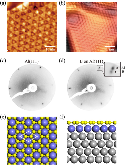
The growth of boron on Al(111) leads to the formation of an ordered structure with triangular corrugations, as shown in Fig. 1(a). The period of the triangular corrugation is 7 nm. From the high-resolution STM image in Fig. 1(b), a honeycomb-like structure can be observed with a lattice constant of 3.0 Å, which indicates the formation of the honeycomb borophene. These results agree well with previous reports LiW2018 . LEED measurements were performed to study the atomic structure of this system. Figure 1(c) and 1(d) show the LEED patterns of pristine Al(111) and B/Al(111), respectively. It was found that the lattice constant of the surface structure was slightly larger than that of Al(111), as shown in the inset of Fig. 1(d). Based on the LEED pattern, the lattice constant of the surface structure was estimated to be 2.98 Å, which was in qualitative agreement with the STM results. Because of the different lattice constants of the surface structure and the underlying substrate, moiré patterns form because of the lattice mismatch. A simple analysis shows that the 2525 superstructure of Al(111) (=2.86 Å) corresponds to the 2424 superstructure of the surface layer (=2.98 Å). The period of the superstructure is 7.15 nm, which is in agreement with the period of the triangular corrugations (7 nm). Therefore, our results confirmed that the triangular corrugations originate from the moiré patterns of the system.
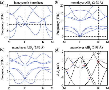
There are two possibilities for the atomic structure of the surface layer: (1) only honeycomb borophene; (2) two atomic layers that contain the topmost borophene and a triangular Al, i.e., monolayer AlB2. First-principles calculations were performed to confirm the correct structure model. The optimized lattice constants of the freestanding borophene and AlB2 are 2.92 Å and 2.98 Å, respectively. The calculated lattice constants of the freestanding AlB2 monolayer were in excellent agreement with our experimental values. Figure 2(a) and 2(b) show the phonon spectrum of the freestanding honeycomb borophene and monolayer AlB2. A significant imaginary frequency component can be observed for the honeycomb borophene, while no imaginary frequencies were observed for the monolayer AlB2, which indicates that the monolayer AlB2 is more stable than the honeycomb borophene. In addition, the monolayer AlB2 will become unstable if the lattice constant is reduced to fit Al(111) (=2.86 Å), as shown in Fig. 2(c). Therefore, for the B/Al(111) system, we can conclude that the monolayer AlB2 as a whole has a larger lattice constant than Al(111). The lattice mismatch and appearance of moiré patterns indicate a relatively weak interaction of the monolayer AlB2 with the Al(111) substrate.
After establishing the synthesis of the AlB2 monolayer, we move on to studying its electronic structure. Figure 2(d) shows the calculated band structure of freestanding AlB2, which is in agreement with recent calculation results ZhaoY2019 . In proximity to the point, there are several bands that cross the Fermi level: , , and . Interestingly, these bands host two Dirac cones along the –K and –M directions, respectively, as indicated by the red arrows in Fig. 2(d). The mirror eigenvalues of these bands are indicated by the “+” and “-” signs. The crossing bands of these Dirac cones have opposite eigenvalues, which indicates that these Dirac cones are protected by the mirror reflection symmetry: the –K– plane and –M– plane, respectively. Another Dirac cone is centered at the K point, as indicated by the red circle in Fig. 2(d). This Dirac cone derives from the orbitals of boron SM , analogous to the Dirac cone of the honeycomb lattice. Therefore, the Dirac cone at the K point originates from the honeycomb borophene and survives in the monolayer AlB2 despite the inclusion of a hexagonal Al layer.
According to the previous calculations, coupling between the boron bands (i.e., , and bands in our work) and the in-plane phonon modes gives rise to superconductivity in the AlB2 monolayer GaoM2019 ; ZhaoY2019 . From our calculation results, some of the Dirac bands originate from the and bands and cross the Fermi level. Therefore, the AlB2 monolayer may have exotic properties that arise from the interplay of Dirac fermions and superconductivity.
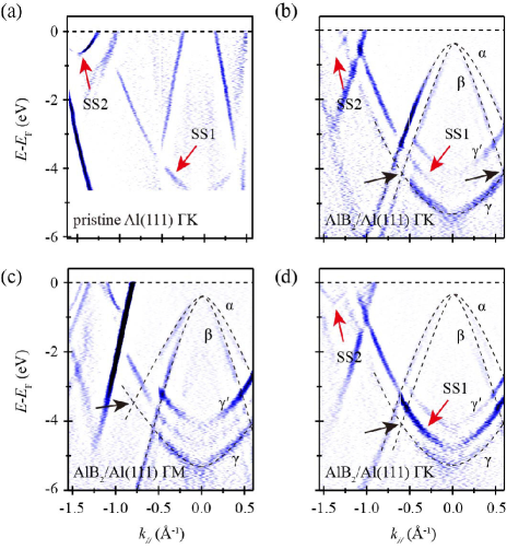
ARPES measurements were performed to verify the intriguing electronic structures of the monolayer AlB2 and the results are shown in Fig. 3. The , , and bands near the point of freestanding AlB2 can be clearly observed in the ARPES results. In particular, the Dirac cones survive without any obvious gap opening, as indicated by the black arrows. The persistence of these bands on Al(111) indicates a weak interaction between AlB2 and Al(111). There was no discernable dispersion on changing the incident photon energy, which agrees with the 2D character of these bands. Furthermore, an additional band was observed, which was located 0.5 eV above the band. This band originates from the hybridization of AlB2 with Al(111) and will be discussed later. It should be noted that two electron-like bands were observed at the and points of Al(111), as indicated by the red arrows. These bands originate from the surface states of Al(111) KevanSD1985 because the coverage of AlB2 was less than one monolayer. The observation of the Al(111) surface state indicates the high order and cleanliness of the sample surface.
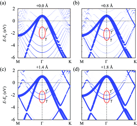
Next, the origin of the band is discussed. To this end, we performed first-principles calculations including the Al(111) substrate. Because of the large unit cell of the moiré pattern (7 nm), calculating the supercell is difficult. To simplify the calculations, the lattice constant of AlB2 was compressed from 2.98 Å to 2.86 Å to accommodate the hexagonal lattice of Al(111). The calculated band structure is shown in Fig. 4(a). It is clear that the and bands are preserved on Al(111). The band is blurred by the quantum well states arising from the finite thickness of the slab in the calculations. To distinguish the band, the distance between the AlB2 layer and Al(111) was increased to weaken the interaction of AlB2 and the substrate. This is reasonable because the simplification in our calculation inevitably increased the coupling between AlB2 and Al(111). Figures 4(b)-4(d) show the calculated band structures with different additional separations: 0.8 Å, 1.4 Å, and 1.8 Å. We find that the and bands become more prominent with increasing separation, as highlighted by the red ellipses. When the separation was further increased, the intensity of the band gradually decreased on the surface AlB2 layer and finally disappeared. In contrast, the intensity of the band gradually increased on the Al(111) substrate SM . These results indicate that the band is a hybridized state with a strong bulk character.
Our results support the formation of monolayer AlB2 on Al(111), and more importantly, the band hybridization of AlB2 and the Al(111) substrate is relatively weak. Therefore, most of the bands of the freestanding AlB2 survive on Al(111). Monolayer AlB2 has been predicted to be a superconductor with intriguing multigap character, hence, its successful synthesis in this work and the discovery of Dirac cones provides an ideal platform for studying the interplay of Dirac fermions and Bogoliugov quasiparticles in the 2D limit. It should be noted that the Al(111) substrate is also a superconductor ( 1.2 K), which could possibly ensure the persistence of superconductivity in the AlB2/Al(111) system.
Acknowledgements.
This work was supported by the Ministry of Science and Tachnology of China (Grant No. 2018YFE0202700, No. 2016YFA0300904 No. 2016YFA0300600), the National Natural Science Foundation of China (Grants No. 11974391, No. 11825405, No. 1192780039, No. 11761141013, and No. 11734003), the Beijing Natural Science Foundation (Grant No. Z180007), and the Strategic Priority Research Program of Chinese Academy of Sciences (Grant No. XDB30000000). The ARPES measurements were performed with the approval of the Proposal Assessing Committee of Hiroshima Synchrotron Radiation Center (Proposal Numbers: 19AG005 and 19AG058).References
- (1) W. N. Kang, H.-J. Kim, E.-M. Choi, C. U. Jung, and S.-I. Lee, Science 292, 1521 (2001).
- (2) J. Nagamatsu, N. Nakagawa, T. Muranaka, Y. Zenitani, and J. Akimitsu, Nature 410, 63 (2001).
- (3) K.-P. Bohnen, R. Heid, and B. Renker, Phys. Rev. Lett. 86, 5771 (2001).
- (4) T. Yildirim, O. Gülseren, J. W. Lynn, C. M. Brown, T. J. Udovic, Q. Huang, N. Rogado, K. A. Regan, M. A. Hayward, J. S. Slusky, T. He, M. K. Haas, P. Khalifah, K. Inumaru, and R. J. Cava, Phys. Rev. Lett. 87, 037001 (2001).
- (5) Y. Kong, O. V. Dolgov, O. Jepsen, and O. K. Andersen, Phys. Rev. B 64, 020501(R) (2001).
- (6) H. J. Choi, D. Roundy, H. Sun, M. L. Cohen, and S. G. Louie, Nature 418, 758 (2002).
- (7) N. I. Medvedeva, A. L. Ivanovskii, J. E. Medvedeva, and A. J. Freeman, Phys. Rev. B 64, 020502(R) (2001).
- (8) A. H. Castro Neto, F. Guinea, N. M. R. Peres, K. S. Novoselov, and A. K. Geim, Rev. Mod. Phys. 81, 109 (2009).
- (9) M. Xu, T. Liang, M. Shi, and H. Chen, Chem. Rev. 113, 3766 (2013).
- (10) M. Gao, X.-W. Yan, J. Wang, Z.-Y. Lu, and T. Xiang, Phys. Rev. B 100, 024503 (2019).
- (11) Y. Zhao, C. Lian, S. Zeng, Z. Dai, S. Meng, and J. Ni, Phys. Rev. B 100, 094516 (2019).
- (12) D. Takane, S. Souma, K. Nakayama, T. Nakamura, H. Oinuma, K. Hori, K. Horiba, H. Kumigashira, N. Kimura, T. Takahashi, and T. Sato, Phys. Rev. B 98, 041105(R) (2018).
- (13) P. Vogt, P. De Padova, C. Quaresima, J. Avila, E. Frantzeskakis, M. C. Asensio, A. Resta, B. Ealet, and G. LeLay, Phys. Rev. Lett. 108, 155501 (2012).
- (14) B. Feng, Z. Ding, S. Meng, Y. Yao, X. He, P. Cheng, L. Chen, and K. Wu, Nano Lett. 12, 3507 (2012).
- (15) F.-f. Zhu, W.-j. Chen, Yo. Xu, C.-l. Gao, D.-d. Guan, C.-h. Liu, D. Qian, S.-C. Zhang, and J.-f. Jia, Nat. Mater. 14, 1020 (2015).
- (16) J. Deng, B. Xia, X. Ma, H. Chen, H. Shan, X. Zhai, B. Li, A. Zhao, Y. Xu, W. Duan, S.-C. Zhang, B. Wang, and J. G. Hou, Nat. Mater. 17, 1081 (2018).
- (17) A. J. Mannix, X.-Fe. Zhou, B. Kiraly, J. D. Wood, Diego Alducin, B. D. Myers, X. Liu, B. L. Fisher, U. Santiago, J. R. Guest, M. J. Yacaman, A. Ponce, A. R. Oganov, M. C. Hersam, and N. P. Guisinger, Science 350, 1513 (2015).
- (18) B. Feng, J. Zhang, Q. Zhong, W. Li, S. Li, H. Li, P. Cheng, S. Meng, L. Chen, and K. Wu, Nat. Chem. 8, 563 (2016).
- (19) W. Li, L. Kong, C. Chen, J. Gou, S. Sheng, W. Zhang, H. Li, L. Chen, P. Cheng, and K. Wu, Sci. Bull. 63, 282 (2018).
- (20) L. Zhu, B. Zhao, T. Zhang, G. Chen, and S. A. Yang, J. Phys. Chem. C 123, 14858 (2019).
- (21) H. Iwasawa, K. Shimada, E. F. Schwier, M. Zheng, Y. Kojima, H. Hayashi, J. Jiang, M. Higashiguchi, Y. Aiura, H. Namatame, and M. Taniguchi, J. Synchrotron Radiat. 24, 836 (2017).
- (22) G. Kresse and J. Hafner, Phys. Rev. B 47, 558(R) (1993).
- (23) P. E. Blöchl, Phys. Rev. B 50, 17953 (1994).
- (24) J. P. Perdew, K. Burke, and M. Ernzerhof, Phys. Rev. Lett. 78, 1396 (1997).
- (25) H. J. Monkhorst and J. D. Pack, Phys. Rev. B 13, 5188 (1976).
- (26) J. P. Perdew, J. A. Chevary, S. H. Vosko, K. A. Jackson, M. R. Pederson, D. J. Singh, and C. Fiolhais, Phys. Rev. B 46, 6671 (1992).
- (27) A. Togo, and I. Tanaka, Scr. Mater. 108, 1 (2015).
- (28) X. Gonze and C. Lee. Phys. Rev. B 55, 10355 (1997).
- (29) P. Giannozzi, S. de Gironcoli, P. Pavone, and S. Baroni, Phys. Rev. B 43, 7231 (1991).
- (30) See Supplementary Material for additional calculation results.
- (31) S. D. Kevan, N. G. Stoffel, and N. V. Smith, Phys. Rev. B 31, 1788 (1985).