Hard-gap spectroscopy in a self-defined mesoscopic InAs/Al nanowire Josephson junction
Abstract
Superconductor/semiconductor-nanowire hybrid structures can serve as versatile building blocks to realize Majorana circuits or superconducting qubits based on quantized levels such as Andreev qubits. For all these applications it is essential that the superconductor-semiconductor interface is as clean as possible. Furthermore, the shape and dimensions of the superconducting electrodes needs to be precisely controlled. We fabricated self-defined InAs/Al core/shell nanowire junctions by a fully in-situ approach, which meet all these criteria. Transmission electron microscopy measurements confirm the sharp and clean interface between the nanowire and the in-situ deposited Al electrodes which were formed by means of shadow evaporation. Furthermore, we report on tunnel spectroscopy, gate and magnetic field-dependent transport measurements. The achievable short junction lengths,the observed hard-gap and the magnetic field robustness make this new hybrid structure very attractive for applications which rely on a precise control of the number of sub-gap states, like Andreev qubits or topological systems.
I Introduction
Over the last decade, superconductor-semiconductor nanowire hybrid structures have experienced growing interest as building blocks in circuits based on various novel physical phenomena. In superconducting transmon quantum bits Josephson junctions featuring a semiconductor nanowire weak link between two superconducting electrodes allow for gate control instead of flux control as employed in conventional Josephson junctions Larsen et al. (2015); de Lange et al. (2015); Casparis et al. (2016); Luthi et al. (2018). This makes the circuit layout much more compact. In addition, one can also make use of the relatively large Fermi wavelength in the semiconductor being comparable with the nanowire dimensions. As a consequence, well-distinguished quantized levels are formed, which might be used to realize an Andreev quantum bit Zazunov et al. (2003); van Woerkom et al. (2017); Tosi et al. (2019); Hays et al. (2018).
One of the most exciting properties of such nanowire-superconductor hybrid structures is the access to the mesoscopic regime, in which the behavior of the realized Josephson junction is fully-determined by the coherent bound states inside the semiconductor. Due to the presence of spin-orbit coupling in III-V semiconductor nanowires, it is also possible to observe exotic phenomena beyond the classical Andreev spectrum Gharavi and Baugh (2015); Park and Yeyati (2017); van Dam et al. (2006); van Woerkom et al. (2017); Tosi et al. (2019). After the first observation of signatures of Majorana fermions in nanowire-superconductor hybrid structures Mourik et al. (2012); Deng et al. (2012); Rokhinson et al. (2012); Zhang et al. (2017), the interest has extended towards realizing topological quantum bits Albrecht et al. (2016); Karzig et al. (2017). One reason is that owing to the non-local nature of Majorana states, topological quantum circuits are less prone to errors Alicea et al. (2010).
The performance of nanowire-based Josephson junctions depends to a large extent on the properties of the superconductor-semiconductor interface. In most cases, the superconductor is deposited ex-situ after the growth of the nanowire. This makes it necessary to carry out some surface cleaning steps, e.g. wet chemical etching or Ar+ sputtering, before superconductor deposition Gül et al. (2017). However, this procedure often results in a non-ideal interface. In order to circumvent this problem, efforts were undertaken to deposit the superconductor in-situ, i.e. without breaking the vacuum after the growth of the nanowires Krogstrup et al. (2015); Chang et al. (2015); Güsken et al. (2017); Gazibegovic et al. (2017); Bjergfelt et al. (2019). Another crucial issue is the length of the weak link junction, since it determines the number of Andreev levels involved in the Josephson supercurrent. The conventional method to define a junction in an in-situ deposited superconducting shell wire has been to use electron beam lithography and wet chemical etching Larsen et al. (2015), which puts constraints on the minimum attainable junction length due to the isotropic nature of chemical etches. In order to tackle this issue, very recently, new fabrication schemes were developed where the junction length is geometrically defined by shadow evaporation Gazibegovic et al. (2017); Schüffelgen et al. (2019); Carrad et al. (2019).
We fabricated fully in-situ InAs nanowire-based Josephson junctions, which utilizes repetition shadow evaporation of Al to define the closely spaced superconducting electrodes. The structural properties of the InAs-Al core-halfshell nanowires were investigated using transmission electron microscopy. In the transport experiments, we were able to tune the junction from the fully depleted regime, i.e. Coulomb blockade, to a well-developed Josephson supercurrent range by biasing a lithographically defined bottom gate finger. Furthermore, we present voltage-driven measurements, which are sensitive to the density of states in the nanowire and the structure of the superconducting gap. Finally, we present an analysis of the junction behavior for externally applied magnetic fields parallel to the nanowire axis and out-of-plane.
II Growth and device fabrication
The fully in-situ Josephson junctions were fabricated by using the following procedure: In order to achieve adjacent Si(111) surfaces, anisotropic etching is employed with Tetramethyl ammonium hydroxide (TMAH) on a pre-patterned Si(100) substrate with arrays of 3 m squares. The resulted tilted planes have an angle of with respect to the unetched Si(100) surface. These Si(111) facets form the basis for the subsequent InAs nanowire growth by means of catalyst-free molecular beam epitaxy (MBE).
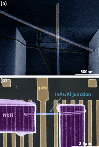
Before the NW growth, a 23 nm thick SiO2 layer is formed on the Si substrate by thermal oxidation. Then, 80 nm wide holes are defined in the oxide layer over adjacent Si(111) facets using electron beam (E-beam) lithography, reactive ion etching (RIE: CHF3+O2) and wet chemical etching (HF). The holes are positioned so that the grown NWs cross each other closely, but do not merge. The InAs NWs are grown in two steps: First, at a substrate temperature of 480C with an In growth rate of 0.08m/h (determined as the growth rate of In(100) planar layers) and an As4 beam equivalent pressure (BEP) of approx. 410mbar for 10 min to sustain an optimal growth window and then decreasing the substrate temperature to 460C with an In growth rate of 0.03m/h and an As4 BEP of approx. 310mbar for 3.5 h, resulting in 4-5m long and 80 nm wide NWs. After the growth of the InAs nanowires, the substrate undergoes an arsenic desorption at 400C for 20 min and at 450C for 5 min. By doing so, we suppress the formation of parasitic heterostructures like AlAs during the deposition of the Al, which ensures a pristine interface without any barriers. Subsequently, the sample is transferred to the metal MBE and is cooled down to C, followed by the evaporation of a 25 nm thick layer of Al onto the nanowires at this temperature Krogstrup et al. (2015); Güsken et al. (2017). During the metal evaporation process, an elevated angle of 87∘ is maintained between the metal source and the nanowire, which ensures that the metal deposition is smooth and highly crystalline. In Fig. 1(a) a scanning electron beam microscopy (SEM) image of an as-grown in-situ Al/InAs-nanowire Josephson junction with a junction length of approximately 80 nm is shown. It can be clearly seen, that the junction length is directly related to the diameter of the upper nanowire, which acts as the shadow mask.
The devices were fabricated on commercially available highly resistive Si substrates (). All etching and metal-deposition steps were realized using standard e-beam lithography techniques. At first, a single Ti/Au (5 nm/10 nm) gate electrode surrounded by a set of electrically unconnected metal stripes for mechanical support were deposited, together with a small bonding pad and a single lead between the gate and the pad. This is followed by another Ti/Au deposition (60 nm/70 nm) to form a larger bonding pad on top of the smaller one as well as additional, positive e-beam markers. The whole substrate was subsequently covered by an 3 nm/12 nm thick Al2O3/HfO2 dielectric layer by means of atomic layer deposition. As the circuits are intended to work for both AC and DC measurements, we use a transmission line to form the source contact of the device. The latter is terminated by an on-chip bias tee, consisting out of an interdigital capacitor and a planar coil. All three elements, together with the surrounding ground plane, were fabricated out of reactively sputtered titanium nitride (80 nm thick, deposited at room temperature).
Subsequently, the nanowires were then transfered onto the electrostatic gates by means of an SEM-based micro-manipulator setup. To ensure an ohmic coupling between the contacts, made out of NbTi, and the Al shell, we used a combination of a 5 s long wet chemical etch in Transene-D, followed by an in-situ Ar+ dry etch. The contact separation is chosen to be at least 1.5 m in order to reduce the effect of the wide-gap superconductor NbTi on the actual junction characteristics. Figure 1(b) shows one of the final Josephson junctions on top of a bottom gate electrode (yellow).
III Results
III.1 Structural characterisation
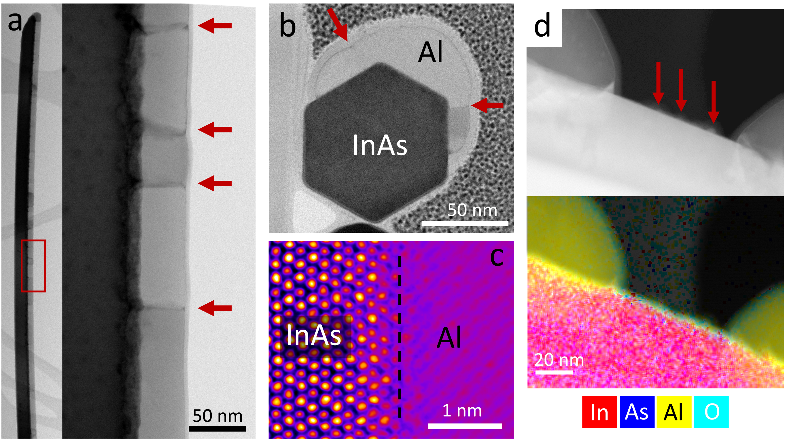
The structural properties of the InAs-Al core-half-shell nanowires were examined using scanning transmission electron microscopy (STEM). For this, the nanowires were transferred to holey carbon Cu grids by simply sweeping the arrays with the grid. The InAs nanowires grown by current catalyst-free method showed polytypic crystal structure containing thin, defective wurtzite (WZ) and zincblende (ZB) segments.
Figure 2 (a) shows a low magnification image of a core-halfshell nanowire. The Al layer is uniform along the nanowires and has a smooth surface with no significant faceting Krogstrup et al. (2015). Cross-sections prepared by focused ion beam revealed that the Al thickness is not uniform around the half-shell as shown in Fig. 2 (b). The maximum thicknesses of the Al layers in these nanowires are between 30–50 nm. The Al half-shell is formed of large grains ( nm) with different orientations. These differently oriented grains can be seen in the two viewing directions as marked by red arrows in Figs. 2 (a) and (b). Some of the observed grain orientations include and (using WZ notation for InAs). These orientations are different to those shown in some of the previous works Krogstrup et al. (2015); Kang et al. (2017); Carrad et al. (2019), but consistent with some of those seen in our prior results Güsken et al. (2017). It should also be noted that the size of the Al grains is much larger than the width of a single crystal type region in the polytypic nanowire (which is generally less than 10 mono-layers), and these grains span multiple phase changes and defects. This means that change in phase of the nanowire does not directly induce change in metal grain orientation.
The interface between the Al and InAs was analysed using the cross sections, as this viewing angle avoids simultaneous contribution to the projection from Al growth on multiple facets. Fig. 2 (c) shows a falsely colorized higher magnification image of the InAs-Al interface. It can be seen that the interface is sharp and smooth with no amorphous material in between crystalline InAs and Al, as a result of fully in-situ deposition of the electrodes and absence of processing steps such as Ar+ sputtering. Edge dislocations which have been previously attributed to AlAs formation Krogstrup et al. (2015); Güsken et al. (2017), were observed in the side view of these nanowires. Dislocations were placed nm from the interface within InAs. Evidence supporting an AlAs layer as thick as nm was not seen in energy dispersive x-ray (EDX) data or lattice spacings of high resolution images, although a smaller lattice spacing () was observed between the edge-most lattice planes in some nanowire facets, accounting to a possible AlAs or AlInAs formation of thickness less than nm. This shows that almost all of the As on the entire Nw surface has been desorbed prior to Al deposition and it is consistent with transport measurements (shown later) which show no evidence for the presence of a significant intermediate AlAs layer. Figure 2 (d) shows an annular dark field (ADF) image and the corresponding EDX map of an InAs-Al junction. A clear sharp gap in Al layer is formed in the shadowed region with a junction width of 75 nm. Few small, oxidised and isolated droplets of Al, which appears to have formed during its deposition are seen within the junction (indicated by red arrows in the ADF image). However, these seem to get etched-off during the subsequent device processing steps as no evidence of parallel metallic bypass is observed in the transport measurements.
III.2 Basic junction characteristics
All presented measurements were performed in a He3/He4 dilution refrigerator at a base temperature of 15 mK equipped with a superconducting magnet coil. traces are measured using a current bias supplied from a battery-powered current source and measured using a battery-powered differential voltage amplifier. The measurement lines within the refrigerator are heavily filtered with thermocoax, low-temperature copper powder filters and custom low pass filters in addition to room temperature ’pi’-filters.
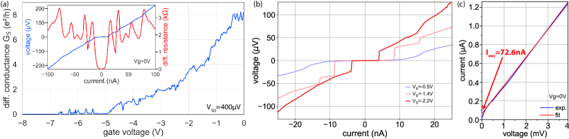
The efficiency of the gate response is one of the key properties of a nanowire junction. Therefore, we measured the conductance of the junction in a voltage-biased configuration. In Fig. 3 (a) a gate sweep for one of the in-situ devices is shown. For these measurements a constant voltage drop of 400 eV is maintained across the junction, i.e. above the induced proximity gap. Depending on the applied gate voltage , four different regimes can be distinguished. For gate voltages below V, the nanowire is completely pinched off. Above this value, the current is mediated by single electron transport through an intrinsic quantum dot. For gate voltages larger than V, the nanowire opens up, but the conductance is still limited by a low-transparency tunnel coupling to the electron reservoirs in the contacts. This results in a conductance increase of just over a gate voltage range of 2 V and just a weakly pronounced superconducting branch. For the last section, i.e. voltages above V, the current voltage () characteristics shows a classical Josephson junction response (cf. Fig. 3 (a) (inset)) with a clear supercurrent. In addition, signatures of subharmonic gap structures are found in the differential resistance Octavio et al. (1983); Flensberg et al. (1988).
Figure 3 (b) shows a set of IV curves at three different gate voltages within the Josephson-junction-regime. It can be seen, that the switching current of the device can be tuned between 3 nA and 10 nA. The additional constant-voltage-sections are related to self-induced Shapiro steps, caused by the transmission-line circuit on the sample. At we obtained a critical current of nA and a normal state resistance of , which results in an product of V. We would like to stress that the presented value just holds for the given gate voltage. Both the critical current as well as the normal state resistance are affected by quantum fluctuations, which are related to universal conductance fluctuations in the nanowire Günel et al. (2012); Doh et al. (2005). As indicated in Fig. 5(c), by extrapolating the current voltage characteristics at the normal state in the range V a finite excess current of 72.6 nA is extracted. The excess current can be used to get an estimation of the dominating type of transport within the channel by comparing the product with the superconducting gap . Following the framework of the corrected Octavio–Tinkham–Blonder–Klapwijk theory Octavio et al. (1983); Flensberg et al. (1988), we obtain a ratio of at zero gate voltage. This value can be converted to the barrier strength parameter and a corresponding contact transparency Flensberg et al. (1988); Niebler et al. (2009). This transparency is comparable to values obtained for hydrogen cleaned superconductor/nanowire junctions, i.e. Al/InSb Gazibegovic et al. (2017) or NbTiN/InSb Zhang et al. (2017).
III.3 Hard gap spectroscopy and Yu–Shiba–Rusinov states
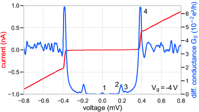
The second benchmark of a superconductor-semiconductor hybrid structure is the hardness of the induced proximity gap, i.e. the coupling strength between the nanowire and the metal shell, in the single-channel or tunneling limit. Previous experiments on similar systems used tunnel spectroscopy between one superconducting and one normal conducting contact to detect the strong change in the density of states of the device close to the gap edge Chang et al. (2015). Even though our structure is slightly different in terms of the contact setup, we can obtain comparable conditions by applying a negative gate voltage which sets the device into the tunnel-limited regime Gül et al. (2017). Figure 4 shows a typical spectroscopy-like measurement of a self-defined InAs/Al nanowire Josephson junction.
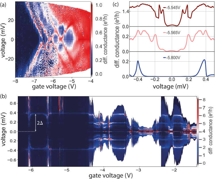
As indicated in the figure, four pronounced peaks are identified. Feature (1) is thereby related to the superconducting state, while (2) and (3) correspond to sub-gap structures. Finally, the dominating peak (4) marks the edge of the induced proximity gap 2eV. However, more important than the existence of pronounced spikes in the conductance is the ratio of the conductance for in- and out-of-gap transport, i.e. . Between (4) and (2), the conductance drops to , with a further reduction between (2) and (1) to . Such a strong decrease of the conductance is an indication that our devices host a so-called hard gap Gül et al. (2017); Chang et al. (2015); Carrad et al. (2019).
As already shown in Fig. 3, the actual junction behavior is strongly correlated with the applied gate voltage. Thus, we performed a gate batch measurement between and V in steps of mV, which covers both the tunnel-limited regime as well as the range in which the transport is dominated by multiple Andreev reflections. Figure 5 (a) shows the stability diagram of the junction for gate voltages between and V. Here, the transport is dominated by single electron tunneling, which results in pronounced Coulomb diamonds. By mapping out the size of the diamonds in terms of their individual gate and bias voltage, we obtain a lever arm and charging energy meV. Based on these values, especially due to Kiršanskas et al. (2015), we assume that the transport, in the sections in which the quantum dot is open, is mediated by Yu–Shiba–Rusinov (YSR) states rather than by conventional Andreev bound states Yu (1965); Shiba (1968); Rusinov (1969).
In order to probe the actual state structure, we performed differential conductance vs. bias voltage measurements at a high resolution gate voltage stepping in the range of to V, which is shown in Fig. 5 (b).111Compared to the measurements shown in Fig. 5 (a) the pattern is shifted slightly because of gate drift. We can distinguish between three different regimes. For less negative gate voltages, i.e. values above V, (multiple) sub-gap states arise. However, for more negative gate voltages and, especially inside of the Coulomb diamonds, the sub-gap transport is completely suppressed. Nevertheless, the edges of the induced proximity gap are still present, represented by two straight light-blue lines at a constant voltage of 375V. On the other hand, for certain gate voltage ranges, in which the quantum dot is open, several sub-gap features arise. In Fig. 5 (c) three exemplary curves in the range around V are shown. For a gate voltage of V, the junction characteristics exhibit a clear hard-gap without any sub-gap features. If the voltage increases, i.e. up to , a single state moves into the gap and additional peaks appear, which are probably related to coherent reflection events of the same state. For a gate voltage of , the state reaches zero energy, which, together with the onset of single electron tunneling, results in a 4 times increase of the in- and out-of-gap conductance as well as the emergence of a pronounced zero bias peak, probably caused by the interplay of multiple Andreev reflections and a single Yu–Shiba–Rusinov state. Based on the strong gate asymmetry, as well as due to the relatively large charging energy of , this behavior could be an indication for a quantum phase transition from a singlet into a doublet state, which effectively changes the nature of the junction from ”0” to ”” Li et al. (2017); Jørgensen et al. (2007). However, due to the fact that the junction does not carry a real, non-dissipative current in this specific gate voltage range and is not embedded in a phase-sensitive device like a superconducting quantum interference device, there is no direct way to probe the resulting reversal of the supercurrent. Nevertheless, these states could still offer some advantages for devices based on mesoscopic Josephson junctions by adding an additional energy-tunability of the states besides the superconductor-semiconductor interface transparency.
III.4 In-plane and out-of-plane magnetic field transport measurements
The common requirement for all devices based on Andreev bound states is the manipulation of the phase across the junction in order to move along the dispersion relation and set the system to a fixed operational point. This is normally achieved by means of a superconducting loop connecting the junction and applying a small external out-of-plane magnetic field which generates a flux-induced phase shift. In the case of semiconductor nanowires, and more specifically for materials like InAs or InSb, the strong spin-orbit coupling as well as the large g-factor can be used as an additional way to manipulate the state structure both in energy and momentum space. Here, an additional in-plane field is required to induce a Zeeman splitting, with field values which can easily overcome the bulk critical field of Al by one or two orders of magnitude. Both things together make the magnetic field sustainability the second key benchmark of a nanowire Josephson junction.
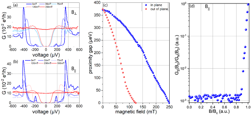
In order to probe the magnetic field stability of the in-situ junctions we performed voltage-driven measurements at a gate voltage of V, i.e. close to, but outside of the regime which is dominated by the quantum dot. Figure 6 (a) and (b) show the conductance vs. bias voltage for an out-of-plane field as well as for a magnetic field which is applied parallel to the nanowire axis, respectively.
As can be seen, both measurements show the typical damping and smearing out effect of the gap edge peaks, which is related to the continuous closing of the induced proximity gap if the magnetic field is increased. The field-induced changes in the normal-state conductance are most likely related to quantum fluctuations in the nanowire, i.e. the previously mentioned universal conductance fluctuations, induced by the superposition of multiple, flux-penetrated scattering loops. However, these should just affect the background conductance rather than the transport below the superconducting gap. By using the first derivative of the differential conductance, it is possible to extract the actual gap width for each trace. Even though this method underestimates the gap width for small magnetic fields, it makes it possible to find reliable values when the actual gap edge peaks are already completely suppressed. Figure 6 (c) summarizes the field-dependent gap width in terms of energy for both the in-plane (blue) as well as the out-of-plane (red) field. For the latter one, we obtain a critical field of mT, while the first one is almost two times larger, with mT. These comparably small values of with respect to other works can be attributed to the much thicker Al shell of 25 nm in our case Meservey and Tedrow (1971); Krogstrup et al. (2015). Additionally, both traces shown in Fig 6 (c) deviate from the conventional BCS-behaviour, resulting in a much weaker field-dependency of . However, we would like to stress that the closing of the gap is not necessarily coupled to a softening of the gap, as can be seen in Figure 6 (d). Here, we analyzed the change of the ratio between the averaged field-dependent zero bias conductance and the conductance above , , as a function of fractions of the critical field. As long as the applied in-plane field is smaller than , is mainly limited by the noise floor of the system. However, above this value, the conductance increases continuously, until it reaches . We interpret this as another proof for the hardness of the induced proximity gap in our system, which is not disturbed by parasitic sub-gap states even for comparably large magnetic fields.
IV Conclusion
We have demonstrated that mesoscopic Josephson junctions based on nanowires with shadow-mask-defined weak links show state-of-the-art properties in terms of gap-hardness, gate tunability of the switching current, interface transparency and magnetic field resilience. In fact, in contrast to conventional nanowire junctions with epitaxial Al full or half shells, they provide much more flexibility for the usable superconductors due to the avoidance of a wet or dry chemical etching step. Additionally, caused by the coupling between the actual junction length and the nanowire diameter, they ease the fabrication of short junctions, i.e. systems with just a single Andreev bound state. Thus, these novel junctions can potentially act as a building block for quantum devices based on excitations, like the Andreev qubit or topological systems with Majorana zero modes, which require a precise control of the internal state structure of the junction.
Acknowledgment
Assistance with the MBE growth by Christoph Krause is gratefully acknowledged. Dr. Stefan Trellenkamp is gratefully acknowledged for electron beam lithography. Dr. Gianluigi Catelani is gratefully acknowledged for theory support regarding the magnetic field measurements. All samples have been prepared at the Helmholtz Nano Facility Forschungszentrum Jülich GmbH (2017). The work at RIKEN was partially supported by Grants-in-Aid for Scientific Research (A) (No. 19H00867) and Scientific Research on Innovative Areas “Science of hybrid quantum systems” (No. 15H05867). This work was partly funded by the Deutsche Forschungsgemeinschaft (DFG, German Research Foundation) under Germany’s Excellence Strategy – Cluster of Excellence Matter and Light for Quantum Computing (ML4Q) EXC 2004/1 – 390534769. We also gratefully acknowledge support from DFG project SCHA 835/8-1 and UK EPSRC grant EP/P000916/1. The work at Forschungszentrum Jülich was supported by the project ”Scalable solid state quantum computing” financed by the Initiative and Networking Fund of the Helmholtz Association.
References
- Larsen et al. (2015) T. W. Larsen, K. D. Petersson, F. Kuemmeth, T. S. Jespersen, P. Krogstrup, J. Nygård, and C. M. Marcus, Phys. Rev. Lett. 115, 127001 (2015).
- de Lange et al. (2015) G. de Lange, B. van Heck, A. Bruno, D. J. van Woerkom, A. Geresdi, S. R. Plissard, E. P. A. M. Bakkers, A. R. Akhmerov, and L. DiCarlo, Phys. Rev. Lett. 115, 127002 (2015).
- Casparis et al. (2016) L. Casparis, T. W. Larsen, M. S. Olsen, F. Kuemmeth, P. Krogstrup, J. Nygård, K. D. Petersson, and C. M. Marcus, Phys. Rev. Lett. 116, 150505 (2016).
- Luthi et al. (2018) F. Luthi, T. Stavenga, O. W. Enzing, A. Bruno, C. Dickel, N. K. Langford, M. A. Rol, T. S. Jespersen, J. Nygård, P. Krogstrup, and L. DiCarlo, Phys. Rev. Lett. 120, 100502 (2018).
- Zazunov et al. (2003) A. Zazunov, V. S., Shumeiko, E. N. Bratus, J. Lantz, and G. Wendin, Phys. Rev. Lett. 90, 087003 (2003).
- van Woerkom et al. (2017) D. J. van Woerkom, A. Proutski, B. van Heck, D. Bouman, J. I. Väyrynen, L. I. Glazman, P. Krogstrup, J. Nygård, L. P. Kouwenhoven, and A. Geresdi, Nature Physics 13, 876 (2017).
- Tosi et al. (2019) L. Tosi, C. Metzger, M. F. Goffman, C. Urbina, H. Pothier, S. Park, A. L. Yeyati, J. Nygård, and P. Krogstrup, Phys. Rev. X 9, 011010 (2019).
- Hays et al. (2018) M. Hays, G. de Lange, K. Serniak, D. J. van Woerkom, D. Bouman, P. Krogstrup, J. Nygård, A. Geresdi, and M. H. Devoret, Phys. Rev. Lett. 121, 047001 (2018).
- Gharavi and Baugh (2015) K. Gharavi and J. Baugh, Phys. Rev. B 91, 245436 (2015).
- Park and Yeyati (2017) S. Park and A. L. Yeyati, Phys. Rev. B 96, 125416 (2017).
- van Dam et al. (2006) J. A. van Dam, Y. V. Nazarov, E. P. A. M. Bakkers, S. D. Franceschi, and L. P. Kouwenhoven, Nature 442, 667 (2006).
- Mourik et al. (2012) V. Mourik, K. Zuo, S. M. Frolov, S. R. Plissard, E. P. A. M. Bakkers, and L. P. Kouwenhoven, Science 336, 1003 (2012).
- Deng et al. (2012) M. T. Deng, C. L. Yu, G. Y. Huang, M. Larsson, P. Caroff, and H. Q. Xu, Nano Letters 12, 6414 (2012).
- Rokhinson et al. (2012) L. P. Rokhinson, X. Liu, and J. K. Furdyna, Nature Physics 8, 795 (2012).
- Zhang et al. (2017) H. Zhang, Ö. Gül, S. Conesa-Boj, M. P. Nowak, M. Wimmer, K. Zuo, V. Mourik, F. K. de Vries, J. van Veen, M. W. de Moor, et al., Nature Communications 8, ncomms16025 (2017).
- Albrecht et al. (2016) S. M. Albrecht, A. Higginbotham, M. Madsen, F. Kuemmeth, T. S. Jespersen, J. Nygård, P. Krogstrup, and C. Marcus, Nature 531, 206 (2016).
- Karzig et al. (2017) T. Karzig, C. Knapp, R. M. Lutchyn, P. Bonderson, M. B. Hastings, C. Nayak, J. Alicea, K. Flensberg, S. Plugge, Y. Oreg, C. M. Marcus, and M. H. Freedman, Phys. Rev. B 95, 235305 (2017).
- Alicea et al. (2010) J. Alicea, Y. Oreg, G. Refael, F. Von Oppen, and M. Fisher, Nature Physics 7, 412 (2010).
- Gül et al. (2017) O. Gül, H. Zhang, F. K. de Vries, J. van Veen, K. Zuo, V. Mourik, S. Conesa-Boj, M. P. Nowak, D. J. van Woerkom, M. Quintero-Pérez, M. C. Cassidy, A. Geresdi, S. Koelling, D. Car, S. R. Plissard, E. P. A. M. Bakkers, and L. P. Kouwenhoven, Nano Letters 17, 2690 (2017), pMID: 28355877.
- Krogstrup et al. (2015) P. Krogstrup, N. Ziino, W. Chang, S. Albrecht, M. Madsen, E. Johnson, J. Nygård, C. Marcus, and T. Jespersen, Nature materials 14, 400 (2015).
- Chang et al. (2015) W. Chang, S. M. Albrecht, T. S. Jespersen, F. Kuemmeth, P. Krogstrup, J. Nygard, and C. M. Marcus, Nature Nanotechnology 10, 232 (2015).
- Güsken et al. (2017) N. A. Güsken, T. Rieger, P. Zellekens, B. Bennemann, E. Neumann, M. I. Lepsa, T. Schäpers, and D. Grützmacher, Nanoscale 9, 16735 (2017).
- Gazibegovic et al. (2017) S. Gazibegovic, D. Car, H. Zhang, S. C. Balk, J. A. Logan, M. W. A. de Moor, M. C. Cassidy, R. Schmits, D. Xu, G. Wang, P. Krogstrup, R. L. M. O. het Veld, K. Zuo, Y. Vos, J. shen, D. Bouman, B. Shojaei, D. Pennachio, J. S. Lee, P. J. van Veldhoven, S. Koelling, M. A. Verheijen, L. P. Kouwenhoven, C. J. Palmstrøm, and E. P. A. M. Bakkers, Nature 548, 434–438 (2017).
- Bjergfelt et al. (2019) M. Bjergfelt, D. J. Carrad, T. Kanne, M. Aagesen, E. M. Fiordaliso, E. Johnson, B. Shojaei, C. J. Palmstrøm, P. Krogstrup, T. S. Jespersen, and J. Nygard, Nanotechnology 30, 294005 (2019).
- Schüffelgen et al. (2019) P. Schüffelgen, D. Rosenbach, C. Li, T. W. Schmitt, M. Schleenvoigt, A. R. Jalil, S. Schmitt, J. Kölzer, M. Wang, B. Bennemann, U. Parlak, L. Kibkalo, S. Trellenkamp, T. Grap, D. Meertens, M. Luysberg, G. Mussler, E. Berenschot, N. Tas, A. A. Golubov, A. Brinkman, T. Schäpers, and D. Grützmacher, Nature Nanotechnology (2019), 10.1038/s41565-019-0506-y.
- Carrad et al. (2019) D. J. Carrad, M. Bjergfelt, T. Kanne, M. Aagesen, F. Krizek, E. M. Fiordaliso, E. Johnson, J. Nygård, and T. S. Jespersen, arXiv preprint arXiv:1911.00460 (2019).
- Kang et al. (2017) J.-H. Kang, A. Grivnin, E. Bor, J. Reiner, N. Avraham, Y. Ronen, Y. Cohen, P. Kacman, H. Shtrikman, and H. Beidenkopf, Nano Letters 17, 7520 (2017), pMID: 29115842.
- Octavio et al. (1983) M. Octavio, M. Tinkham, G. E. Blonder, and T. M. Klapwijk, Phys. Rev. B 27, 6739 (1983).
- Flensberg et al. (1988) K. Flensberg, J. B. Hansen, and M. Octavio, Phys. Rev. B 38, 8707 (1988).
- Günel et al. (2012) H. Y. Günel, I. E. Batov, H. Hardtdegen, K. Sladek, A. Winden, K. Weis, G. Panaitov, D. Grützmacher, and T. Schäpers, Journal of Applied Physics 112, 034316 (2012).
- Doh et al. (2005) Y.-J. Doh, J. A. van Dam, A. L. Roest, E. P. A. M. Bakkers, L. P. Kouwenhoven, and S. D. Franceschi, Science 309, 272 (2005).
- Niebler et al. (2009) G. Niebler, G. Cuniberti, and T. Novotny, Superconductor Science and Technology 22, 085016 (2009).
- Kiršanskas et al. (2015) G. Kiršanskas, M. Goldstein, K. Flensberg, L. I. Glazman, and J. Paaske, Phys. Rev. B 92, 235422 (2015).
- Yu (1965) L. Yu, Acta Physica Sinica 21, 75 (1965).
- Shiba (1968) H. Shiba, Progress of Theoretical Physics 40, 435 (1968).
- Rusinov (1969) A. I. Rusinov, Soviet Journal of Experimental and Theoretical Physics Letters 9, 85 (1969).
- Li et al. (2017) S. Li, N. Kang, P. Caroff, and H. Q. Xu, Phys. Rev. B 95, 014515 (2017).
- Jørgensen et al. (2007) H. I. Jørgensen, T. Novotný, K. Grove-Rasmussen, K. Flensberg, and P. E. Lindelof, Nano Letters 7, 2441 (2007).
- Meservey and Tedrow (1971) R. Meservey and P. M. Tedrow, Journal of Applied Physics 42, 51 (1971).
- Forschungszentrum Jülich GmbH (2017) Forschungszentrum Jülich GmbH, Journal of large-scale facilities 3, A112 (2017).