Compact dual-band multi-focal diffractive lenses
Abstract
We design, fabricate, and characterize multifunctional and compact diffractive microlenses with sub-wavelength thickness and the capability to simultaneously focus visible and near-infrared spectral bands at two different focal positions with 24% and 15% measured focusing efficiency, respectively. Our technology utilizes high-index and low-loss sputtered hydrogenated amorphous Si, enabling a sub-wavelength thickness of only 235 nm. Moreover, the proposed flat lens concept is polarization insensitive and can be readily designed to operate across any desired wavelength regime. Imaging under broadband illumination with independent focal planes for two targeted spectral bands is experimentally demonstrated, enabling the encoding of the depth information of a sample into different spectral images. In addition, with a small footprint of only 100 m and a minimum feature size of 400 nm, the proposed multifunctional and compact diffractive microlenses can be readily integrated with vertical detector arrays to simultaneously concentrate and spectrally select electromagnetic radiation. This provides novel opportunities for spectroscopic and multispectral imaging systems with advanced detector architectures.
I Introduction
Spatial and spectral discrimination of electromagnetic radiation are the basic mechanisms that enable spectroscopic and multispectral imaging devices. Multispectral systems are essential tools in medical diagnostics Lu and Fei (2014), environmental sensing, Kasischke et al. (1997) and defense technologies Shimoni et al. (2019). However, on-chip integration of advanced multispectral systems requires significant improvements in miniaturization as well as the demonstration of novel optical functionalities that presently drive the impressive development of metalenses and flat optics technologies Herzig (2014); Kress and Meyrueis (2009); Capasso (2018); Genevet et al. (2017); Banerji et al. (2019). The flat optics approach has demonstrated exceptional control and engineering of optical waves with capabilities that are often unattainable using alternative designs or naturally available materials Hu et al. (2016); Cheben et al. (2018); Romagnoli et al. (2018); Redding et al. (2013); Boschetti et al. (2019); Kildishev et al. (2013); Koenderink et al. (2015); Zheludev and Kivshar (2012). In particular, flat optics microlenses have been demonstrated using sub-wavelength resonant elements that impart desired phase profiles on a single plane, following the paradigm of metasurfaces Yu et al. (2011); Yu and Capasso (2014), or using optimally designed nanostructured masks that focus light beyond the diffraction limit based on optical super-oscillations Zhang and Liu (2008); Rogers et al. (2012); Lalanne and Chavel (2017). Specifically, phase-engineered metalenses and/or numerically optimized super-oscillation lenses achieve desired phase profiles within optically flat devices Zhu et al. (2017); Kuznetsov et al. (2016) for the realization of photonic components with novel functionalities and sub-wavelength thicknesses Arbabi et al. (2015); Khorasaninejad et al. (2016a); Chen et al. (2019). However, most meta-optics designs achieve their desired phase profiles through either geometrical phase modulation, which requires polarized radiation Lin et al. (2014); Zheng et al. (2015), or through engineered resonance behavior, which introduces unavoidable losses that reduce the overall focusing efficiency Zhan et al. (2016); Khorasaninejad et al. (2016a). Furthermore, the development of meta-optical components with deep sub-wavelength elements for visible applications requires specialized nanofabrication with reduced scalability, especially when non-conventional phase gradients and modulations are required to achieve novel optical functionalities beyond single-point imaging.
Alternatively, multifunctional diffractive microlenses with engineered electromagnetic phase distributions are well-suited for on-chip photonic integration, have demonstrated excellent scalability Fleming and Hutley (1997) and have efficiencies and imaging performances that often exceed current meta-optics approaches Banerji et al. (2019); Lalanne and Chavel (2017). For example, multilevel diffractive lenses (MDL) can be conveniently produced by photolithography and can reach first-order diffraction efficiencies 90% after only few processing iterations Swanson (1989). In addition, MDLs with high numerical aperture (NA) have been demonstrated with values as large as 0.9 Mohammad et al. (2018) and 1.43 Chao et al. (2005) when immersed in water.
However, traditional diffractive microlenses are limited to operation within a single narrow wavelength band. Moreover, the first-order diffraction efficiencies can decrease by as much as 50% over their fractional bandwidth Swanson (1989). Likewise, the intrinsically large focusing dispersion of diffractive microlenses significantly limit their broadband performance. More advanced phase engineering approaches seek to decrease MDL dispersion resulting in achromatic focusing behavior Mohammad et al. (2018); Davidson et al. (1991).
In this paper, we design, fabricate, and characterize four-level diffractive microlenses with engineered phase profiles that allow for selective focusing of two well-separated wavelength bands in the visible and near-infrared regime. The proposed multifunctional design provides extended capabilities to diffractive microlenses beyond single-band wavelength applications. Our fabricated compact dual-band multi-focal diffractive lenses have sub-wavelength thicknesses and a small footprint of , facilitating integration with compact on-chip elements and microlens arrays Tang et al. (2019); Gunapala et al. (2010); Lutz et al. (2018); Gunapala et al. (2010); Davies et al. (1994); Nussbaum et al. (1997). Moreover, the use of a high-index hydrogenated amorphous Si (a-Si:H) platform is well-suited for monolithic integration with vertical point detectors or detector arrays, enabling compact spectroscopic technologies and advanced multispectral imaging systems.
II Design and simulation method
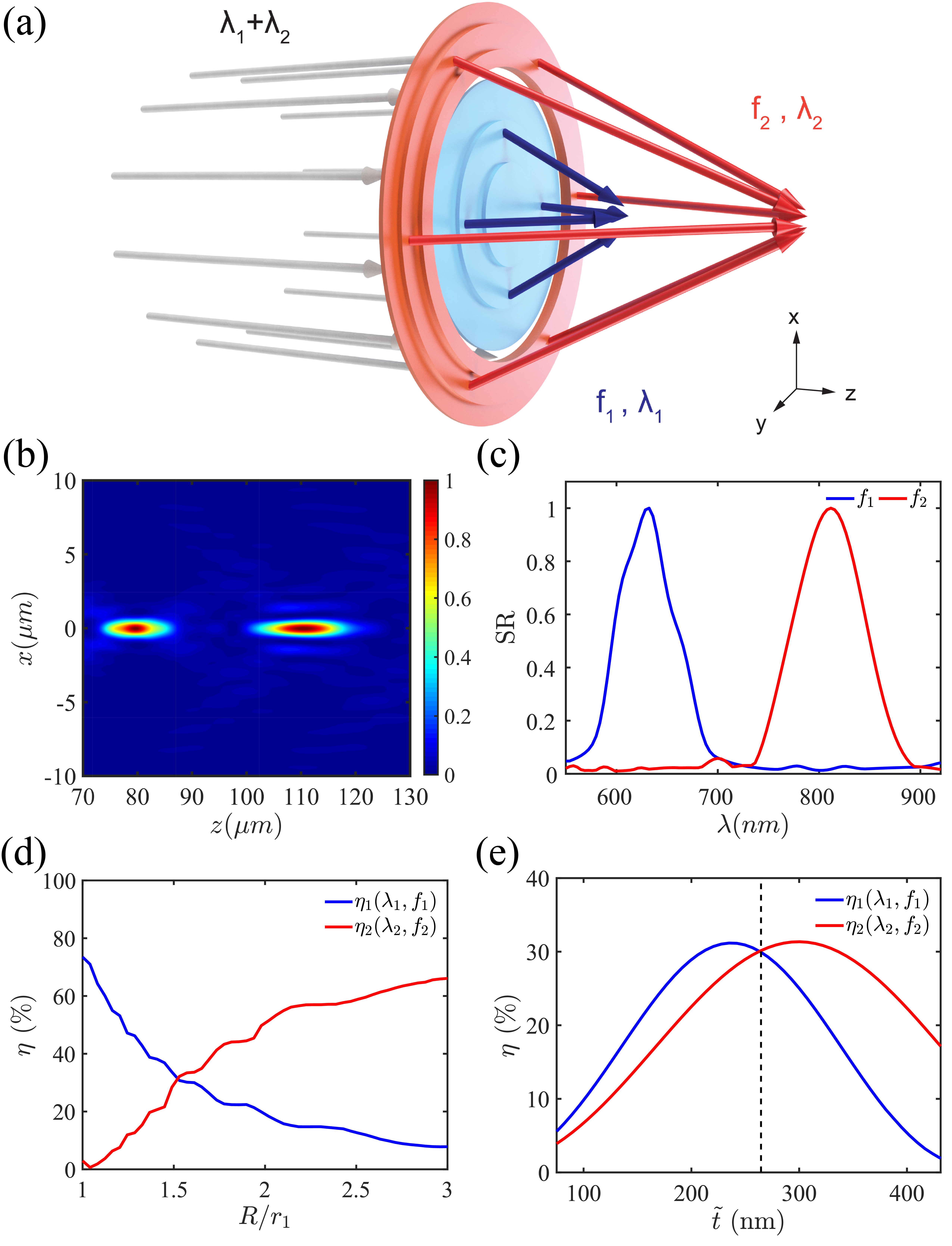
Figure 1(a) illustrates the basic concept of dual-band multi-focal compact diffractive lens elements. These devices are based on two distinct phase modulations spatially separated into an inner circular region, shown in light blue, and an outer annular region, shown in orange, interlocked on the same device plane. Each phase component is responsible for focusing a distinct wavelength band at a selected focal position along the optical -axis. Namely, upon illumination with a polychromatic spectrum this device will focus selected wavelength bands centered around and at pre-defined distances and along the -axis. This operation mechanism differs from traditional multi-focal lenses that generate multiple longitudinal focal spots for the same wavelength Chen et al. (2015); Williams et al. (2017). Rather, our device design enables the simultaneous focusing of different spectral bands either at separate focal points or at the same one.
We study the wave diffraction problem of the proposed dual-band multi-focal MDL using the rigorous Rayleigh-Sommerfeld (RS) first integral formulation. This approach is valid beyond the paraxial approximation Goodman (2017). We consider devices located on the plane illuminated by a normally incident plane wave, which results in a diffracted field that propagates along the direction. The field amplitude is computed according to RS with the following expressions:
| (1) | |||
| (2) |
Here denotes the convolution operation, while and are the complex transverse field distributions of the object and of the image, respectively. Furthermore, is the incident wavenumber, and , where is the distance between the device and image plane. We consider , where is the phase profile on the device that is explicitly represented as:
| (3) |
where and indicate the maximum radial extensions of the first and of the second phase components, respectively. We utilize the phase profiles of separate Fresnel lenses because they guarantee large focusing efficiency around each of the operating wavelengths of the two targeted spectral bands and at the focal lengths . The subscripts in eq. (3) indicate the reduction by modulo . This phase design retains rotational symmetry along the optical axis, which preserves polarization independence. Likewise, it ensures a rotationally symmetric point spread function (PSF) for improved focusing and imaging quality. In the present study, we have discretized the phase profile into four levels, which significantly improves ease of fabrication by requiring only two different lithographic steps.
As a proof of principle, we have selected visible and near-infrared (NIR) spectral regions centered at nm and nm. In addition, we have chosen the small focal distances m and m, which are compatible with on-chip multi-layer detector technologies Tang et al. (2019); Gunapala et al. (2010). We remark that by changing the radial extension of the first and second phase components, we can control both their relative intensity and focusing efficiency. Indeed, by choosing , we can design a device with equal focusing intensities at two well-separated focal lengths. This is shown in panel (b) where we report the intensity distribution profile of the two focal spots on the -plane. Furthermore, its spectral response (SR), defined as the maximum field intensity at the two designed focusing planes (m and m) as a function of wavelengths, is shown in Fig. 1 (c). Our results demonstrate that the two wavelength bands are not only well-separated spatially, but also spectrally. This feature is important in multispectral imaging applications Tang et al. (2019); Gunapala et al. (2010) and for the integration with optoelectronic devices Arbabi et al. (2015). Moreover, we can also independently control the focusing efficiencies and of the inner and outer phase components through the geometrical ratio . This is demonstrated in Fig. 1 (d). In our work, we define the focusing efficiency as the ratio of the image plane intensity within a spot size of three times the full-width-at-half-maximum (FWHM) to the incident intensity profile integrated over the entire device area Banerji et al. (2019); Arbabi et al. (2015):
| (4) |
From Fig. 1 (d), evaluated considering , we find that a value of equalizes the two efficiencies such that . Note that, in addition to retaining the previously defined parameter values, we have also set m (see Supplement 1 for more details regarding the dependance of the device performance on ). We selected m and m to fabricate and experimentally characterize the designed compact microlens.
We recall that MDLs exploit variations in the thickness of materials to impart desired phase delays on the incident radiation. In order to satisfy the designed phase condition of our dual-band device, the material thickness of the inner region and outer annular region have to be equal to , where is refractive index and . Therefore, four lithography process steps are required to fabricate the resulting device. However, to ease this fabrication process, we can identify a central wavelength to determine an effective total device thickness = across the entire device area, reducing the required lithographic process steps to only two with a small reduction in the overall efficiency. This is reported in Fig. 1 (e) where we display the focusing efficiency of the inner ( in blue line) and outer ( in red line) phase components as a function of . Specifically, an effective device thickness equal to 266 nm, indicated by the black dashed line in Fig. 1 (e), equalizes and to 30%, resulting in a reduction of only 1 with respect to the results of panel (d).
III Growth and fabrication method
Reactively sputtered hydrogenated amorphous Si (a-Si:H) enables the compact realization of our design. This material has excellent transparency and a high refractive index () at visible and NIR wavelengths. Likewise, physical deposition by sputtering is a low cost and scalable process. Markedly, well-hydrogenated and alloyed low-loss a-Si:H is transparent until a sharp increase in the optical absorption edge between 2.1 and 2.2 , representing an optical bandgap Moustakas (1979). However, sputtered a-Si:H dispersion and optical properties are highly dependent on deposition conditions. The a-Si:H thin films in this study were grown reactively on fused silica, SiO2, substrates using a Denton Discovery D8 magnetron sputtering system. In preparation before deposition, substrates were solvent washed, sonicated, and plasma ashed in an O2 atmosphere (M4L, PVA TePla America). The a-Si:H films were deposited using the following conditions: sputtering base pressure was kept below Torr, deposition pressure was kept at mTorr with a Ar:H2 gas flow ratio of 4:1 Sccm, substrate was heated to C, and RF deposition power on the intrinsic Si target was set to 200W. The materials’ optical dispersion was characterized using ellipsometry (V-VASE, J.A. Woollam) on 50 nm films. Our deposition process was optimized so that the final films used for fabrication have an average index of and absorption coefficient of cm-1 across the entire operational range. Detailed film characterization is provided in the Supplement 1.
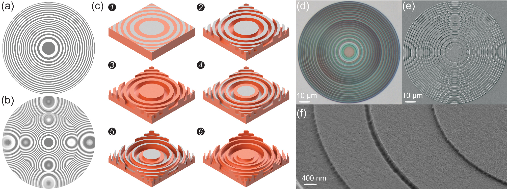
As discussed in the previous section, we identify an effective total device thickness . As a consequence, our fabrication method uses only two lithography process steps to realize a four-level discretized device. Figure 2 (a-b) show the first and second etch mask designs, respectively. The first etch mask is created by combining the and level phase areas, and the second etch mask is the combination of the and level areas. The general fabrication process flow is shown in Fig. 2 (c). Steps 1 through 3 and 4 through 6 are associated with the first and second process iterations, respectively. First, steps 1 and 4 are the lithographic patterning of the first and second etch mask, respectively. The designed etch masks are transferred to metal hard masks with lithography and electron beam evaporation using a positive resist and a lift-off process. Next, steps 2 and 5 are deep anisotropic etches of thicknesses with target values nm and nm, respectively. Finally, steps 3 and 6 are wet etch removals of the residual hard masks.
Our specific fabrication process utilizes electron beam lithography (EBL), a Cr hardmask, and a reactive ion etching (RIE) anisotropic dry etch for both processing iterations. In addition, we deposit Au alignment marks with Ti adhesion layers before device fabrication. For the lithography process, MicroChem PMMA A3 positive resist was spun at 3000 rpm and baked in an oven at 170 for 20 min. After both resist baking steps, a thin conducting layer of Au was deposited using a Cressington 108 Manual Sputter Coater. Details on the exposure and etching processes of our device are reported in the Supplement 1.
Figure 2 (d-e) show optical and SEM images of the top view of the fabricated device. Each of the four phase layers in Fig. 2 (d) are distinguishable as different colors because of color enhancement by optical interference effects. The phase jump at is clear in both of these images. A higher magnification angled SEM image of the fabricated device is shown in Fig.2 (f). This image shows all four levels of the fabricated device. However, due to the etch rate reduction associated to the RIE lag, the total device thickness of the fabricated device results to be 235 nm Jansen et al. (1997) (see also Supplement 1 for more details).
IV Optical characterization method
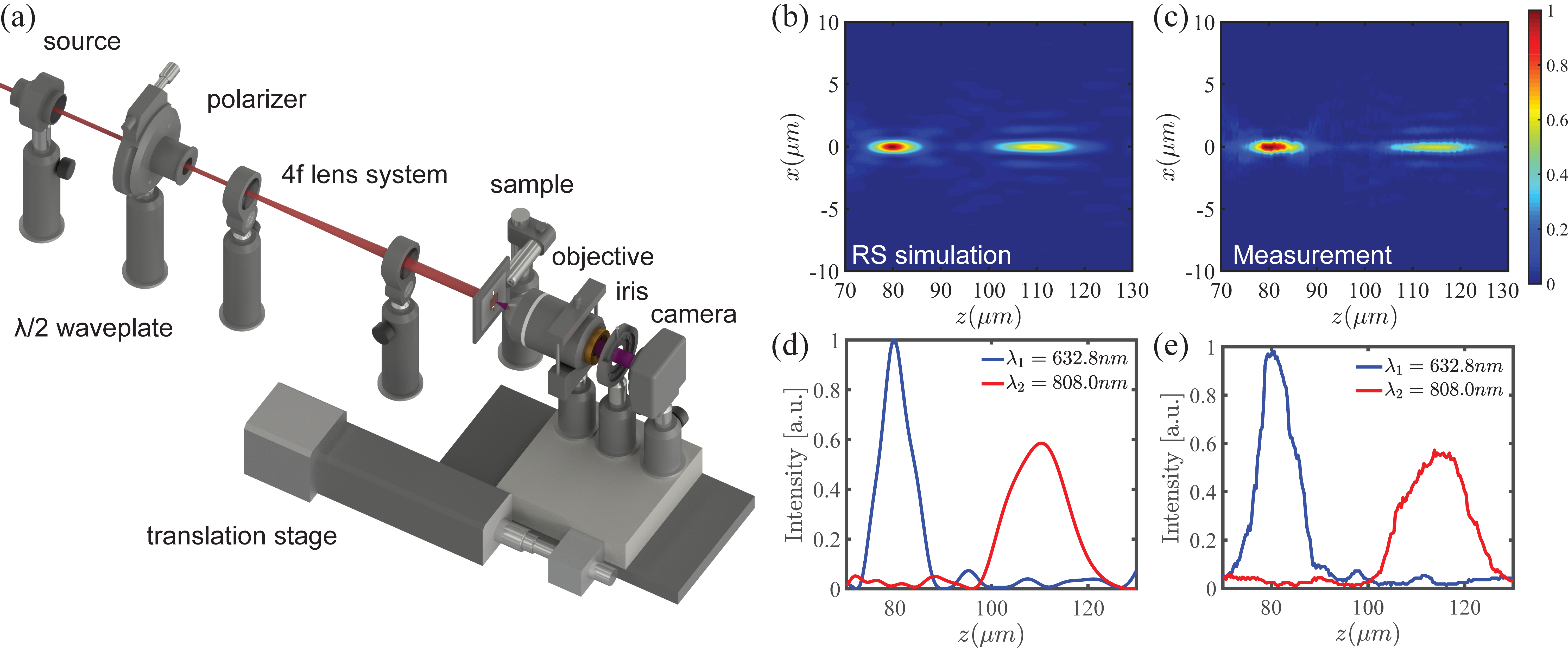
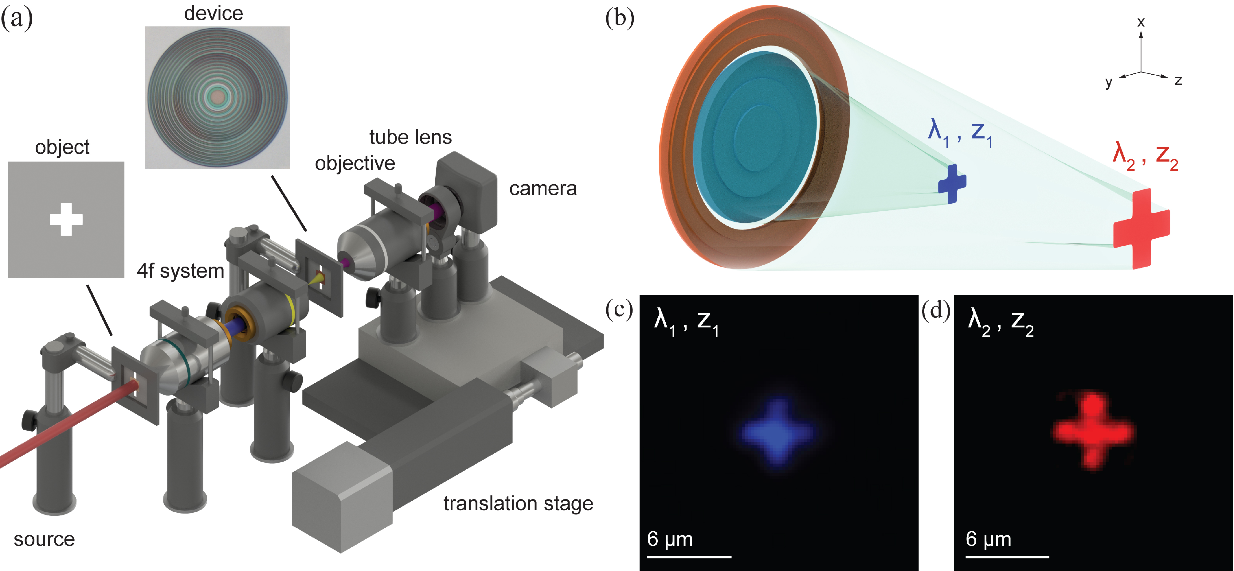
The performances of the fabricated devices are experimentally characterized using the customized visible and near-infrared (NIR) imaging system with -translation capabilities, as illustrated in Fig.3 (a). It utilizes a tunable Ti:sapphire (Mai Tai, Spectra-Physicsop) quasi-CW laser source ( pulse width, but with MHz repetition rate) that allows wavelength selective measurements over a broad visible and NIR spectral band (690 nm – 1000 nm), and a HeNe laser (Hughes 3225H-PC) for characterization at 632.8 nm. We incorporate a waveplate and a linear polarizer to attenuate both sources. In addition, a lens system is used to expand the beam, which approximates a plane wave source illumination and reduces any contribution from beam convergence or divergence. An imaging system consisting of a 0.9 numerical aperture (NA) objective (Olympus MPLFLN100xBDP), an iris (to remove stray reflections), and a CMOS camera (Thorlabs DCC1645C, with short-pass filter removed) is translated along the -axis in unison by a motorized translation stage (Thorlabs LNR50S). This allows the characterization of the image plane intensity profile as a function of distance along the -axis.
The - and -axis scaling was calibrated using an Au alignment mark with known dimensions. The reference data was measured by a transverse translation away from the device and imaging the bare substrate and residual a-Si:H film. Reference and signal data were taken at different exposure times to compensate for the increase in intensity due to focusing. The dark background average was subtracted from both data sets to compensate for the different exposure times.
V Results and discussion
Our dual-band multi-focal compact microlens was initially characterized at its operation wavelengths, = 632.8 nm and = 808 nm. Figure 3 (b) shows the expected electric field intensity distribution in the -plane, normalized with respect to its maximum. This plot shows that the two targeted wavelengths are both well focused at their designed focal distances m (thus a NA of 0.4) and m (thus a NA of 0.47), respectively. Figure 3 (c) displays the measured intensity distribution in the -plane, also normalized with respect to its maximum. This analysis was performed by combining a series of images taken parallel to the device plane when scanning the -axis with a resolution of 0.3 m. The measurements are in excellent agreement with the simulations demonstrating the validity of the proposed approach. In order to compare the position of the maximum value of the focusing intensity along the optical axis as well as the focal depth obtained in the experiments with respect to simulation, we report their intensity cut-profile along the -axis in Figs. 3 (d) and (e), respectively. The measured FWHM of the focal depths of the two phase components, shown in Fig. 3 (e), are found to be equal to and , respectively. These values are close to the predicted ones calculated to be and , respectively (see Fig. 3 (d)). On the other hand, we measured an efficiency of and rather than . This difference in efficiency is due to the small discrepancy in the thickness of the fabricated device with respect to the designed , which is caused by the etch rate variations at small feature sizes Jansen et al. (1997). Specifically, the total thickness of the fabricated device deviates by approximately 30 nm from the designed value of 266 nm that equalizes and . Given the thickness of the fabricated device we can estimate, based on the RS calculations reported in Fig. 1 (e), that the two focusing efficiencies will be different, i.e. and . However, RS simulations, while enabling the analysis of large-scale devices, are based on scalar diffraction theory. Therefore, these simulations do not account for vector coupling effects that become important when the incident radiation interacts with the features of the device that are comparable in size or smaller than the wavelength, resulting in a wavelength-dependent efficiency drop. Often referred to as ”light shadowing effects”, these vector diffraction effects include reflection losses and the resonant behavior observed in devices with high numerical apertures Lalanne et al. (1999); Golub and Friesem (2007). See Supplement 1 for more details regarding full-vector simulations using the Finite Element Method (FEM).
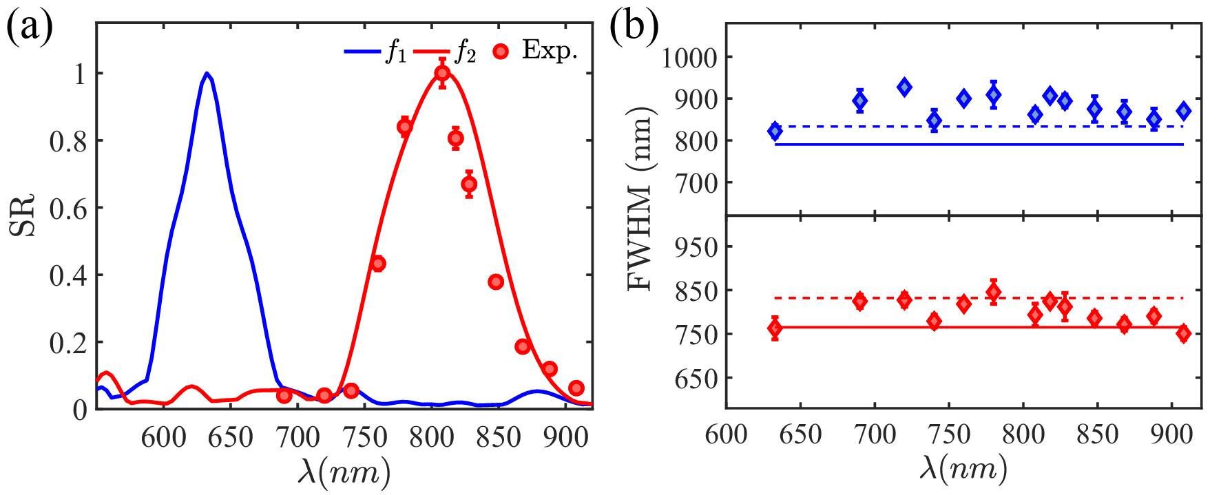
In order to further characterize the dual-band mechanism, we display in Fig. 4 (a) both the normalized measured and simulated spectral response.The experimental SR at is not shown since most of its spectral bandwidth lies outside our laser source wavelength range. On the other hand, we have verified that the spectral bandwidth of the second focus at is consistent between experiment and measurement. Indeed, the simulated and measured FWHM of these spectral responses are equal to 120 nm and 100 nm, respectively.
Moreover, we characterized the FWHM of the two focal spots in Fig. 4 (b). This parameter quantifies the ability of our device to concentrate electromagnetic radiation. Specifically, the diffraction-limit of a annular focusing system is described by Rivolta (1986):
| (5) |
where , , and is the first order Bessel function of the first kind. This function results in an intensity distribution similar to an Airy pattern but with slightly increased intensity in the side lobes. Indeed, eq. 5 reproduces a standard Airy pattern when and substituting , , and with , , and in . By solving eq.(5) at different focal planes for different incident wavelengths as a function of when =0.5, we obtain the analytical FWHM spectrum of the point spread functions of the inner and outer phase component. We compare these analytical results in Fig. 4 (b) with respect to the simulated (dashed lines) and the measured (markers) FWHM as a function of . The experimental results were found to be in good agreement with the simulated values with only a slightly larger FWHM than theory in both cases. These data demonstrate that dual-band multi-focal diffractive lenses produce almost diffraction-limited focal spots at different operation wavelengths.
VI Imaging behavior
There is a growing interest in the engineering of flat optical components with the ability to form well-separated images at different positions along both the longitudinal Chen et al. (2015); Williams et al. (2017) and vertical directions Khorasaninejad et al. (2016b). In these devices the positions of the focal points are controlled with the helicity or with the polarization of the incident light. In this section, we demonstrate that the developed multi-focal diffractive lenses provide wavelength-controlled multi-focal imaging using unpolarized light illumination. This results in the formation of two independent images at two different positions depending on the wavelength, as demonstrated in Fig. 5. In Fig. 5(a) we display a schematic picture of the optical setup used to characterize the dual-band imaging performance of our device. Here, we image our object positioned before the compact dual-band multi-focal MDL using a 4f imaging system consisting of two objectives. The imaging behavior of the MDL as a function of position along the -axis can then be characterized by an imaging setup consisting of a high NA objective, tube lens, and camera all mounted on a motorized translation stage. In our experiment we image a 60 m long cross-shaped object defined in a 300 m by 300 m wide square region obtained using a lift-off process with a 50 nm thick Cr mask on SiO2. We illuminate our object at and using a halogen lamp filtered by a monochromator (Cornerstone 260) and collimated. The operation principle of the fabricated dual-band multi-focal device is illustrated in Fig. 5 (b). Considering the geometry of our experimental setup, the images will be formed at the plane positions and , as predicted by using the Gaussian lens equation Goodman (2017):
| (6) |
where equal to 350m is the object distance. As predicted by eq. (6), Fig. 5(c-d) show two clear images of our object at =102 m and =155 m when illuminating with and , respectively. These results demonstrate that two images are formed for the two selected narrow bands at designed locations along the longitudinal direction.
VII Conclusion
In conclusion, we have designed, fabricated, and characterized compact visible and NIR dual-band multi-focal diffractive microlenses. These devices are based on high-index materials compatible with very large scale integration fabrication methodologies resulting in a considerable reduction in cost, complexity, and size compared to alternative implementations based on the meta-lens approach. The proposed multifunctional microlens design shows the capability to focus two different incident wavelengths at two different focal positions along the optical axis. Moreover, the same design concept demonstrated here can be applied to simultaneously focus predefined spectral bands at the same focal spot. This allows integration atop advanced on-chip detector architectures, enabling ultra-compact multispectral devices for imaging and spectroscopic on-chip applications Tang et al. (2019). For instance, our devices could be used as multispectral microlens arrays for differential multiphoton microscopy Hoover et al. (2011); Bewersdorf et al. (1998); Beaulieu et al. (2020). Finally, we have shown that dual-band multi-focal microlenses can image, under unpolarized illumination, an object at two designed focal positions depending on the incident wavelength. This enables the encoding of the depth information of a sample into different spectral images, i.e. multispectral confocality Tearney et al. (2002), which can be exploited for 3D image reconstruction and in future tomographic applications.
Funding Information
Army Research Laboratory (ARL) (Cooperative Agreement Number W911NF-12-2-0023); National Science Foundation (NSF) (DMR 1709704).
Acknowledgements
L.D.N. would like to thank Prof. Enrico Bellotti for insightful discussions on the presented technology.
Disclosures
The authors declare no conflicts of interest.
See Supplement 1 for supporting content.
VIII Supplementary Information
This will usually read something like: “Experimental procedures and characterization data for all new compounds. The class will automatically add a sentence pointing to the information on-line:
References
- Lu and Fei (2014) Guolan Lu and Baowei Fei, “Medical hyperspectral imaging: a review,” Journal of biomedical optics 19, 010901 (2014).
- Kasischke et al. (1997) Eric S Kasischke, John M Melack, and M Craig Dobson, “The use of imaging radars for ecological applications review,” Remote sensing of environment 59, 141–156 (1997).
- Shimoni et al. (2019) Michal Shimoni, Rob Haelterman, and Christiaan Perneel, “Hypersectral imaging for military and security applications: Combining myriad processing and sensing techniques,” IEEE Geoscience and Remote Sensing Magazine 7, 101–117 (2019).
- Herzig (2014) Hans Peter Herzig, Micro-optics: elements, systems and applications (CRC Press, 2014).
- Kress and Meyrueis (2009) Bernard C Kress and Patrick Meyrueis, Applied Digital Optics: from micro-optics to nanophotonics (John Wiley & Sons, 2009).
- Capasso (2018) Federico Capasso, “The future and promise of flat optics: a personal perspective,” Nanophotonics 7, 953–957 (2018).
- Genevet et al. (2017) Patrice Genevet, Federico Capasso, Francesco Aieta, Mohammadreza Khorasaninejad, and Robert Devlin, “Recent advances in planar optics: from plasmonic to dielectric metasurfaces,” Optica 4, 139–152 (2017).
- Banerji et al. (2019) Sourangsu Banerji, Monjurul Meem, Apratim Majumder, Fernando Guevara Vasquez, Berardi Sensale-Rodriguez, and Rajesh Menon, “Imaging with flat optics: metalenses or diffractive lenses?” Optica 6, 805–810 (2019).
- Hu et al. (2016) Xin Hu, Gaiqi Xu, Long Wen, Huacun Wang, Yuncheng Zhao, Yaxin Zhang, David RS Cumming, and Qin Chen, “Metamaterial absorber integrated microfluidic terahertz sensors,” Laser & Photonics Reviews 10, 962–969 (2016).
- Cheben et al. (2018) Pavel Cheben, Robert Halir, Jens H Schmid, Harry A Atwater, and David R Smith, “Subwavelength integrated photonics,” Nature 560, 565–572 (2018).
- Romagnoli et al. (2018) Marco Romagnoli, Vito Sorianello, Michele Midrio, Frank HL Koppens, Cedric Huyghebaert, Daniel Neumaier, Paola Galli, Wolfgang Templ, Antonio D’Errico, and Andrea C Ferrari, “Graphene-based integrated photonics for next-generation datacom and telecom,” Nature Reviews Materials 3, 392–414 (2018).
- Redding et al. (2013) Brandon Redding, Seng Fatt Liew, Raktim Sarma, and Hui Cao, “Compact spectrometer based on a disordered photonic chip,” Nature Photonics 7, 746 (2013).
- Boschetti et al. (2019) Alice Boschetti, Andrea Taschin, Paolo Bartolini, Anjani Kumar Tiwari, Lorenzo Pattelli, Renato Torre, and Diederik S Wiersma, “Spectral super-resolution spectroscopy using a random laser,” Nature Photonics , 1–6 (2019).
- Kildishev et al. (2013) Alexander V Kildishev, Alexandra Boltasseva, and Vladimir M Shalaev, “Planar photonics with metasurfaces,” Science 339, 1232009 (2013).
- Koenderink et al. (2015) A Femius Koenderink, Andrea Alu, and Albert Polman, “Nanophotonics: shrinking light-based technology,” Science 348, 516–521 (2015).
- Zheludev and Kivshar (2012) Nikolay I Zheludev and Yuri S Kivshar, “From metamaterials to metadevices,” Nature materials 11, 917–924 (2012).
- Yu et al. (2011) Nanfang Yu, Patrice Genevet, Mikhail A Kats, Francesco Aieta, Jean-Philippe Tetienne, Federico Capasso, and Zeno Gaburro, “Light propagation with phase discontinuities: generalized laws of reflection and refraction,” science 334, 333–337 (2011).
- Yu and Capasso (2014) Nanfang Yu and Federico Capasso, “Flat optics with designer metasurfaces,” Nature materials 13, 139–150 (2014).
- Zhang and Liu (2008) Xiang Zhang and Zhaowei Liu, “Superlenses to overcome the diffraction limit,” Nature materials 7, 435–441 (2008).
- Rogers et al. (2012) Edward TF Rogers, Jari Lindberg, Tapashree Roy, Salvatore Savo, John E Chad, Mark R Dennis, and Nikolay I Zheludev, “A super-oscillatory lens optical microscope for subwavelength imaging,” Nature materials 11, 432–435 (2012).
- Lalanne and Chavel (2017) Philippe Lalanne and Pierre Chavel, “Metalenses at visible wavelengths: past, present, perspectives,” Laser & Photonics Reviews 11, 1600295 (2017).
- Zhu et al. (2017) Alexander Y Zhu, Arseniy I Kuznetsov, Boris Luk’yanchuk, Nader Engheta, and Patrice Genevet, “Traditional and emerging materials for optical metasurfaces,” Nanophotonics 6, 452–471 (2017).
- Kuznetsov et al. (2016) Arseniy I Kuznetsov, Andrey E Miroshnichenko, Mark L Brongersma, Yuri S Kivshar, and Boris Luk’yanchuk, “Optically resonant dielectric nanostructures,” Science 354, aag2472 (2016).
- Arbabi et al. (2015) Amir Arbabi, Yu Horie, Alexander J Ball, Mahmood Bagheri, and Andrei Faraon, “Subwavelength-thick lenses with high numerical apertures and large efficiency based on high-contrast transmitarrays,” Nature Communications 6, 7069 (2015).
- Khorasaninejad et al. (2016a) Mohammadreza Khorasaninejad, Alexander Yutong Zhu, Charles Roques-Carmes, Wei Ting Chen, Jaewon Oh, Ishan Mishra, Robert C Devlin, and Federico Capasso, “Polarization-insensitive metalenses at visible wavelengths,” Nano Letters 16, 7229–7234 (2016a).
- Chen et al. (2019) Wei Ting Chen, Alexander Y Zhu, Jared Sisler, Zameer Bharwani, and Federico Capasso, “A broadband achromatic polarization-insensitive metalens consisting of anisotropic nanostructures,” Nature Communications 10, 355 (2019).
- Lin et al. (2014) Dianmin Lin, Pengyu Fan, Erez Hasman, and Mark L Brongersma, “Dielectric gradient metasurface optical elements,” Science 345, 298–302 (2014).
- Zheng et al. (2015) Guoxing Zheng, Holger Mühlenbernd, Mitchell Kenney, Guixin Li, Thomas Zentgraf, and Shuang Zhang, “Metasurface holograms reaching 80% efficiency,” Nature Nanotechnology 10, 308 (2015).
- Zhan et al. (2016) Alan Zhan, Shane Colburn, Rahul Trivedi, Taylor K Fryett, Christopher M Dodson, and Arka Majumdar, “Low-contrast dielectric metasurface optics,” ACS Photonics 3, 209–214 (2016).
- Fleming and Hutley (1997) Madeleine B Fleming and MC Hutley, “Blazed diffractive optics,” Applied optics 36, 4635–4643 (1997).
- Swanson (1989) Gary J Swanson, Binary optics technology: the theory and design of multi-level diffractive optical elements, Tech. Rep. (MASSACHUSETTS INST OF TECH LEXINGTON LINCOLN LAB, 1989).
- Mohammad et al. (2018) Nabil Mohammad, Monjurul Meem, Bing Shen, Peng Wang, and Rajesh Menon, “Broadband imaging with one planar diffractive lens,” Scientific reports 8, 1–6 (2018).
- Chao et al. (2005) David Chao, Amil Patel, Tymon Barwicz, Henry I Smith, and Rajesh Menon, “Immersion zone-plate-array lithography,” Journal of Vacuum Science & Technology B: Microelectronics and Nanometer Structures Processing, Measurement, and Phenomena 23, 2657–2661 (2005).
- Davidson et al. (1991) N Davidson, AA Friesem, and E Hasman, “Holographic axilens: high resolution and long focal depth,” Optics letters 16, 523–525 (1991).
- Tang et al. (2019) Xin Tang, Matthew M Ackerman, Menglu Chen, and Philippe Guyot-Sionnest, “Dual-band infrared imaging using stacked colloidal quantum dot photodiodes,” Nature Photonics 13, 277 (2019).
- Gunapala et al. (2010) S. D. Gunapala, S. V. Bandara, J. K. Liu, J. M. Mumolo, D. Z. Ting, C. J. Hill, J. Nguyen, B. Simolon, J. Woolaway, S. C. Wang, W. Li, P. D. LeVan, and M. Z. Tidrow, “Demonstration of megapixel dual-band qwip focal plane array,” IEEE Journal of Quantum Electronics 46, 285–293 (2010).
- Lutz et al. (2018) H Lutz, R Breiter, D Eich, H Figgemeier, S Hanna, R Oelmaier, and J Wendler, “Towards ultra-small pixel pitch cooled mw and lw ir-modules,” in Infrared Technology and Applications XLIV, Vol. 10624 (International Society for Optics and Photonics, 2018) p. 106240B.
- Gunapala et al. (2010) Sarath D Gunapala, Sumith V Bandara, John K Liu, Jason M Mumolo, David Z Ting, Cory J Hill, Jean Nguyen, Brian Simolon, James Woolaway, Samuel C Wang, et al., “Demonstration of megapixel dual-band qwip focal plane array,” IEEE Journal of Quantum Electronics 46, 285–293 (2010).
- Davies et al. (1994) Neil A Davies, Malcolm McCormick, and Michael Brewin, “Design and analysis of an image transfer system using microlens arrays,” Optical Engineering 33, 3624–3634 (1994).
- Nussbaum et al. (1997) Ph Nussbaum, Reinhard Voelkel, Hans Peter Herzig, Martin Eisner, and Stefan Haselbeck, “Design, fabrication and testing of microlens arrays for sensors and microsystems,” Pure and applied optics: Journal of the European optical society part A 6, 617 (1997).
- Chen et al. (2015) Xianzhong Chen, Ming Chen, Muhammad Qasim Mehmood, Dandan Wen, Fuyong Yue, Cheng-Wei Qiu, and Shuang Zhang, “Longitudinal multifoci metalens for circularly polarized light,” Advanced Optical Materials 3, 1201–1206 (2015).
- Williams et al. (2017) Calum Williams, Yunuen Montelongo, and Timothy D Wilkinson, “Plasmonic metalens for narrowband dual-focus imaging,” Advanced Optical Materials 5, 1700811 (2017).
- Goodman (2017) Joseph W. Goodman, Introduction to Fourier Optics (W. H. Freeman, 2017).
- Moustakas (1979) TD Moustakas, “Sputtered hydrogenated amorphous silicon,” Journal of Electronic Materials 8, 391–435 (1979).
- Jansen et al. (1997) Henri Jansen, Meint de Boer, Remco Wiegerink, Niels Tas, Edwin Smulders, Christina Neagu, and Miko Elwenspoek, “Bsm 7: Rie lag in high aspect ratio trench etching of silicon,” Microelectronic Engineering 35, 45–50 (1997).
- Lalanne et al. (1999) Philippe Lalanne, Simion Astilean, Pierre Chavel, Edmond Cambril, and Huguette Launois, “Design and fabrication of blazed binary diffractive elements with sampling periods smaller than the structural cutoff,” JOSA A 16, 1143–1156 (1999).
- Golub and Friesem (2007) Michael A Golub and Asher A Friesem, “Analytic design and solutions for resonance domain diffractive optical elements,” JOSA A 24, 687–695 (2007).
- Rivolta (1986) Claudio Rivolta, “Airy disk diffraction pattern: comparison of some values of f/no. and obscuration ratio,” Applied optics 25, 2404–2408 (1986).
- Khorasaninejad et al. (2016b) M Khorasaninejad, WT Chen, AY Zhu, J Oh, RC Devlin, D Rousso, and F Capasso, “Multispectral chiral imaging with a metalens,” Nano letters 16, 4595–4600 (2016b).
- Hoover et al. (2011) Erich E Hoover, Michael D Young, Eric V Chandler, Anding Luo, Jeffrey J Field, Kraig E Sheetz, Anne W Sylvester, and Jeff A Squier, “Remote focusing for programmable multi-layer differential multiphoton microscopy,” Biomedical optics express 2, 113–122 (2011).
- Bewersdorf et al. (1998) Jörg Bewersdorf, Rainer Pick, and Stefan W Hell, “Multifocal multiphoton microscopy,” Optics letters 23, 655–657 (1998).
- Beaulieu et al. (2020) Devin R Beaulieu, Ian G Davison, Kıvılcım Kılıç, Thomas G Bifano, and Jerome Mertz, “Simultaneous multiplane imaging with reverberation two-photon microscopy,” Nature Methods 17, 283–286 (2020).
- Tearney et al. (2002) Guillermo J Tearney, Brett E Bouma, and Robert H Webb, “Confocal microscopy with multi-spectral encoding,” (2002), uS Patent 6,341,036.