Harnessing exciton-exciton annihilation in two-dimensional semiconductors
Abstract
Strong many-body interactions in two-dimensional (2D) semiconductors give rise to efficient exciton–exciton annihilation (EEA). This process is expected to result in the generation of unbound high energy carriers. Here, we report an unconventional photoresponse of van der Waals heterostructure devices resulting from efficient EEA. Our heterostructures, which consist of monolayer transition metal dichalcogenide (TMD), hexagonal boron nitride (hBN), and few-layer graphene, exhibit photocurrent when photoexcited carriers possess sufficient energy to overcome the high energy barrier of hBN. Interestingly, we find that the device exhibits moderate photocurrent quantum efficiency even when the semiconducting TMD layer is excited at its ground exciton resonance despite the high exciton binding energy and large transport barrier. Using ab initio calculations, we show that EEA yields highly energetic electrons and holes with unevenly distributed energies depending on the scattering condition. Our findings highlight the dominant role of EEA in determining the photoresponse of 2D semiconductor optoelectronic devices.
Many-body effects manifest themselves as unique photoresponse in nanoscale materials Mak and Shan (2016). Exciton–exciton annihilation (EEA), a four-body interaction involving the energy and momentum transfer between two holes and two electrons, is known to be highly efficient in nanostructures with reduced dimensions, such as quantum dots Gao et al. (2013); Wei et al. (2016), graphene nanoribbons Soavi et al. (2016), carbon nanotubes Ma et al. (2005); Wang et al. (2010), and polymer chains Engel et al. (2006); Nguyen et al. (2000). Recent studies Sun et al. (2014); Mouri et al. (2014); Kumar et al. (2014) indicate that the EEA rate in two-dimensional (2D) Group VI transition metal dichalcogenide (TMD) semiconductors is substantially enhanced even when compared to their bilayer and trilayer samples Yuan and Huang (2015). While the EEA in 2D semiconductors leads to undesirable efficiency droop in photoluminescence (PL) Amani et al. (2015) and electroluminescence (EL) Wang et al. (2017), energy conservation requires hot electron-hole pairs to be generated upon annihilation of individual excitons. Recent study showed that the EEA-generated hot carriers can be harnessed for remarkably efficient optical upconversion in 2D TMD semiconductors Han et al. (2018); Manca et al. (2017), and their heterostructures Binder et al. (2019), inspiring prospects for harnessing highly efficient EEA process in 2D materials to generate hot carriers for energy harvesting application.
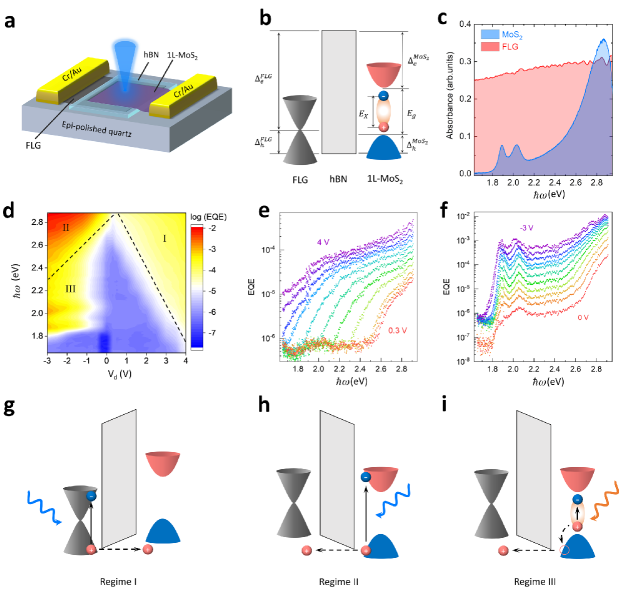
Herein, we report photoresponse originating from EEA-generated hot carriers in a metal-insulator-semiconductor (MIS)-type van der Waals heterostructure device. In this study, “hot” carrier refers to non-thermalized high energy carriers generated by EEA in contrast to thermalized hot carriers in graphene-based photothermoelectric devices Gabor et al. (2011); Song et al. (2011); Sun et al. (2012). The MIS-type heterostructure consists of few-layer graphene (FLG), hexagonal boron nitride (hBN), and monolayer molybdenum disulfide (MoS2) (Figure 1a). The bright optical microscope and atomic force microscope (AFM) image of one of the MIS devices is displayed in the Supporting Information Figure S1. Figure 1b depicts the schematic band diagram of the heterostructure. Because of the low electron affinity and wide band gap of hBN (Figure 1b), it acts as an insulating barrier which blocks charge transfer between the FLG and the MoS2 layer. However, the band alignment between hBN with FLG and MoS2 reveals significantly lower energy barrier for interlayer hole transfer compared to electron transfer Vu et al. (2017); Britnell et al. (2012); Ma et al. (2016); Choi et al. (2013); Jeong et al. (2016). Hence, hBN acts as a carrier- and energy-selective tunnel barrier that selectively favors hot hole transfer. Under forward bias above a specific threshold voltage (), the device exhibits EL at low threshold current densities, evidencing hole tunneling from FLG to MoS2. The tunnel barrier for holes in reverse bias () is similarly low, however, the device remains highly insulating due to the absence of holes in MoS2. The charge transport and EL behavior of the tunnel diode are discussed in Supporting Information S3 and in a previous study Wang et al. (2017).
We investigate the photocarrier dynamics of the heterostructure by measuring the bias-dependent spectral features in the photocurrent generated by photons of varying energy ranging from 1.65 to 2.91 eV. All photocurrent measurements were performed with lock-in technique (Supporting Information S1) Furchi et al. (2014) at room temperature and in vacuum ( mbar). On the basis of the band alignment of the heterostructure, non-negligible photocurrent is only expected when the photoexcited carriers gain sufficient energy to overcome the potential barrier due to hBN (Figure 1b). Note that the FLG exhibits relatively uniform absorption across the visible frequencies whereas monolayer MoS2 absorption exhibits prominent excitonic resonances with three excitonic peaks (Figure 1c). Two types of excitons, A and B, at 1.89 eV and 2.03 eV arise from spin–orbit split bands. Figure 1d shows the external quantum efficiency (EQE), the incident photon to converted electron ratio, as a function of the excitation energy and bias . The EQE value is calculated from the measured photocurrent () as EQE=, where is the optical power, and is the elementary charge.
The spectral features are distinctly different in the forward (Figure 1e) and reverse (Figure 1f) bias regimes, but the common trend is the presence of distinct threshold behaviour. In forward bias, the photocurrent remains negligible at low photon energy before increasing exponentially above the threshold photon energy . The , in turn, decreases linearly with increasing , as shown by the dashed line in Figure 1d. The photocurrent spectrum is featureless above the threshold with no traces of excitonic absorption, suggesting that photocarriers generated in FLG play a dominant role in photocurrent generation (regime I). The maximum is eV at low bias. Here, coincides with the difference between the neutrality point of FLG and the valence-band maximum of hBN, corresponding to the energy barrier for interlayer hole transfer from FLG to MoS2 based on previous studies on photocarrier transport across graphene/hBN interface Britnell et al. (2012); Ma et al. (2016) (Figure 1b). This indicates that the interlayer charge transport of non-thermalized photo-carriers, possibly by Fowler–Nordheim tunnelling or over-barrier direct transport, is responsible for the observed photocurrent above (Figure 1g). Under reverse bias, EQE exhibits a similar threshold behaviour but with two prominent peaks corresponding to A and B excitonic absorption resonances. At the first sight, the threshold behavior can be explained as the onset of hot hole direct tunneling from MoS2 to FLG (see Figure 1h, regime II), similar to the forward bias case albeit in opposite direction. On the other hand, the relatively strong photocurrent in the low-energy excitation regime is unexpected due to high binding energy of excitons and their insufficient kinetic energy to overcome the potential barrier of hBN. Remarkably, the EQE at the exciton resonance in this regime III is comparable to those in regime II, specially under strong reverse bias. The observation of a finite photocurrent at the excitation energy below the quasiparticle bandgap of MoS2 indicates exciton dissociation generating hot holes with sufficient excess energy to overcome potential barrier due to hBN (see Figure 1i).
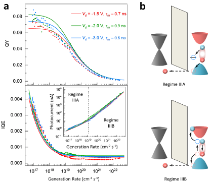
There are two possible mechanisms for hot holes generation through exciton dissociation: disorder-assisted exciton decay and EEA Moody et al. (2016). The exciton dissociation rate through the first mechanism varies linearly with exciton density Wang et al. (2015) while the latter varies quadratically Yu et al. (2016). To distinguish these two mechanisms, we measured photoluminescence (PL) and the photocurrent as a function of excitation power at the excitation energy near the ground-state exciton resonance, well below the quasiparticle band gap of MoS2 and energy required for hole tunnelling from monolayer MoS2 to FLG (Figure 1d,f). This allows us to determine whether the same rate constants consistently describe the behavior of these interdependent phenomena. Figure 2a shows the power dependence of the PL quantum yield (QY) and photocurrent internal quantum efficiency (IQE) measured concurrently on the same sample with 633 nm (1.96 eV) laser as the excitation source. The experimental details and the calculation of PL QY and IQE are described in Supporting Information S1.
The PL QY is nearly constant at low photocarrier generation rates and gradually decreases with increasing radiation power. In contrast, the photocurrent IQE drops initially and saturates to a finite value in the high-power regime. The steady-state exciton concentration can be found by balancing the electron-hole generation rate with the total exciton decay rate as
| (1) |
where is the EEA rate, is the reciprocal exciton lifetime with and being the radiative and non-radiative exciton relaxation times, respectively. The latter is mostly due to charge traps Wang et al. (2015) with an additional contribution from electron-exciton annihilation Lien et al. (2019), which is particularly relevant for n-doped samples. The charge traps are expected to be sulfur vacancies, which are the most energetically favorable type of defect Santosh et al. (2014). By tuning the Fermi level through an external electric field, we change the equilibrium occupation of traps altering their charge trapping efficiency. Thus, the electron-exciton annihilation rate also changes with bias Lien et al. (2019). Hence, differs for each PL QY curve shown in Figure 2a. The theoretical QY is given by the ratio between radiative recombination and generation rates, , where is the solution of equation (1). In the low-power (or linear-response) limit, the QY approaches a constant given by the ratio that at the same time determines the maximum QY for a given voltage. In the high-power limit the QY decreases with increasing as because EEA reduces the steady-state concentration of excitons. The kinetic model in equation 1 describes the power-dependence of QY observed in experimental data with fitting parameters of cm2/s, ns and to ns. The fitting parameters are consistent with earlier studies in monolayer MoS2 Sun et al. (2014); Yu et al. (2016) and other 2D semiconductors such as MoSe2Kumar et al. (2014), WS2 Yuan and Huang (2015), and WSe2Mouri et al. (2014).
While EEA leads to reduction of exciton population and therefore diminishes the PL QY, it generates hot carriers that can overcome the hBN barrier and contribute to photocurrent. For the IQE model, we consider the concentration of such hot holes denoted by . Here, EEA competes with high-energy carrier-carrier collisions leading in particular to impact ionization, which is described by the rate of the order of cm2/s. The same process makes the high-energy holes thermalize by collisions with lower energy carriers, hence, lose the energy required to escape the semiconductor. At the typical – cm-2, the corresponding carrier-carrier collision time is of the order of – fs, consistent with literature values in bulk Rota et al. (1993) and 2D semiconductors Grubisic Cabo et al. (2015); Nie et al. (2014). The rate equation for can be written as
| (2) |
where is the interlayer transport time (ns scaled), and the corresponding is given by the ratio between the transport and generation rates. Equation (2) is deduced in Supporting Information S1. In contrast to a recent work Arp et al. (2019), we do not use ultrafast pulses and consider the rate equation in the steady-state limit. The model does not account for the carrier-phonon interactions because photocarrier thermalization is dominated by the carrier-carrier scattering away from the band edges Ciccarino et al. (2018).
The defect-assisted non-radiative recombination is also responsible for the hole generation (as shown in Figure 2b) that connects equations (1) and (2). In the simplest case, when no barrier exists and all the photoexcited carriers can escape the semiconductor, the terms containing and are not relevant, and we obtain . In MIS heterostructure case, the hBN barrier places the hole escape window to rather high energies ( eV or greater with respect to the top of the MoS2 valence band), and the holes rapidly leave the window while thermalizing. Because of carrier-carrier scattering being a quadratic function of carrier concentration, the resulting IQE is strongly diminished with increasing excitation rate. However, EEA compensates the carrier-thermalization process at high excitation densities and prevents the IQE from falling to zero. In the limit of high photocarrier generation rates, we obtain a saturated IQE independent of given by
| (3) |
This model fits the experimentally observed trend, as shown in Figure 2a. The saturation of the IQE at high photocarrier generation rates is a clear manifestation that the photocurrent generation involves EEA.
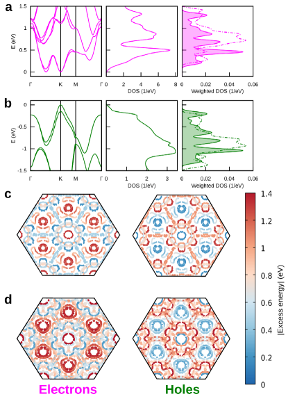
In EEA process, nonradiative exciton recombination ionizes another exciton. Considering energy conservation law, the ionization energy is equal to the energy released during recombination process. This recombination energy is equal to excitation energy and for excitons A and B, respectively. Ionization energy equals the sum of the exciton binding energy and the excess energy shared between the free electron and hole created. The exciton binding energies are given as follows: . Further, the momentum conservation law dictates that the electron and hole wave vectors of ionized exciton must be opposite in direction, although equal in magnitude, in the absence of Umklapp processes. Hence, there is a finite range of possible allowed states in electronic structure of MoS2 that satisfies the energy and momentum restrictions. Here, we identify the allowed transition states within the first Brillouin zone of MoS2 EEA processes to generate hot carriers that can contribute to photocurrent generation using density functional theory (DFT) modeling. The wave vectors are counted with respect to the corner of the Brillouin zone, where the electron-hole pairs emerge due to EEA. Through scissor operators, we manually adjust the quasiparticle bandgap to the experimental value of eV since the theory does not reliably predict quasiparticle energies Martin and Martin (2004). Figure 3a,b shows the band structure, density of states (DOS), and the DOS weighted with the probability to occupy the states due to EEA. Figure 3c,d shows the final wave vectors of electrons and holes in the Brillouin zone with their excess energies encoded in color. Note that the final electron and hole states are asymmetric such that one of the two resulting particles tends to gain more energy than the other. To contribute to photocurrent generation, hot free holes need to overcome the transport barrier due to hBN band gap. The excess energy required is estimated to be 0.4 eV or greater (Figure 1b) Vu et al. (2017). Our DFT modeling demonstrates that holes derived from recombination of both A and B excitons possess sufficient excess kinetic energies ( 1 eV) to contribute to photocurrent (Figure 2b).
In summary, we have shown that EEA in 2D semiconductors can be harnessed in photocarrier transport in vdW heterostructures. EEA rate in 2D semiconductor is significantly enhanced compared to bulk semiconductor to generate clear photoresponse in the excitation power range of ordinary optoelectronic devices, corresponding to photocarrier generation rates greater than cm-2s-1. We note that the observed effect is not limited to monolayer MoS2. We have also observed the equivalent effects in devices based on FLG/hBN/WS2 heterostructure despite higher barrier that the holes must overcome to yield photocurrent (see Supporting Information S5). Although the efficiency of these unoptimized devices is limited, we envision that an intelligent heterostructure design by material selection and band gap engineering will enable improved energy-harvesting devices by exploiting EEA processes in 2D semiconductors.
Contributions
G.E. and E.L. conceived the idea of the work. E.L. fabricated the MIS heterostructure devices and performed electro-optical measurements and other sample characterizations with guidance from I.V. and D.V. I.V. and D.V. devised and assembled the necessary electro-optical setup. D.Y. theoretically explored the EEA generation channels under supervision of F.P. and M.T. K.W. and T.T. provided hBN crystals. M.T. and G.E. managed the project, analyzed the data, devised the model, and wrote the manuscript with inputs from E.L., D.Y. and F.P.
Acknowledgements
G.E. acknowledge the Singapore National Research Foundation (NRF) for funding the research under the Medium Sized Centre Programme R-723-000-001-281. G.E. also acknowledges support from the Ministry of Education (MOE), Singapore, under AcRF Tier 2 (MOE2017T2-1-134) and Tier 3 (MOE2018-T3-1-005). K.W. and T.T. acknowledge support from the Elemental Strategy Initiative conducted by the MEXT, Japan and the CREST (JPMJCR15F3), JST. M.T. acknowledges the Director’s Senior Research Fellowship from the Centre for Advanced 2D Materials at the National University of Singapore (funded jointly through Singapore NRF Medium Sized Centre Programme [R-723-000-001-281] and NUS Young Investigator Award [R-607-000-236-133]). D.Y. and F.P. were funded by the Collaborative Research Center (SFB) 767 of the German Research Foundation (DFG). An important part of the numerical modeling was carried out on the computational resources of the bwHPC program, namely the bwUniCluster and the JUSTUS HPC facility.
Competing Interests
The authors declare no competing interests.
Additional Information
Supporting Information is available free of charge at https://pubs.acs.org/doi/10.1021/acs.nanolett.9b04756
Correspondence and requests for supplemental materials should be addressed to either M.T.
(theory, c2dmt@nus.edu.sg) or G.E. (experiment, g.eda@nus.edu.sg).
References
- Mak and Shan (2016) K. F. Mak and J. Shan, Nature Photonics 10, 216 (2016).
- Gao et al. (2013) Y. Gao, C. S. S. Sandeep, J. M. Schins, A. J. Houtepen, and L. D. A. Siebbeles, Nature Communications 4, 2329 (2013).
- Wei et al. (2016) K. Wei, X. Zheng, X. Cheng, C. Shen, and T. Jiang, Advanced Optical Materials 4, 1993 (2016).
- Soavi et al. (2016) G. Soavi, S. Dal Conte, C. Manzoni, D. Viola, A. Narita, Y. Hu, X. Feng, U. Hohenester, E. Molinari, D. Prezzi, et al., Nature Communications 7, 11010 (2016).
- Ma et al. (2005) Y.-Z. Ma, L. Valkunas, S. L. Dexheimer, S. M. Bachilo, and G. R. Fleming, Phys. Rev. Lett. 94, 157402 (2005).
- Wang et al. (2010) S. Wang, M. Khafizov, X. Tu, M. Zheng, and T. D. Krauss, Nano Letters 10, 2381 (2010).
- Engel et al. (2006) E. Engel, K. Leo, and M. Hoffmann, Chemical Physics 325, 170 (2006).
- Nguyen et al. (2000) T.-Q. Nguyen, I. B. Martini, J. Liu, and B. J. Schwartz, The Journal of Physical Chemistry B 104, 237 (2000).
- Sun et al. (2014) D. Sun, Y. Rao, G. A. Reider, G. Chen, Y. You, L. Brezin, A. R. Harutyunyan, and T. F. Heinz, Nano Letters 14, 5625 (2014).
- Mouri et al. (2014) S. Mouri, Y. Miyauchi, M. Toh, W. Zhao, G. Eda, and K. Matsuda, Phys. Rev. B 90, 155449 (2014).
- Kumar et al. (2014) N. Kumar, Q. Cui, F. Ceballos, D. He, Y. Wang, and H. Zhao, Phys. Rev. B 89, 125427 (2014).
- Yuan and Huang (2015) L. Yuan and L. Huang, Nanoscale 7, 7402 (2015).
- Amani et al. (2015) M. Amani, D.-H. Lien, D. Kiriya, J. Xiao, A. Azcatl, J. Noh, S. R. Madhvapathy, R. Addou, S. KC, M. Dubey, et al., Science 350, 1065 (2015).
- Wang et al. (2017) S. Wang, J. Wang, W. Zhao, F. Giustiniano, L. Chu, I. Verzhbitskiy, J. Zhou Yong, and G. Eda, Nano Letters 17, 5156 (2017).
- Han et al. (2018) B. Han, C. Robert, E. Courtade, M. Manca, S. Shree, T. Amand, P. Renucci, T. Taniguchi, K. Watanabe, X. Marie, et al., Phys. Rev. X 8, 031073 (2018).
- Manca et al. (2017) M. Manca, M. M. Glazov, C. Robert, F. Cadiz, T. Taniguchi, K. Watanabe, E. Courtade, T. Amand, P. Renucci, X. Marie, et al., Nature Communications 8, 14927 (2017).
- Binder et al. (2019) J. Binder, J. Howarth, F. Withers, M. Molas, T. Taniguchi, K. Watanabe, C. Faugeras, A. Wysmolek, M. Danovich, V. Fal’ko, et al., Nature Communications 10, 1 (2019).
- Gabor et al. (2011) N. M. Gabor, J. C. Song, Q. Ma, N. L. Nair, T. Taychatanapat, K. Watanabe, T. Taniguchi, L. S. Levitov, and P. Jarillo-Herrero, Science 334, 648 (2011).
- Song et al. (2011) J. C. Song, M. S. Rudner, C. M. Marcus, and L. S. Levitov, Nano Letters 11, 4688 (2011).
- Sun et al. (2012) D. Sun, G. Aivazian, A. M. Jones, J. S. Ross, W. Yao, D. Cobden, and X. Xu, Nature Nanotechnology 7, 114 (2012).
- Vu et al. (2017) Q. A. Vu, J. H. Lee, V. L. Nguyen, Y. S. Shin, S. C. Lim, K. Lee, J. Heo, S. Park, K. Kim, Y. H. Lee, et al., Nano Letters 17, 453 (2017).
- Britnell et al. (2012) L. Britnell, R. Gorbachev, R. Jalil, B. Belle, F. Schedin, A. Mishchenko, T. Georgiou, M. Katsnelson, L. Eaves, S. Morozov, et al., Science 335, 947 (2012).
- Ma et al. (2016) Q. Ma, T. I. Andersen, N. L. Nair, N. M. Gabor, M. Massicotte, C. H. Lui, A. F. Young, W. Fang, K. Watanabe, T. Taniguchi, et al., Nature Physics 12, 455 (2016).
- Choi et al. (2013) M. S. Choi, G.-H. Lee, Y.-J. Yu, D.-Y. Lee, S. H. Lee, P. Kim, J. Hone, and W. J. Yoo, Nature Communications 4, 1624 (2013).
- Jeong et al. (2016) H. Jeong, H. M. Oh, S. Bang, H. J. Jeong, S.-J. An, G. H. Han, H. Kim, S. J. Yun, K. K. Kim, J. C. Park, et al., Nano Letters 16, 1858 (2016).
- Furchi et al. (2014) M. M. Furchi, D. K. Polyushkin, A. Pospischil, and T. Mueller, Nano Letters 14, 6165 (2014).
- Moody et al. (2016) G. Moody, J. Schaibley, and X. Xu, J. Opt. Soc. Am. B 33, C39 (2016).
- Wang et al. (2015) H. Wang, C. Zhang, and F. Rana, Nano Letters 15, 339 (2015).
- Yu et al. (2016) Y. Yu, Y. Yu, C. Xu, A. Barrette, K. Gundogdu, and L. Cao, Phys. Rev. B 93, 201111(R) (2016).
- Lien et al. (2019) D.-H. Lien, S. Z. Uddin, M. Yeh, M. Amani, H. Kim, J. W. Ager, E. Yablonovitch, and A. Javey, Science 364, 468 (2019).
- Santosh et al. (2014) K. C. Santosh, R. C. Longo, R. Addou, R. M. Wallace, and K. Cho, Nanotechnology 25, 375703 (2014).
- Rota et al. (1993) L. Rota, P. Lugli, T. Elsaesser, and J. Shah, Phys. Rev. B 47, 4226 (1993).
- Grubisic Cabo et al. (2015) A. Grubisic Cabo, J. A. Miwa, S. S. Grønborg, J. M. Riley, J. C. Johannsen, C. Cacho, O. Alexander, R. T. Chapman, E. Springate, M. Grioni, et al., Nano Letters 15, 5883 (2015).
- Nie et al. (2014) Z. Nie, R. Long, L. Sun, C.-C. Huang, J. Zhang, Q. Xiong, D. W. Hewak, Z. Shen, O. V. Prezhdo, and Z.-H. Loh, ACS Nano 8, 10931 (2014).
- Arp et al. (2019) T. B. Arp, D. Pleskot, V. Aji, and N. M. Gabor, Nature Photonics 13, 245 (2019).
- Ciccarino et al. (2018) C. J. Ciccarino, T. Christensen, R. Sundararaman, and P. Narang, Nano Letters 18, 5709 (2018).
- Martin and Martin (2004) R. M. Martin and R. M. Martin, Electronic structure: basic theory and practical methods (Cambridge University Press, 2004).