Electromigration-guided composition patterns in thin alloy films: a computational study
Abstract
Via computation of a continuum dynamical model of the diffusion and electromigration, this paper demonstrates the feasibility of guiding the formation of the stripe composition patterns in the thin surface layers of the crystal alloy films. By employing the systematic parametric computational analysis it is revealed how such properties of the pattern as the aerial number density of the stripes and the stripe in-plane orientation are influenced by the major physical factors that are not limited to the electric field strength and its direction angle in the plane, but also include a number of parameters that originate in the anisotropy of diffusion in the particular crystallographically-oriented surface layer. By following the insights from this analysis the real patterns hopefully can be created in a dedicated experiment.
Keywords: Surface electromigration; alloys; composition patterns.
I Introduction
Surface electromigration YTRW ; TCW is widely used in thin solid films research for, for example, forming nanocontacts VFDMSKBM ; GSPBT , guiding motion of monoatomic steps and islands on crystal surfaces YTRW ; TCW ; CMECPL , and forming facets on crystal surfaces ZYDZ . Modeling studies of the effects produced by surface electromigration in thin, monocomponent single-crystal films include surface step bunching St ; DDF ; CPM ; OPL , surface faceting KD ; SK ; DS ; BMOPL , harnessing of surface morphology instabilities caused by stress and wetting of a substrate THP ; M1 ; TGM1 ; O ; K , asperity contact evolution in microelectromechanical systems switches KSCY , control of surface roughness DM and islands or nanowire morphology CMECPL ; KKHV ; DasM ; DKM ; KDDM , and driving adsorbate transport on graphene SV .
It seems plausible that electromigration should be capable of driving the formation of ordered composition patterns in a thin, flat surface layer of a substitutional, single-crystal, metallic alloy thin film.222Morphological evolution may be suppressed by the same external electric field that drives the proposed formation of a composition pattern DM ; K . However, we are not aware of any studies of such pattern-forming system. Traditional studies of the electromigration effects in alloys are limited to the bulk, polycrystal conducting lines and related microelectronic reliability issues SKA ; PAT ; DVAG ; YT . A system that seems most amenable for displaying the surface electromigration-driven composition patterning effects is the A1-xBx surface alloy SurfAlloying1 ; SurfAlloying2 , where intermixing of A and B atoms occurs in the first few atomic layers TersoffAlloy . Another system could be simply a continuous, single-crystal, A1-xBx ultrathin film on a thick substrate. Formation of ordered surface composition patterns is important for heterogeneous catalysis, corrosion, lubrication and adhesion. Also the electric, magnetic, plasmonic, and photovoltaic properties of a surface can be strongly influenced by the composition of the near surface region. But to our knowledge, no experiment or model study of electromigration in alloys was published where the compositional variations are presented, and the means of guiding these variations have not been proposed.333One exception to this is the one-dimensional model in Ref. KB , where surface electromigration in a binary alloy film is coupled to evolution of the surface morphology.
In this paper we employ a computational study of a surface electromigration model to demonstrate that the external electric fields are capable of creating stripe patterns of the atomic composition (concentration) in thin films. We show that many properties of these patterns, such as the pattern uniformity, its (mis)alignment to the direction of the applied electric field, and the aerial number density of the stripes, depend on the electric field strength and on the physical parameters entering the anisotropic diffusivity tensor for a particular low-index surface that bounds the thin diffusive layer from a vacuum (or vapor) side. Thus by selecting a special combination of these parameters in experiment (through the choice of the alloy, low-index surface, direction of the applied electric field, etc.) it should be possible to guide the stripe pattern.
II The Model
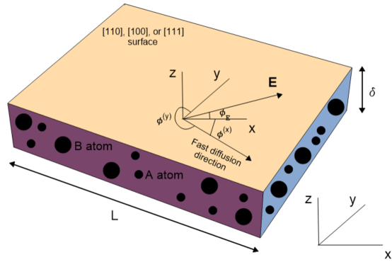
We consider a compositionally nonuniform binary metal layer (a substitutional binary alloy) of a constant thickness , annealed at high temperature. The layer may represent either the surface layer of a surface alloy film, or the ultrathin alloy film on a thick conductive substrate. We refer to this setup simply as film. Two atomic components of the film are denoted as A and B. The electric potential difference (voltage) is applied to the opposite edges of the substrate, which results in the electric field (Fig. 1). Here is the width of the substrate between the anode and the cathode, and also the horizontal film dimension, and the angle that the electric field vector makes with the -axis of the Cartesian reference frame (the direction angle). and axes are in the film/substrate plane, and the axis is perpendicular to that plane, and it points into the vapor or vacuum above the film. The electric current through the film activates electromigration. The film thickness is assumed small, i.e. on the order of several atomic diameters TersoffAlloy . For computations we chose equal to two diameters of a Pd atom (Table 1). Due to small film thickness and to the planar geometry of the electric field, the diffusion and electromigration mass flows along the -axis are negligible and thus they are not considered by the model. Computations in Sec. III will be done for CuPd alloy; this alloy is often used in electromigration experiments PV .
Let and be the number of atoms of the components A and B per substrate area. Then the dimensionless concentrations, or the local composition fractions, are defined as and , where . Clearly,
| (1) |
where is the time. Physically, this condition stems from the negligible vacancy concentration in a substitutional alloy. In the remainder of this section we construct a diffusion/electromigration model that enables to follow the spatio-temporal evolution of . Notice that this is sufficient, since due to Eq. (1) the evolution of follows trivially from equation (thus if increases locally, i.e. at some point in the film, then decreases at that point with the same rate).
The diffusion equation reads
| (2) |
where is the atomic volume and . Since the mass transport is driven by the gradient of the chemical potential and by electromigration, the flux is given by
| (3) |
where is the diffusion tensor, the Boltzmann’s factor, and the effective charge.
The chemical potential in Eq. (3) is the sum of the contributions due to alloy thermodynamics and the compositional stress ZVD ; SVT ; RSN :
| (4) |
where is the free energy, the Cahn-Hilliard gradient energy coefficient, the effective solute expansion coefficient, and . The effective solute expansion coefficient measures the relative size difference of A and B atoms and quantifies the linear lattice strain due to increasing the concentration of B. corresponds to large B atoms. Choosing or depends on whether the compositional stress is compressive or tensile. When the stress is tensile and , the destabilization of the base uniform composition state is expected SVT . The linear stability analysis (LSA, see below) shows that for the average typical film composition the destabilization occurs at . Therefore this value corresponds to the tensile stress, and it is chosen for the remainder of this section and for computations in Sec. III.
The free energy in Eq. (4) is written as RSN ; LuKim :
| (5) |
where and are the energies of pure A and B on the substrate surface, is the alloy entropy, and the dimensionless number measures the bond strength relative to the thermal energy . Here is the enthalpy. The first two terms are needed since the film thickness is on the order of a few atomic diameters, and the terms in the bracket are the regular solution model. When , the graph of is a double-well curve, which results in spinodal decomposition. For simulations we chose value (see Table 1) such that and the -curve is convex, thus spinodal instability is absent and the only source of instability is the compositional stress, again refer to the LSA below.444Experimental conditions are possible when the spinodal instability is present alongside with the compositional stress instability. Computations of compositional patterning in such situation in the absence of electromigration can be found in Ref. KH1 . Generally, phase separation is enhanced, i.e. it develops faster and the resultant composition differences are larger, when two instabilities act simultaneously.
Finally, the diffusivity, , is given by a transversely isotropic diffusion tensor
| (6) |
where , are the surface diffusional anisotropy functions for face-centered cubic (fcc) crystals DM ; DM1 . is the strength of crystallographic anisotropy and () are the misorientation angles formed between the -axis and the fast surface diffusion direction. Note that (are positive). The integer is determined by the crystallographic orientation of the film surface. For ([110] surface): , ; for ([100] surface): , ; for ([111] surface): , DM . See Refs. DM ; KH1 for plots of and .
Combining equations, using the typical thickness of the as-deposited surface alloy film as the length scale and as the time scale, yields the dimensionless PDE for :
| (7) |
where
| (8) |
The dimensionless parameters are the ratio of the pure energies , the entropy , the enthalpy , the Cahn-Hilliard gradient energy coefficient , the solute expansion coefficient , and the electric field strength that enters the effective “anisotropic” electric field vector . Also is the anisotropic gradient operator, where is the dimensionless ratio of the amplitudes of the diagonal components of the anisotropic diffusivity tensor. We will call the diffusional anisotropy. At the diffusional anisotropy is zero.555Of course, the separation into crystallographic and diffusional anisotropy is only for convenience of discussion. Both anisotropies stem from the anisotropy of diffusion in the surface layer of a single-crystal film, see Eq. (6). may be as large as 1000, and as small as 0.001 if the atomic rows happen to run along one of the two coordinate axes, say the -axis (and correspondingly, the -axis is orthogonal to the rows). This is because the diffusion across the rows requires an activation energy that is at least three times larger than the activation energy for the diffusion along the rows ES ; MG .
It is clear that the second term in Eq. (7) describes the forced mass transport due to electromigration effect. Including and the angles , there is ten parameters (nine if ), since is defined through .666Notice that when (Table 1); in this situation the number of dimensionless parameters can be reduced from nine to eight, since can be made equal to one via replacing by in the definitions of the remaining parameters.
Remark 1. Setting amounts to consideration of a generic film surface with the diffusional anisotropy, since in this case the crystallographic parameters , and are irrelevant. Note that and . It follows that if in addition to , then the diffusion tensor is isotropic, with identical diagonal components (, where is the diffusivity and the identity tensor), and also . In this case there is complete isotropy.
Remark 2. When the crystallographic anisotropy strength , the anisotropic gradient operator even at zero diffusional anisotropy, due to intrinsic reconstruction of a particular low-index crystal surface. The overall anisotropy effect is enhanced if in addition to crystallographic anisotropy the diffusional anisotropy is also present.
Remark 3. As derived, the electromigration term should be . Based on many simulations we realized that multiplication by a ”volume exclusion” factor is necessary in order to ensure stable computation. The factor is due to the fact that the diffusion flow can only pass through the available vacant sites (a finite occupancy effect). We later found that this factor can be transparently derived by scaling to continuum limit the discrete-space, continuous-time equation for the density of diffusing, size-zero particles on a lattice P . In the field of materials modeling, this factor can be seen, for example, in the forcing terms of the diffusion equations in Refs. CTT ; KDB ; KK .
Remark 4. Eq. (7) has been developed in the general spirit of a model for the dynamics of a composition of a binary monolayer, developed by Z. Suo’s group; see Ref. LuKim and the references therein.
The standard LSA of Eq. (7) about composition yields the complex perturbation growth rate , where and are the perturbation wavenumbers in the and directions, and
| (9) | |||||
| (10) |
with
| (11) |
At (the choice for the computation in Sec. III), the last two terms in evaluate to -0.0033 at the parameters from Table 1, and since due to for CuPd alloy; thus , and at the positive and terms in contribute to growth of small wavenumbers, while the negative terms proportional to contribute to the decay of large wavenumbers. Note that value of that corresponds to Table 1 parameters is 0.015. Thus the linear instability displayed by has the long-wavelength character. The imaginary part of the growth rate, is not zero only when the electric field parameter . Note that does not depend on the compositional stress or on alloy thermodynamic parameters and , and also that the anisotropies affect values of both and . In the presence of the electromigration a perturbation drifts in the -plane with the speed (a traveling wave). This drift in the nonlinear regime may influence the pattern formation.777The electromigration-driven surface waves were analyzed by Bradley in a model of a morphology evolution for a single-component film B1 ; B2 ; B3 . Note that the compositional stress contribution in , and the drift, both vanish at , i.e. at the perfectly balanced average layer composition, 50%A/50%B.
Fig. 2 shows the plots of . The maximum value occurs at . When the parameters , , , and change within the intervals of interest in Sec. III, these plots experience only minor changes, and thus value changes insignificantly. This value sets the size of the (square) computational domain, .

| Physical parameter | Typical value |
|---|---|
| cm (500 nm) | |
| cm (0.676 nm) | |
| cm-2 ZVD ; LuKim | |
| cm3 | |
| 923 K | |
| statC YTRW | |
| V | |
| ergcm2 | |
| , | ergcm2 VRSK |
| ergcm Hoyt | |
| ergcm3 SVT |
III Formation and evolution of composition patterns
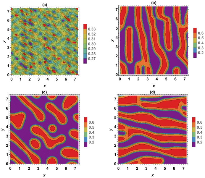
In this section we present the results of computations with Eq. (7). In all computations we use the initial condition , where is a random deviation from the mean value 0.3 with the maximum amplitude 0.08 at a point (Fig. 3(a)). We employ the method of lines framework with a pseudospectral spatial discretization on 140x140 rectangular grid and a stiff ODE solver in time. Periodic conditions are imposed on the boundary of a square computational domain. We fix the physical parameters to their values in Table 1, and systematically vary the direction angle of the electric field , the diffusional anisotropy (both at the zero crystallographic anisotropy), and the crystallographic orientation of the surface (at the fixed non-zero strength of the crystallographic anisotropy, DM , at zero diffusional anisotropy, and at fixed ). This is in order to transparently separate, and thus understand, the effects of both anisotropies and of the electric field direction angle. Also, for [110] surface (), we compute the “full” case, i.e. at both anisotropies present and with the fixed direction angle of the electric field, and varying the misorientation “diffusion” angle . And finally, we fix in the full case and study the effect of the electric field strength by moderately varying applied voltage . Note that by the choice of the electric field parameter is rather small, so that forced mass transport due to electromigration competes with the natural diffusion.
III.1 Zero electric field
When the external electric field is off, the composition patterns in the thin film are disordered. Fig. 3(b-d) shows as the example the late time composition patterns at and . In this case different patterns arise solely due to diffusional anisotropy, see Remarks 1 and 2 in Sec. II. As expected, at (i.e., when the diffusion strengths in the and direction are the same, ), and the spatial rates of change in the and directions are given by and , thus the spatial variations in the pattern are similar in both directions. At , the rate of change in the -direction is roughly 10 times smaller than in the -direction, thus the pattern looks more uniform in the -direction than in the -direction, i.e. the changes in the form of the alternation of small and large occur primarily in the -direction. The overall effect is the pattern that consists of a worm-like, often “zipped” (forked) bands of alternating large/small content (red/purple colored) running in the direction. At the situation is reversed. Note that the final dimensionless time in Fig. 3(b-d) corresponds to the physical time of 28 min, assuming the typical surface diffusivity value cms at K AKR .
III.2 Non-zero electric field
III.2.1 Non-zero crystallographic anisotropy, zero diffusional anisotropy:
In this subsection we summarize composition patterns in the films of three chosen crystallographic orientations as a function of the direction angle of the electric field, .
-
1.
or .
These electric field directions are not equivalent when there is a coupling to the crystallographic anisotropy, as follows from the definition of the effective electric field vector , see Sec. II. In [110]-oriented film (), both electric field directions result in the perfect stripe pattern whose axis is parallel to the axis (Fig. 4(a)). This is also the case at and [100]-oriented film (). At all other combinations of two values and three values there still is the orientation effect of the electric field, i.e. the field tries to align the pattern axis with the -axis, however, the stripes do not emerge. At any time during the evolution, there emerge instead the multiple-connected domains, see Fig. 4(b).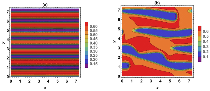
Figure 4: Examples of composition patterns. at and (a): , (b): . See Sec. III.2.1, item 1 for discussion. -
2.
or .
This situation is similar to item 1 in this list. There is either the vertical stripes (Fig. 5), or the multiple-connected domains loosely aligned with the -axis. Notice that the aerial number density of stripes, when checked at the same time, varies with the crystallographic orientation.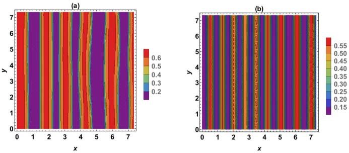
Figure 5: Examples of composition patterns. at and (a): , (b): . See Sec. III.2.1, item 2 for discussion. -
3.
or .
For these tilted electric field directions the ordered stripe pattern emerges only at [100] surface orientation, , and the stripes also make the field-imposed angle with the -axis, see Fig. 6(a-c). For other surface orientations the stripe pattern is not perfect at computed times. For instance, in Fig. 6(d) one can notice zipped stripes, and the angle that these stripes make with the axis may significantly deviate from - more so as computed evolution gets longer. Fig. 6(a-c) shows the time-progression of the coarsening of the perfect stripe pattern, i.e. the reduction of the aerial number density of the stripes with a high content (red stripes). Note that the number of red stripes is reduced from 14 in Fig. 6(a) to 8 in Fig. 6(c). Fig. 6(b) captures the moment when some red stripes are dissolving, which increases the width of low content purple stripes.Remark 5. Some coarsening is present for all cases computed in this paper, but we stopped short of quantitatively characterizing this process, since this requires computing on very long time scales. We presently do not possess the computational resources for this task. It is important to underscore that a perfect stripe pattern always emerges at the early stages in the evolution and it stays perfect regardless of the coarsening rate. However, a multiple-connected domains pattern never transforms into a perfect stripe pattern at later times, and a zipped stripe pattern, such as one in Fig. 6(d), infrequently becomes a perfect stripe pattern at very large times.
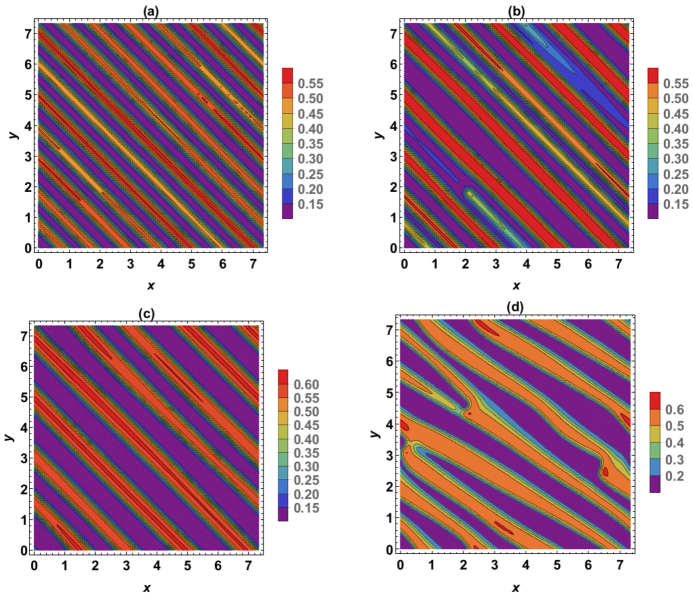
Figure 6: Examples of composition patterns. (a-c): at and . (d): at and . See Sec. III.2.1, item 3 for discussion.
III.2.2 Zero crystallographic anisotropy, non-zero diffusional anisotropy:
In this subsection the crystallographic anisotropy is zero, thus values of and are irrelevant. We summarize the patterns at various direction angles of the electric field, , and at various diffusional anisotropies .
-
1.
or .
Horizontal stripe pattern at , and multiple-connected domains at . For the aerial number density decreases as increases. -
2.
or .
Disordered pattern at (similar to Fig. 3(b)); perfect vertical stripes at . The aerial number density depends on non-monotonously, first decreasing at and then increasing at and reaching the maximum value of 7 or 8 (Fig. 7(a)). The times of the stripe pattern formation, , shown in Fig. 7(b) decrease rapidly as increases, reach the minimum value 1000 at , and stay constant as further increases.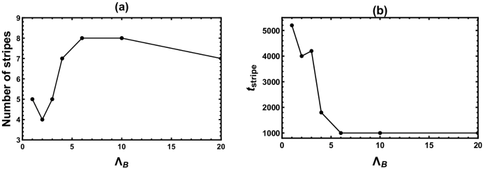
Figure 7: (a): The number of vertical stripes vs. . For each value shown, the stripes are counted when the stripe pattern first emerges. These times are plotted in (b) vs. . See Sec. III.2.2, item 2 for discussion. -
3.
or .
Zipped stripe pattern at , transforming into a perfect stripe pattern at . The aerial number density increases as increases for , and decreases as increases for . Stripes become more vertical as increases, see Fig. 8 (thus the pattern orientation angle deviates from for ).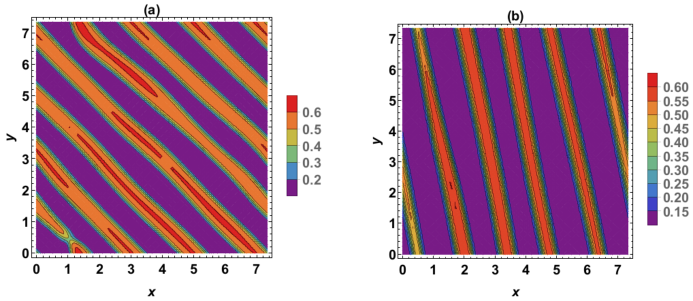
Figure 8: Examples of composition patterns. at and (a): , (b): . See Sec. III.2.2, item 3 for discussion.
III.2.3 Crystallographic anisotropy and diffusional anisotropy both non-zero:
In this subsection we discuss the computation of the composition evolution in [110]-oriented film with the full anisotropy effect. Such situation is most relevant to experiment.
Fig. 9 shows the impact of the diffusion misorientation angle . The competition of the electric field and the anisotropy is very striking. The electric field tries to align the stripe pattern at angle to the axis, but the diffusion anisotropy interferes, and only at the angle is achieved. It may be said that at the anisotropy and the electric field are aligned, creating the “constructive interference effect”. Conversely, at , unlike at other values, the stripe pattern is double-zipped - the misalignment between the electric field and the anisotropy creates the “destructive interference effect”. (Notice also that at the stripes are present, but they are not straight and their inclination angle to the -axis is larger than .) Between these two extremes, the stripe inclination angle reflects the balance between and , and the aerial number density of the stripes is also affected by how close are these angles. It is the largest at and , i.e. when deviates the most from .
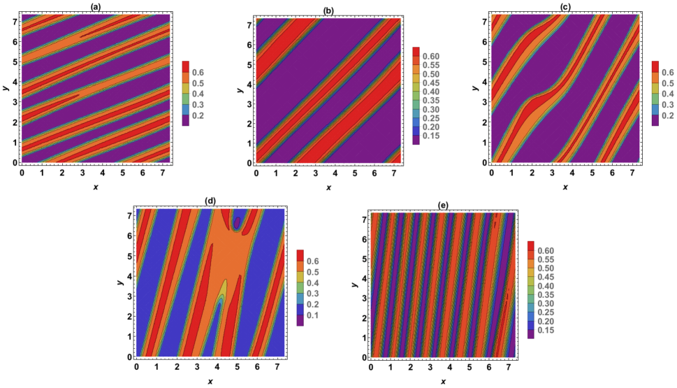
It is important to emphasize here that also for [100] and [111]-oriented films there does exist a combination of the parameters ensuring that the stripes form in the electric field direction. For instance, in [111] case, keeping , the stripes form at angle to the axis provided that .
Lastly, Fig. 10 shows the impact of the last parameter that remains to study - the applied voltage . We chose all parameters as in Fig. 9(d) and increased . It is obvious that at higher voltage the quality of the stripe pattern is improved. Another effect is the increased aerial number density. However, the alignment to the electric field direction, , does not improve when the electromigration effect gets stronger. Increasing beyond V we did not detect any further changes to the pattern that is shown in Fig. 10(c). It is worth observing that these results transparently show that the aerial number density (equivalently, the wavelength of the 1D spatially periodic stripe pattern) is unrelated to the LSA most dangerous wavelength 888, where , and maximize ., since the latter wavelength stems from the real part of the perturbation growth rate, whereas enters only the imaginary part of that rate. Thus the aerial number density should be determined by the nonlinear interaction of the lateral concentration waves.

Based on the computations in this section, for the most practical [110] surface orientation with the mild total anisotropy, , and at a fixed electric field strength the stripes angle satisfies , where is the positive function that attains a minimum on its domain . Here and are the positive angles, such that is in the same quadrant with . The aerial number density of the stripes is the largest at the endpoints and . Increasing the strength of the applied electric field below a certain upper limit (while keeping and fixed) eliminates the imperfect stripes, increases the aerial number density of the perfect ones, and shortens the formation time of a perfect stripe pattern.
IV Summary
We demonstrated how the complex interaction of the diffusion and electromigration influences the formation and evolution of the stripe composition patterns in a thin, crystallographically oriented surface layer of a heated substitutional binary alloy film. With a full surface diffusion anisotropy, there is no single control parameter that is responsible for both the stripes alignment to the electric field direction and for the aerial number density of the stripes. Tuning the applied voltage allows to adjust the density, and tuning the electric field direction allows to form the stripes that are closely aligned to that direction. If the anisotropy parameters are certain, then the computer simulation of this model would inform the experiment about the expected pattern.
References
- (1) R. Yongsunthon, C. Tao, P. Rous, and E.D. Williams, “Surface electromigration and current crowding”, Chapter 5 in: Nanophenomena at Surfaces: Fundamentals of Exotic Condensed Matter Properties, Ed. M. Michailov, Springer (2011).
- (2) C. Tao, W.G. Cullen, and E. D. Williams, “Visualizing the electron scattering force in nanostructures”, Science 328, 736 (2010).
- (3) L. Valladares, L.L. Felix, A.B. Dominguez, T. Mitrelias, F. Sfigakis, S.I. Khondaker, C.H.W. Barnes, and Y. Majima, “Controlled electroplating and electromigration in nickel electrodes for nanogap formation”, Nanotechnology 21, 445304 (2010).
- (4) G. Gardinowski, J. Schmeidel, H. Phnur, T. Block, and C. Tegenkamp, “Switchable nanometer contacts: Ultrathin Ag nanostructures on Si(100)”, Appl. Phys. Lett. 89, 063120 (2006).
- (5) S. Curiotto, P. Muller, A. El-Barraj, F. Cheynis, O. Pierre-Louis, and F. Leroy, “2D nanostructure motion on anisotropic surfaces controlled by electromigration”, Appl. Surf. Sci. 469, 463-470 (2019).
- (6) J. Zhao, R. Yu, S. Dai, and J. Zhu, “Kinetical faceting of the low index W surfaces under electrical current”, Surf. Sci. 625, 10 (2014).
- (7) S. Stoyanov, “Current-induced step bunching at vicinal surfaces during crystal sublimation”, Surf. Sci. 370, 345 (1997).
- (8) M. Dufay, J.-M. Debierre, and T. Frisch, “Electromigration-induced step meandering on vicinal surfaces: Nonlinear evolution equation”, Phys. Rev. B 75, 045413 (2007).
- (9) J. Chang, O. Pierre-Louis, and C. Misbah, “Birth and morphological evolution of step bunches under electromigration”, Phys. Rev. Lett. 96, 195901 (2006).
- (10) O. Pierre-Louis, “Local electromigration model for crystal surfaces”, Phys. Rev. Lett. 96, 135901 (2006).
- (11) J. Krug and H.T. Dobbs, “Current-induced faceting of crystal surfaces”, Phys. Rev. Lett. 73, 1947 (1994).
- (12) M. Schimschak and J. Krug, “Surface electromigration as a moving boundary value problem”, Phys. Rev. Lett. 78, 278 (1997).
- (13) D. Du and D. Srolovitz, “Electrostatic field-induced surface instability”, Appl. Phys. Lett. 85, 4917 (2004).
- (14) F. Barakat, K. Martens, and O. Pierre-Louis, “Nonlinear wavelength selection in surface faceting under electromigration”, Phys. Rev. Lett. 109, 056101 (2012).
- (15) C.-H. Chiu, Z. Huang, and C. T. Poh, “Formation of nanoislands by the electromolding self-organization process”, Phys. Rev. B 73, 193409 (2006).
- (16) D. Maroudas, “Surface morphological response of crystalline solids to mechanical stresses and electric fields”, Surf. Sci. Reports 66, 299 (2011).
- (17) V. Tomar, M.R. Gungor, and D. Maroudas, “Current-induced stabilization of surface morphology in stressed solids”, Phys. Rev. Lett. 100, 036106 (2008).
- (18) T.O. Ogurtani, “The orientation dependent electromigration induced healing on the surface cracks and roughness caused by the uniaxial compressive stresses in single crystal metallic thin films”, J. Appl. Phys. 105, 053503 (2009).
- (19) M. Khenner, “Analysis of a combined influence of substrate wetting and surface electromigration on a thin film stability and dynamical morphologies”, C. R. Physique 14, 607 (2013).
- (20) J.H. Kim, D.J. Srolovitz, P.-R. Cha, and J.K. Yoon, “Capillarity and electromigration effects on asperity contact evolution in microelectromechanical systems switches”, J. Appl. Phys. 100, 054502 (2006).
- (21) L. Du and D. Maroudas, “Optimization of electrical treatment strategy for surface roughness reduction in conducting thin films”, J. Appl. Phys. 124, 125302 (2018).
- (22) P. Kuhn, J. Krug, F. Hausser, and A. Voigt, “Complex Shape Evolution of Electromigration-Driven Single-Layer Islands”, Phys. Rev. Lett. 94, 166105 (2005).
- (23) D. Dasgupta and D. Maroudas, “Surface nanopatterning from current-driven assembly of single-layer epitaxial islands”, Appl. Phys. Lett. 103, 181602 (2013).
- (24) D. Dasgupta, A. Kumar, and D. Maroudas, “Analysis of current-driven oscillatory dynamics of single-layer homoepitaxial islands on crystalline conducting substrates”, Surf. Sci. 669, 25 (2018).
- (25) A. Kumar, D. Dasgupta, C. Dimitrakopoulos, and D. Maroudas, “Current-driven nanowire formation on surfaces of crystalline conducting substrates”, Appl. Phys. Lett. 108, 193109 (2016).
- (26) D. Solenov and K.A. Velizhanin, “Adsorbate transport on graphene by electromigration”, Phys. Rev. Lett. 109, 095504 (2012).
- (27) R. Spolenak, O. Kraft, and E. Arzt, “Effects of alloying elements on electromigration”, Microelectronics Reliability 38, 1015 (1998).
- (28) Y.-J. Park, V.K. Andleigh, and C.V. Thompson, “Simulations of stress evolution and the current density scaling of electromigration-induced failure times in pure and alloyed interconnects”, J. Appl. Phys. 85, 3546 (1999).
- (29) J. P. Dekker, C.A. Volkert, E. Arzt, and P. Gumbsch, “Alloying effects on electromigration mass transport”, Phys. Rev. Lett. 87, 035901 (2001).
- (30) S. Yokogawa and H. Tsuchiya, “Effects of Al doping on the electromigration performance of damascene Cu interconnects”, J. Appl. Phys. 101, 013513 (2007).
- (31) F. Besenbacher, L.P. Nielsen, and P.T. Sprunger, “Surface alloying in heteroepitaxial metal-on-metal growth”, in: The Chemical Physics of Solid Surfaces, Ed.: D.A. King and D.P. Woodruff, vol. 8, Elsevier (1997).
- (32) G.L. Kellogg, “Surface alloying and de-alloying of Pb on single-crystal Cu surfaces”, in: The Chemical Physics of Solid Surfaces, Ed.: D.P. Woodruff, vol. 10, Elsevier (2002).
- (33) J. Tersoff, “Surface-confined alloy formation in immiscible systems”, Phys. Rev. Lett. 74, 434 (1995).
- (34) C.W. Park and R.W. Vook, “Electromigration-resistant Cu-Pd alloy films”, Thin Solid Films 226, 238-247 (1993).
- (35) Q. Zhang, P.W. Voorhees, and S.H. Davis, “Mechanisms of surface alloy segregation on faceted core-shell nanowire growth”, J. Mech. Phys. Solids 100, 21-44 (2017).
- (36) B.J. Spencer, P.W. Voorhees, and J. Tersoff, “Morphological instability theory for strained alloy film growth: The effect of compositional stresses and species-dependent surface mobilities on ripple formation during epitaxial film deposition”, Phys. Rev. B 64, 235318 (2001).
- (37) A.V. Ruban, H.L. Skriver, and J.K. Norskov, “Local equilibrium properties of metallic surface alloys”, in: The Chemical Physics of Solid Surfaces, Ed.: D.P. Woodruff, vol. 10, Elsevier (2002).
- (38) W. Lu and D. Kim, “Engineering nanophase self-assembly with elastic field”, Acta Mater. 53, 3689 (2005).
- (39) L. Du and D. Maroudas, “Theory of multiple quantum dot formation in strained-layer heteroepitaxy”, Appl. Phys. Lett. 109, 023103 (2016).
- (40) M. Khenner and V. Henner, “Modeling composition patterns in a binary surface alloy”, submitted.
- (41) G. Ehrlich and K. Stolt, “Surface diffusion”, Annu. Rev. Phys. Chem. 31, 603 (1980).
- (42) Y.-W. Mo and M.G. Lagally, “Anisotropy in surface migration of Si and Ge on Si(001)”, Surf. Sci. 248, 313 (1991).
- (43) K.J. Painter, “Continuous models for cell migration in tissues and applications to cell sorting via differential chemotaxis”, Bull. Math. Biology 71, 1117 (2009).
- (44) M.G. Clerc, E. Tirapegui, and M. Trejo, “Pattern formation and localized structures in reaction-diffusion systems with non-Fickian transport”, Phys. Rev. Lett. 97, 176102 (2006).
- (45) V.O. Kharchenko, A.V. Dvornichenko, and V.N. Borysiuk, “Formation of adsorbate structures induced by electric field in plasma-condensate systems”, Eur. Phys. J. B 91, 93 (2018).
- (46) A.P. Krekhov and L. Kramer, “Phase separation in the presence of spatially periodic forcing”, Phys. Rev. E 70, 061801 (2004).
- (47) L. Vitos, A.V. Ruban, H.L. Skriver, and J. Kolla, “The surface energy of metals”, Surf. Sci. 411, 186-202 (1998).
- (48) J.J. Hoyt, “Molecular dynamics study of equilibrium concentration profiles and the gradient energy coefficient in Cu-Pb nanodroplets”, Phys. Rev. B 76, 094102 (2007).
- (49) E. Clementi, D.L. Raimondi, and W.P. Reinhardt, “Atomic Screening Constants from SCF Functions. II. Atoms with 37 to 86 Electrons”, J. Chem. Phys. 47, 1300 (1967).
- (50) D. Amram, L. Klinger, and E. Rabkin, “Anisotropic hole growth during solid-state dewetting of single-crystal Au-Fe thin films”, Acta Mater. 60, 3047-3056 (2012).
- (51) M. Khenner and M. Bandegi, “Electromigration-driven evolution of the surface morphology and composition for a bi-component solid film”, Math. Modell. Nat. Phenom. 10, 83 (2015).
- (52) R.M. Bradley, “Electromigration-induced propagation of nonlinear surface waves”, Phys. Rev. E 65, 036603 (2002).
- (53) R.M. Bradley, “Electromigration-induced shock waves on metal thin films”, Appl. Phys. Lett. 93, 213105 (2008).
- (54) R.M. Bradley, “Shock waves on current-carrying metal thin films”, Phys. Rev. B 79, 075403 (2009).