Magneto-Seebeck microscopy of domain switching in collinear antiferromagnet CuMnAs
Antiferromagnets offer spintronic device characteristics unparalleled in ferromagnets owing to their lack of stray fields, THz spin dynamics, and rich materials landscape. Microscopic imaging of antiferromagnetic domains is one of the key prerequisites for understanding physical principles of the device operation. However, adapting common magnetometry techniques to the dipolar-field-free antiferromagnets has been a major challenge. Here we demonstrate in a collinear antiferromagnet a thermoelectric detection method by combining the magneto-Seebeck effect with local heat gradients generated by scanning far-field or near-field techniques. In a 20 nm epilayer of uniaxial CuMnAs we observe reversible 180∘ switching of the Néel vector via domain wall displacement, controlled by the polarity of the current pulses. We also image polarity-dependent 90∘ switching of the Néel vector in a thicker biaxial film, and domain shattering induced at higher pulse amplitudes. The antiferromagnetic domain maps obtained by our laboratory technique are compared to measurements by the established synchrotron-based technique of x-ray photoemission electron microscopy using X-ray magnetic linear dichroism.
Writing and reading by electrical and optical means, high speed operation combined with neuromorphic memory characteristics, and novel topological phenomena are among the topics that have driven the research in the emerging field of antiferromagnetic spintronics Jungwirth2016 ; Baltz2018 ; Zelezny2018 ; Gomonay2018 ; Nemec2018 ; Smejkal2018 . The development of devices whose operation is based on antiferromagnets was initiated by theoretical predictions Shick2010 ; Zelezny2014 and subsequent experimental demonstrations of electrical detection and manipulation of the antiferromagnetic order by relativistic anisotropic magnetoresistance (AMR) and Néel spin-orbit torque (NSOT) effects in metallic antiferromagnetsPark2011b ; Marti2014 ; Wadley2016 ; Godinho2018 . From the early days of the antiferromagnetic spintronics research, a special attention is paid to complementing these electrical measurements by direct microscopic imaging of the typically multidomain states of the studied antiferromagnets Wadley2016 ; Grzybowski2017 ; Wadley2018 ; Moriyama2018 ; Reichlova2019 ; Gray2019 ; Bodnar2019 ; Baldrati2019 ; Wornle2019 ; Kaspar2019 . The aim of these microscopies is to elucidate physical mechanisms of the switching which, e.g., in CuMnAs have been associated with the Néel vector reorientation induced by the NSOT, and with electrical or optical pulse-induced quenching into paidnano-fragmented domain states of the antiferromagnetWornle2019 ; Kaspar2019 . The microscopies are also essential for disentangling potential parasitic non-magnetic contributions to the resistive switching signals, as reported in metal/antiferromagnetic-insulator bilayersChiang2019 ; Zink2019 ; Zhang2019c ; Baldrati2019 ; Cheng2020 ; Churikova2020 .
However, established microscopy techniques for imaging antiferromagnets are rare and rely primarily on large-scale experimental facilities. Among these, X-ray magnetic linear dichroism combined with photoemission electron microscopy (XMLD-PEEM) Scholl2000 was used to visualize the electrical control of the Néel vector in CuMnAs, Mn2Au, or NiO Wadley2016 ; Grzybowski2017 ; Wadley2018 ; Moriyama2018 ; Bodnar2019 ; Baldrati2019 . In CuMnAs, the XMLD-PEEM images of the onset of current-induced NSOT reorientation of the Néel vector were directly linked to the onset of the corresponding electrical readout signals due to AMR Grzybowski2017 ; Wadley2018 . 90∘ Néel vector switching was observed by XMLD-PEEM for orthogonal writing currents Wadley2016 ; Grzybowski2017 or, via domain wall motion, when reversing the polarity of the writing current Wadley2018 . Since XMLD-PEEM is a synchrotron-based technique, more accessible table-top microscopies are necessary for a systematic exploration of antiferromagnetic devices. An example here is the NV-diamond magnetometryDegen2008 ; Balasubramanian2008 which was recently reported in antiferromagnetic Cr2O3, BiFeO3, and CuMnAs Kosub2016 ; Gross2017 ; Wornle2019 , and which relies on stray-fields generated by uncompensated magnetic moments.
In this work we investigate current pulse-induced changes of the domain structure in the compensated collinear antiferromagnet CuMnAsWadley2013 ; Wadley2015a , focusing on 90∘ and 180∘ Néel vector switching as well as domain fragmentation. For the microscopic imaging we utilize a thermoelectric response due to the magneto-Seebeck effect (MSE), which is a thermal analog of AMR. The MSE can be applied to the large class of conductive antiferromagnets and is not limited to either uncompensated antiferromagnets that still produce detectable magnetic stray fields, or to systems whose additional broken symmetries allow for the anomalous Nernst effect or the magnetooptical Kerr effect, such as non-collinear antiferromagnets.
The MSE response is mapped to a laser-induced localized temperature gradient in the device. A thermoelectric voltage signal is measured across the entire bar device when the scanning probe is placed on top of an antiferromagnetic texture with spatially varying Néel vector.
We employ two techniques: The first one is based on the scanning far-field optical microscopy (SFOM) Weiler2012 , which in combination with anomalous Nernst or spin-Seebeck thermoelectric response was employed in earlier studies of a non-collinear antiferromagnet Mn3Sn and a metal/antiferromagnetic-insulator bilayer Pt/NiO, respectively Reichlova2019 ; Gray2019 . In the second, high-resolution approach we utilize photocurrent nanoscopy in a scattering-type scanning near-field optical microscope (SNOM) Pfitzner2018 ; Woessner2016 ; Lundeberg2017 . Here a metal-coated tip of an atomic force microscope (AFM) placed in close proximity to the CuMnAs surface acts as an optical antenna for light focused on the tip. The incident electric field is strongly confined around the tip apex, providing a nanoscale near field point source. Since, to the best of our knowledge, the scanning optical microscopy combined with MSE has not been applied to antiferromagnets prior to our work, we provide comparisons to images obtained by the established synchrotron XMLD-PEEM technique.
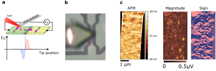
Comparison of optical-thermoelectric and X-ray microscopies of CuMnAs domains
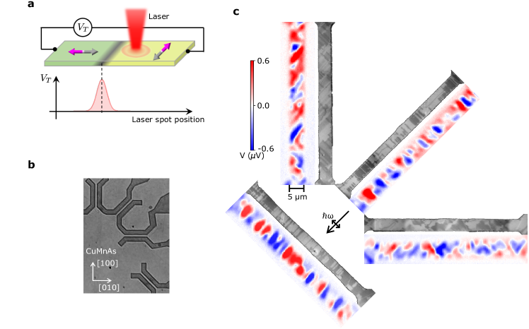
In Fig. 1a we illustrate our SFOM-MSE technique on two neighbouring antiferromagnetic domains separated by a 90∘ domain wall. We use a 800 nm wavelength cw-laser beam of 1 mW power focused to a spot with a full-width at half-maximum (FWHM) of m on the surface of the CuMnAs antiferromagnet. The laser spot generates a lateral radially symmetric temperature gradient and we monitor the laser-induced thermoelectric voltage, , at the two ends of the bar device. Non-zero may occur when the temperature gradient crosses an antiferromagnetic domain boundary, as shown schematically in Fig. 1a. This is because the Néel vector reorients and, therefore, the magneto-Seebeck coefficient changes Krzysteczko2015 so that the net thermoelectric signal does not cancel. As we show in the Supplementary Note 1, we can reproduce the sign and magnitude of the measured signal with a magneto-Seebeck coefficient V/K by considering the boundary conditions of our open circuit configuration, thermal conductivities of 200 W/(Km) and 75 W/(Km) for the metallic CuMnAs film and for the insulating GaP substrate, respectively, and by assuming that of the laser power is absorbed within the metallic CuMnAs layer. Here () is the Seebeck coefficient when the Néel vector is collinear (perpendicular) to the temperature gradient. Note that the calculated maximum temperature rise at 5 mW laser power, the highest power used in our SFOM-MSE experiments, is not greater than 6 K (see Supplementary Note 1). We also verified that anisotropies of the conductivity, e.g., due to AMR, give a negligible contribution to the thermoelectric voltage signal.
The optical micrograph in Fig. 1b shows four 50 m long and 5 m wide bars, which were patterned from a 45 nm thick CuMnAs/GaP epilayer Wadley2013 ; Wadley2018 along [100], [10], [110] and [010] crystallographic axes of CuMnAs. The SFOM-MSE signals of the four devices are compared in Fig. 1c to the XMLD-PEEM measurements taken on the same bars with X-ray polarization crystal axis. The light and dark areas correspond to antiferromagnetic domains with the Néel vector oriented perpendicular and parallel to the X-ray polarization, respectivelyWadley2016 ; Wadley2018 . Both domains with orthogonal orientation are found in our 45 nm thick CuMnAs film with the dominant in-plane biaxial magnetic anisotropy Wadley2018 .
The SFOM-MSE and the XMLD-PEEM measurements show analogous structures of micron-scale domains in each of the four bars. The preferential alignment of the domain walls follows the crystallographic directions of the in-plane square lattice of CuMnAs. This results in the 45∘ rotation of the preferred domain wall alignment with respect to the bar edges between the [100] ([010]) and [10] ([110]) bars.
The analogous overall structure of the SFOM-MSE and XMLD-PEEM images confirms that the main contribution to the thermoelectric voltage signal comes from the antiferromagnetic texture and the corresponding variation of the magneto-Seebeck coefficient. Quantitative differences between the two measurements can be ascribed to different lateral resolution and depth sensitivity of the two techniques. The lateral resolution of the XMLD-PEEM in the metallic antiferromagnet CuMnAs is about 50 nm while the resolution of the SFOM-MSE is limited by the thermal gradient generated by the m wide Gaussian shaped laser spot. Regarding the depth sensitivity, the photo-electrons in the XMLD-PEEM are detected only from a few-nm surface layer of the antiferromagnet while the thermoelectric measurements probe the full thickness of the antiferromagnetic film. Note also that the XMLD-PEEM measurements were performed about 10 days before the SFOM-MSE measurements.
Optical thermoelectric imaging of the current-induced switching
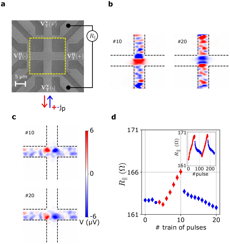
We now use the SFOM method to correlate the local magnetic domain structure to electrical resistance variation after current pulse excitation, which further evidences that the image contrast we detect is indeed of magnetic origin. We simultaneously measure the thermoelectric signals along the vertical and horizontal bars in a symmetric m wide cross bar geometry, shown in Fig. 2a . The vertical and horizontal SFOM-MSE voltages and in Fig. 2a are recorded while scanning the focused laser spot over the central crossbar structure, highlighted in Fig. 2a by the dashed yellow rectangle.
Figures 2b,c show the corresponding maps after trains of positive and negative current pulses were applied along the vertical bar with amplitude A/m2 and duration ms. Vertical and horizontal thermoelectric signals reflect a complex microscopic domain structure. They appear only when the scanning laser spot illuminates the corresponding bars. After the applied vertical current pulses, variations of the vertical signal were observed along the entire vertical bar, whereas the horizontal signal changes only in the central overlapping crossbar region. These measurements confirm Current-pulse-induced switching of the microscopic domain structure since modifications of the thermoelectric signal occur only in areas where the current density of the applied pulse was sufficiently large to trigger the switching Wadley2018 .
Figure 2d shows the electrical resistance, , measured in a 4-point geometry after applying current pulses along the vertical bar. We found that variations in are accompanied with modified SFOM-MSE maps in Figs. 2b,c which are due to the current pulse-induced modification of the domain configuration in the current carrying bar. changes reversibly and reproducibly by applying pulses of opposite polarity, as shown in the inset of Fig. 2d. This is consistent with the NSOT switching mechanism which was identified in the earlier XMLD-PEEM study at comparable amplitudes of the current pulses Wadley2018 . Note that we observe a change in resistance of about 4%. This is larger than the expected AMR due to 90∘ Néel vector reorientation inside a domain Wadley2018 ; Wang2020 and indicates that additional effects contribute to the variation of in our multidomain state.
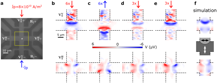
To further evidence the reversible NSOT switching controlled by the current polarity we measure a m wide symmetric cross bar device, shown in Fig. 3a. We start by applying 6 positive pulses along the vertical channel and record the SFOM-MSE map shown in Fig. 3b. After applying 6 negative pulses we obtain the significantly modified image shown in Fig. 3c. When applying again 6 positive pulses, we recover the nearly identical original SFOM-MSE map (cf. Figs. 3b,e).
In Fig. 3f we simulate the SFOM-MSE measurement considering a realistic domain configuration. We compare the measurements shown in Figs. 3b-e with results from self-consistent simulations of the MSE response for the vertical and horizontal bars of a geometrically pinned bubble-shape domain wall in a symmetric cross structure. We consider that due to the higher current density within the bar, domains with their Néel vector parallel to the NSOT driving field enlarge their size to gain the effective Zeeman energyZelezny2014 . The domain wall motion remains restricted by geometric pinning at the cross entrance when moving the domain wall towards the cross center Wunderlich2001 ; Janda2017 . The corresponding self-consistently calculated MSE maps for the vertical bar and the horizontal bar are in good qualitative agreement with our measurements. Details on the simulation as well as a discussion on the small AMR contributions to the thermoelectric signal can be found in the Supplementary Note 1.
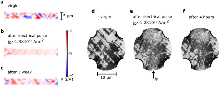
So far we have discussed SFOM-MSE experiments in which electrical pulses of opposite polarity caused reversible Néel vector switching via domain wall displacement in the antiferromagnet with micron-scale domains. When applying stronger pulses of amplitude A/m2, we observe diminishing contrast of the SFOM-MSE signal, as shown in Figs. 4a,b for a m wide bar. We ascribe the vanishing SFOM-MSE contrast to a fragmented multi-domain state of the antiferromagnet with sub-micron feature sizes that are significantly smaller than the extension of the thermal gradient in our SFOM experiment. As a consequence, the net thermoelectric signal from the many domains averages out. Acquiring the full SFOM-MSE image after the pulse takes about 30 minutes. For comparison, we show in Figs. 4d-f XMLD-PEEM measurements on a similar CuMnAs film and with similar pulse amplitudes, taken a few minutes after the pulse (Fig. 4e) and again after 4 hours (Fig. 4f). We see that domains are shattered into a fragmented state with many small sub-micron domains by the current pulse, consistent with the SFOM image in Fig. 4b. The large domains on the left and right side of the horizontal channel remained unaffected since they were not exposed to the current pulse. The domain fragmentation in CuMnAs has been explored in parallel XMLD-PEEM and NV-diamond imaging studies and associated with quenched metastable states which form after pulse-heating the system close to the Néel temperatureWornle2019 ; Kaspar2019 . Systematic electrical readout measurements showed that corresponding resistive switching signals can reach giant-magnetoresistance amplitudes of %, i.e., far exceed the signals associated with NSOT-induced Néel vector reorientations in the unshattered state with domain sizes in the micron-scale or largerWornle2019 ; Kaspar2019 .
Our laboratory SFOM-MSE technique allows for exploring the relaxation of the metastable fragmented states over long time-scales. Remarkably, when re-measuring the SFOM-MSE signal one week after the pulse, we find again large-scale SFOM-MSE pattern which resembles the original pattern measured prior to the applied pulse (cf. Figs. 4 a, c). This observation, consistent with the results of the NV-diamond imagingWornle2019 , hints to the presence of nucleation and pinning centres in the CuMnAs film. On the other hand, we also note that the disappearance of the contrast observed in the SFOM-MSE measurements in short times after the pulse confirm that potential non-magnetic thermoelectric contributions from defects are small compared to the MSE signal from the antiferromagnetic domains.
The interpretation of the SFOM-MSE signal in terms of an actual domain structure may only be justified for sizes larger than the spatial resolution, as highlighted in Fig. 3b-e. However, the feature sizes can be significantly smallerWornle2019 ; Kaspar2019 (see also Figs. 4e,f). In the following we introduce a high resolution method where we can resolve narrow 180∘ antiferromagnetic domain walls in a thin CuMnAs film with uniaxial magnetic anisotropy, and observe polarity dependent 180∘ switching via domain wall displacement.
High resolution imaging of current-induced displacement of 180∘ domain walls
CuMnAs films of thickness nm exhibit a dominant uniaxial magnetic anisotropy component ascribed to the symmetry breaking between the GaP [110] and [10] axes (CuMnAs [100] and [010] axes) at the GaP/CuMnAs interfaceSaidl2017 ; Wadley2015a ; Wang2020 . In such films, narrow 180∘ domain walls separate magnetic domains with reversed Néel vectors as shown, e.g., by XMLD-PEEM measurements on a nm CuMnAs film in Supplementary Note 2.
In the following we present MSE measurements on bar devices patterned from a nm CuMnAs film. (For further discussion of the uniaxial anisotropy in this film as confirmed by our MSE measurements, see Supplementary Note 2.) The detectable MSE-signal in uniaxial films is generated only within the 180∘ antiferromagnetic domain wall since the two neighbouring domains with opposite Néel vectors share the same Seebeck coefficient. In order to image narrow 180∘ domain walls we therefore have to generate a thermal gradient with spatial resolution of the order of the domain wall width. To enhance the spatial resolution we scatter the laser light from a metallic tip, as known from scattering-type SNOM Keilmann2004 . This technique allows us to focus light on a spot size of a few tens of nm, only limited by the tip’s dimensions Mastel2018 , and hence to generate a much sharper thermal gradient as compared to the SFOM method.
In Fig. 5a we illustrate our SNOM-MSE technique. The radiation induced temperature profile underneath the tip is indicated by the red spot. The MSE signal appears as two features of the same intensity but opposite polarity when scanning with the AFM tip over the 180∘ domain wall, since only the variation of the magneto-Seebeck coefficient within the domain wall contributes to the signal. The position where the MSE signal switches sign therefore corresponds to the position of the 180∘ domain wall.
Figure 5b shows a micrograph of a m wide CuMnAs bar device below the cantilever with the AFM tip. The thermoelectric voltage, , generated in the channel is analyzed by a lock-in amplifier at the AFM tip modulation frequency . For tip enhanced focusing we use a scattering-type SNOM operated in the tapping mode. A gold coated Si cantilever with a typical tip diameter below 50 nm oscillates with an amplitude of 80 nm above the sample surface at its mechanical resonance frequency kHz. The continuous wave emission of a quantum cascade laser is focused onto the tip apex which acts as an antenna transmitting a strongly confined near-field to the sample surface. In contrast to our diffraction-limited SFOM method with nm excitation wavelength, we use here a laser emission with mid-infrared wavelength because the longer wavelength couples more efficiently into the AFM tip and the resolution of this near-field method is not diffraction limited.
Figure 5c shows, from left to right, the AFM topography image, the magnitude of the thermoelectric voltage , and its sign , all detected simultaneously during the SNOM-MSE measurement. As evident from the comparison between the SNOM-MSE signal and the AFM topography, the majority of the features appearing in the MSE map do not correlate with defects in the topography. We therefore conclude that also in this uniaxial material the contrast originates dominantly from the antiferromagnetic texture. In order to highlight the position of the 180∘ domain walls, we plot the absolute value of the measured signal alongside with its polarity. We can then identify the 180∘ domain walls as meandering zero-signal lines that surround micron-size antiferromagnetic domains.
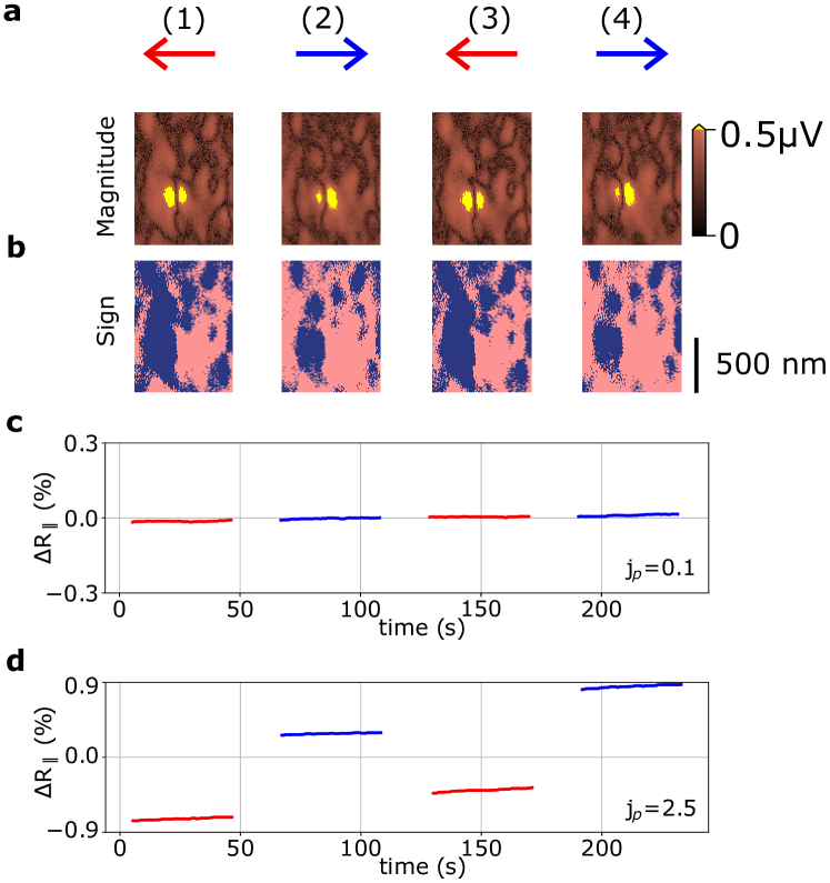
In order to investigate the effect of current-induced NSOT on the 180∘ domain walls we manipulate the magnetic texture by sending current pulses through the bar device, as illustrated in Fig. 6. We apply current pulses of A/m2 with a duration of 1 ms and with alternating polarity in order to illustrate the reversible switching; the current direction is shown by the red and blue arrows. Note that the onset current amplitude for switching in the 20 nm CuMnAs film is higher than in the above switching experiments in the 45 nm film. We do not attribute it to the difference of intrinsic properties of the two films. It results from the heat-assisted nature of switchingOlejnik2018 ; Kaspar2019 and from an interplay of device geometry and heat dissipation during the writing pulse. For ultrashort pulses (with lengths in the ns-scale or smaller), the temperature increase of the CuMnAs device is determined by the energy density delivered by the pulse. Hence, the onset current density for switching does not depend on the dimensions of the CuMnAs deviceOlejnik2018 . For longer pulses, including those used in the present work, the effect of heat dissipation from the device during the pulse becomes important. Consequently, the current density required to achieve the same switching temperature increases with decreasing film thickness.
In Figs. 6a,b we plot a zoom of the measured and after applying a train of 22 current pulses before applying the train of current pulses again with opposite polarity. We found that depending on the polarity of the applied pulses, the antiferromagnetic domains change their size by reversibly displacing domain walls, consistent with the NSOT driven antiferromagnetic domain wall motion Gomonay2016 ; Otxoa2020 . The corresponding resistance changes are plotted in Figs. 6c,d. After applying pulses of amplitude A/m2, we observe in Fig. 6d bistable changes of the bar resistance of the order of . In comparison, no changes are observed for A/m2, as shown in Fig. 6c. We attribute the resistance variations to magnetic scattering on the domain walls; the AMR contributions from the antiferromagnetic domains can be excluded in the uniaxial film. More details on the switching as a function of the polarity, number and amplitude of the current pulses by means of principal components analysis can be found in the Supplementary Note 3.
Conclusions
We have introduced a laboratory method for imaging antiferromagnetic domain structure by mapping the local magneto-Seebeck effect using a far-field or near-field optical scanning approach. In uniaxial CuMnAs, we identify narrow 180∘ domain walls of sub-micron width and their pulse induced displacements. These reversible, polarity-dependent modifications of the antiferromagnetic domain maps are consistent with the current-induced NSOT switching mechanism. We link the imaged domain changes to resistive switching signals which we attribute to scattering on the 180∘ domain walls. In biaxial CuMnAs, we confirm large micron size domains and their Current-pulse-induced modifications. We conclude that AMR from the 90∘ Néel vector reorientation in the antiferromagnetic domains can explain only part of the measured resistance variations. We suggest that magnetic scattering on domain walls gives a strong additional contribution to the observed resistive switching. Apart from the polarity dependent NSOT reorientation of the Néel vector at lower pulse amplitudes we also confirm shattering into fragmented metastable multi-domain states with sub-micron feature sizes after applying larger amplitude pulses, and the subsequent relaxation towards the pre-pulsed state of the antiferromagnet.
References
- (1) Jungwirth, T., Marti, X., Wadley, P. & Wunderlich, J. Antiferromagnetic spintronics. Nature Nanotechnology 11, 231–241 (2016). eprint 1606.04284.
- (2) Baltz, V. et al. Antiferromagnetic spintronics. Reviews of Modern Physics 90, 015005 (2018). URL https://doi.org/10.1103/RevModPhys.90.015005.
- (3) Železný, J., Wadley, P., Olejník, K., Hoffmann, A. & Ohno, H. Spin transport and spin torque in antiferromagnetic devices. Nature Physics 14, 220–228 (2018).
- (4) Gomonay, O., Baltz, V., Brataas, A. & Tserkovnyak, Y. Antiferromagnetic spin textures and dynamics. Nature Physics 14, 213–216 (2018). URL http://dx.doi.org/10.1038/s41567-018-0049-4.
- (5) Němec, P., Fiebig, M., Kampfrath, T. & Kimel, A. V. Antiferromagnetic opto-spintronics. Nature Physics 14, 229–241 (2018). URL http://dx.doi.org/10.1038/s41567-018-0051-x.
- (6) Šmejkal, L. & Jungwirth, T. Symmetry and topology in antiferromagnetic spintronics. In Zang, J., Cros, V. & Hoffmann, A. (eds.) Topology in magnetism, 267–298 (Springer International Publishing, 2018). URL http://arxiv.org/abs/1804.05628.
- (7) Shick, A. B., Khmelevskyi, S., Mryasov, O. N., Wunderlich, J. & Jungwirth, T. Spin-orbit coupling induced anisotropy effects in bimetallic antiferromagnets: A route towards antiferromagnetic spintronics. Physical Review B 81, 212409 (2010). eprint 1002.2151.
- (8) Železný, J. et al. Relativistic néel-order fields induced by electrical current in antiferromagnets. Physical Review Letters 113, 157201 (2014). eprint 1410.8296.
- (9) Park, B. G. et al. A spin-valve-like magnetoresistance of an antiferromagnet-based tunnel junction. Nature Materials 10, 347–351 (2011).
- (10) Marti, X. et al. Room-temperature antiferromagnetic memory resistor. Nature Materials 13, 367–374 (2014). URL http://www.nature.com/articles/nmat3861. eprint 0402594v3.
- (11) Wadley, P. et al. Electrical switching of an antiferromagnet. Science 351, 587–590 (2016). eprint 1503.03765.
- (12) Godinho, J. et al. Electrically induced and detected Néel vector reversal in a collinear antiferromagnet. Nature Communications 9, 4686 (2018). URL http://arxiv.org/abs/1806.02795. eprint 1806.02795.
- (13) Grzybowski, M. J. et al. Imaging Current-Induced Switching of Antiferromagnetic Domains in CuMnAs. Physical Review Letters 118, 057701 (2017). eprint 1607.08478.
- (14) Wadley, P. et al. Current polarity-dependent manipulation of antiferromagnetic domains. Nature Nanotechnology 13, 362–365 (2018). URL http://www.nature.com/articles/s41565-018-0079-1. eprint arXiv:1711.05146.
- (15) Moriyama, T., Oda, K., Ohkochi, T., Kimata, M. & Ono, T. Spin torque control of antiferromagnetic moments in NiO. Scientific Reports 8, 14167 (2018). URL http://arxiv.org/abs/1708.07682http://www.nature.com/articles/s41598-018-32508-w. eprint 1708.07682.
- (16) Reichlova, H. et al. Imaging and writing magnetic domains in the non-collinear antiferromagnet Mn3Sn. Nature Communications 10, 5459 (2019). URL http://dx.doi.org/10.1038/s41467-019-13391-zhttp://www.nature.com/articles/s41467-019-13391-z. eprint 1905.13504.
- (17) Gray, I. et al. Spin Seebeck Imaging of Spin-Torque Switching in Antiferromagnetic Pt/NiO Heterostructures. Physical Review X 9, 041016 (2019). URL https://doi.org/10.1103/PhysRevX.9.041016. eprint 1810.03997.
- (18) Bodnar, S. Y. et al. Imaging of current induced néel vector switching in antiferromagnetic . Phys. Rev. B 99, 140409 (2019). URL https://link.aps.org/doi/10.1103/PhysRevB.99.140409.
- (19) Baldrati, L. et al. Mechanism of Néel Order Switching in Antiferromagnetic Thin Films Revealed by Magnetotransport and Direct Imaging. Physical Review Letters 123, 177201 (2019). URL http://arxiv.org/abs/1810.11326https://link.aps.org/doi/10.1103/PhysRevLett.123.177201. eprint 1810.11326.
- (20) Wörnle, M. S. et al. Current-induced fragmentation of antiferromagnetic domains (2019). URL http://arxiv.org/abs/1912.05287. eprint 1912.05287.
- (21) Kašpar, Z. et al. High resistive unipolar-electrical and fs-optical switching in a single-layer antiferromagnetic memory 1–22 (2019). URL http://arxiv.org/abs/1909.09071. eprint 1909.09071.
- (22) Chiang, C. C., Huang, S. Y., Qu, D., Wu, P. H. & Chien, C. L. Absence of Evidence of Electrical Switching of the Antiferromagnetic Néel Vector. Physical Review Letters 123, 227203 (2019). URL https://link.aps.org/doi/10.1103/PhysRevLett.123.227203.
- (23) Zink, B. The Heat in Antiferromagnetic Switching. Physics 12, 134 (2019).
- (24) Zhang, P., Finley, J., Safi, T. & Liu, L. Quantitative Study on Current-Induced Effect in an Antiferromagnet Insulator/Pt Bilayer Film. Physical Review Letters 123, 247206 (2019). URL http://arxiv.org/abs/1907.00314. eprint 1907.00314.
- (25) Cheng, Y., Yu, S., Zhu, M., Hwang, J. & Yang, F. Electrical Switching of Tristate Antiferromagnetic Néel Order in alpha Fe2O3 Epitaxial Films. Physical Review Letters 124, 027202 (2020). URL http://arxiv.org/abs/1906.04694{%}0Ahttps://link.aps.org/doi/10.1103/PhysRevLett.124.027202. eprint 1906.04694.
- (26) Churikova, A. et al. Non-magnetic origin of spin Hall magnetoresistance-like signals in Pt films and epitaxial NiO/Pt bilayers. Applied Physics Letters 116, 022410 (2020). URL http://aip.scitation.org/doi/10.1063/1.5134814.
- (27) Scholl, A. Observation of Antiferromagnetic Domains in Epitaxial Thin Films. Science 287, 1014–1016 (2000). URL https://www.sciencemag.org/lookup/doi/10.1126/science.287.5455.1014.
- (28) Degen, C. L. Scanning magnetic field microscope with a diamond single-spin sensor. Applied Physics Letters 92, 243111 (2008).
- (29) Balasubramanian, G. et al. Nanoscale imaging magnetometry with diamond spins under ambient conditions. Nature 455, 648–651 (2008). URL http://www.nature.com/articles/nature07278.
- (30) Kosub, T. et al. Purely antiferromagnetic magnetoelectric random access memory. Nature Communications 8, 13985 (2017). URL http://www.nature.com/articles/ncomms13985. eprint 1611.07027.
- (31) Gross, I. et al. Skyrmion morphology in ultrathin magnetic films. Physical Review Materials 2, 024406 (2018). URL http://arxiv.org/abs/1709.06027{%}0Ahttp://dx.doi.org/10.1103/PhysRevMaterials.2.024406https://link.aps.org/doi/10.1103/PhysRevMaterials.2.024406. eprint 1709.06027.
- (32) Wadley, P. et al. Tetragonal phase of epitaxial room-temperature antiferromagnet CuMnAs. Nature Communications 4, 2322 (2013). eprint 1402.3624.
- (33) Wadley, P. et al. Antiferromagnetic structure in tetragonal CuMnAs thin films. Scientific Reports 5, 17079 (2015).
- (34) Weiler, M. et al. Local charge and spin currents in magnetothermal landscapes. Physical Review Letters 108, 106602 (2012). eprint arXiv:1110.3981.
- (35) Pfitzner, E. et al. Near-field magneto-caloritronic nanoscopy on ferromagnetic nanostructures. AIP Advances 8, 125329 (2018).
- (36) Woessner, A. et al. Near-field photocurrent nanoscopy on bare and encapsulated graphene. Nature Communications 7, 10783 (2016). eprint 1508.07864.
- (37) Lundeberg, M. B. et al. Thermoelectric detection and imaging of propagating graphene plasmons. Nature Materials 16, 204–207 (2017).
- (38) Krzysteczko, P., Hu, X., Liebing, N., Sievers, S. & Schumacher, H. W. Domain wall magneto-Seebeck effect. Physical Review B 92, 1–5 (2015). eprint 1412.8289.
- (39) Wang, M. et al. Spin flop and crystalline anisotropic magnetoresistance in CuMnAs. Physical Review B 101, 094429 (2020). URL http://arxiv.org/abs/1911.12381https://link.aps.org/doi/10.1103/PhysRevB.101.094429. eprint 1911.12381.
- (40) Wunderlich, J. et al. Influence of geometry on domain wall propagation in a mesoscopic wire. IEEE Trans. Mag. 37, 2104–2107 (2001).
- (41) Janda, T. et al. Inertial displacement of a domain wall excited by ultra-short circularly polarized laser pulses. Nature Communications 8, 15226 (2017). URL http://www.nature.com/articles/ncomms15226.
- (42) John Robert Schrieffer - Theory of Superconductivity (1999, Westview Press).
- (43) Saidl, V. et al. Optical determination of the Néel vector in a CuMnAs thin-film antiferromagnet. Nature Photonics 11, 91–96 (2017). eprint 1608.01941.
- (44) Keilmann, F. & Hillenbrand, R. Near-field microscopy by elastic light scattering from a tip. Philosophical Transactions of the Royal Society of London. Series A: Mathematical, Physical and Engineering Sciences 362, 787–805 (2004). URL https://royalsocietypublishing.org/doi/10.1098/rsta.2003.1347.
- (45) Mastel, S. et al. Understanding the Image Contrast of Material Boundaries in IR Nanoscopy Reaching 5 nm Spatial Resolution. ACS Photonics 5, 3372–3378 (2018).
- (46) Olejník, K. et al. Terahertz electrical writing speed in an antiferromagnetic memory. Science Advances 4, eaar3566 (2018). URL http://advances.sciencemag.org/lookup/doi/10.1126/sciadv.aar3566. eprint 1711.08444.
- (47) Gomonay, O., Jungwirth, T. & Sinova, J. High Antiferromagnetic Domain Wall Velocity Induced by Néel Spin-Orbit Torques. Physical Review Letters 117, 017202 (2016). eprint 1602.06766.
- (48) Otxoa, R. M., Roy, P. E., Rama-Eiroa, R., Giuslienko, K. Y. & Wunderlich, J. Walker-like domain wall breakdown in layered antiferromagnets driven by staggered spin-orbit fields (2020). URL http://arxiv.org/abs/2002.03332. eprint 2002.03332.
Acknowledgments B.K., A.H and G.U. acknowledge funding from the EMPIR programme (JRP ADVENT) co-financed by the Participating States and from the European Union s Horizon 2020 research and innovation programme. E.P. and J.H. acknowledge funding from the DFG-project HE 2063/5-1. T.Ja., J.G.,ZT.S., H.R.,V.N., K.O., J.W. and T.Ju. acknowledge funding from Ministry of Education of the Czech Republic Grant No. LM2018110 and LNSM-LNSpin, of the Czech Science Foundation Grant No. 19-28375X, and for the EU FET Open RIA Grant No. 766566. J.G., V.N., K.O., and J.W. acknowledges funding from the ERC Synergy grant no. 610115. We acknowledge Diamond Light Source for time on Beamline I06 under proposal nos. SI16376 and SI20793.
Author contributions
T.Ja., P.N., and J.W. planned and prepared the SFOM-MSE measurements, which T.Ja. and J.G. carried out. G.U., E.P. , A.H., and B.K. planned and prepared the SNOM-MSE measurements, which J.W., G.U., E.P., A.H., J.G., H.R., T.M., and B.K. carried out. J.G., H.R., J.W., and K.O. planned and performed the electrical pulsing experiments. S.R., O.J.A, J.S.C., P.W., K.W.E., S.S.D., F.M. planned and performed the XMLD-PEEM measurements. T.O. performed the simulations. V.N., R.P.C., and P.W. grew and characterized the CuMnAs films. Z.S. designed and fabricated the devices. J.W., B.K., J.G., T.Ja., T.O., T.M., E.P., and T.Ju. wrote the paper . All authors discussed the results and contributed to the manuscript. B.K. and J.W. conceived and planned the study.
Additional information Corresponding authors correspondence to T. Janda, J. Godinho, B. Kaestner, and J. Wunderlich.
Methods
Sample fabrication For patterning our samples we used standard electron beam lithography on an PMMA resist film after cleaning the surface of our CuMnAs wafers with acetone. After removing the Al/AlOx capping layer using diluted TMAH developer the individual devices were defined by etching insulating trenches using a mixture of H2SO4, C4H6O6, H2O2, and DI H2O. Bonding contacts were made using a lift-off process following the Cr(3 nm)Au(80 nm) evaporation.
SFOM-MSE technique The laser beam emited by a Ti:Sapphire continuous-wave (cw) laser (Spectra Physics, model 3900S) tuned to a wavelength of nm is focused into a spot-size of m full width at half maximum (FWHM) by an objective lens (Mitutoyo Plan Apo 20). The data in Fig. 1 was measured with a laser power of mW and the data in Figs. 2–4 with a power of mW. Since the MSE signal is linear in the laser power (as confirmed by a test measurement, not shown here) the only effect of a larger laser power is a correspondingly larger MSE voltage and a higher signal to noise ratio. Scanning of the laser spot across the sample surface is achieved by moving the objective lens with a 3D piezo-positioner (Newport, NPXYZ100SG-D). The laser beam is modulated at a frequency of kHz by an optical chopper and from the measured and amplified MSE voltage the signal component at the chopper-frequency is extracted by a lock-in amplifier.
SNOM-MSE technique The emission of a quantum cascade laser (QCL, 28 mW at m, MIRcat, Daylight Solutions Inc., CA, USA) was focussed onto the metallic tip apex of the metal-coated Si cantilever (neaspec nano-FTIR Scanning Probes). Focussing and scanning of the tip was performed using a commercial scattering-type scanning nearfield optical microscopy instrument (Neasnom, by Neaspec GmbH). The tip-mediated electric response of the sample was amplified by low-noise voltage preamplifier (Stanford Research SR 560, gain ), and further demodulated at the tip-modulation frequency and its higher harmonics with the lock-in amplifier of the Neasnom instrument. Both, amplitude and phase, were recorded while scanning the sample surface.
Figure Captions
Figure 1 Comparison between laboratory optical and synchrotron x-ray images of the domain structure in bar-shaped patterned antiferromagnetic CuMnAs. a, Schematics of the measurement setup for the laboratory SFOM-MSE technique (top panel). A focused laser beam creates a local thermal gradient. When scanned over an antiferromagnetic (purple and grey arrows) texture, the in-plane components of the thermal gradient generate a voltage across the bar due to the MSE (bottom panel). b, Optical micrograph of four 50 m long and 5 m wide bars patterned from a 45 nm thick CuMnAs epilayer along [100], [10], [110], and [010] crystallographic axes of CuMnAs. c, Comparison between SFOM-MSE and XMLD-PEEM measurements in the four microbars. Antiferromagnetic domain structure is observed by XMLD-PEEM for X-ray polarization crystal axis. The single- and double-headed arrows in c indicate the in-plane projection of the X-ray propagation vector and the X-ray polarization vector, respectively. The light (dark) contrast corresponds to antiferromagnetic domains with the Néel vector oriented perpendicular (parallel) to the X-ray polarization.
Figure 2 Current-pulse-induced modification of the domain structure detected by MSE scans and compared to AMR measurements. a, SEM micrograph of a 5m wide cross bar patterned from a 45 nm thick CuMnAs epilayer. The MSE scans have been performed within the the area of m2, indicated by the yellow dashed line. b, MSE signal measured along the vertical bar after 7 trains of positive pulses (left) followed by 10 trains of negative pulses (right). Each train of pulses contains 6 individual pulses c, MSE signal simultaneously measured along the horizontal bar. d, Corresponding variation of the magnetoresistance measured in a 4-point geometry along the vertical bar. Red (blue) data points correspond to resistance measurements after current pulses of positive (negative) polarity with A/m2 and ms.
Figure 3 Reproducibility of antiferromagnetic texture after pulsing with alternating polarity a, Optical micrograph of a m wide cross bar, showing the measurement contacts geometry used. b - e Sequence of MSE maps of the vertical thermoelectric voltage and horizontal thermoelectric voltage measured simultaneously for alternating pulses. The MSE scans were performed within the area highlighted by the yellow dashed line in a. f, Simulated MSE maps of (upper graph) and (lower graph) for a domain configuration of a geometrically pinned domain wall (middle schematics) by taking into account the experimental conditions of a focused laser spot with Gaussian profile of m FWHM, mW laser power and by assuming a magneto-Seebeck coefficient of V/K.
Figure 4 Shattering of magnetic domains after an electrical pulse. a, SFOM-MSE scan of a m wide bar device prior to any electrical pulse. b, After a pulse with a current density of A/m2 the contrast is lost with the main features absent. The loss of contrast is ascribed to the shattering of the magnetic domains into smaller domains, which become significantly smaller than the spatial resolution of the SFOM-MSE. Hence, the total SFOM-MSE signal over many domain walls averages nearly to zero. c, The SFOM-MSE signal one week after the electrical pulse, where a similar pattern of large domains has reappeared and is resembling the initial state in a. d, XMLD-PEEM measurements prior the pulse, e, just after the pulse with a current density of A/m2 e, and f, 4 hours after the pulse.
Figure 5 SNOM-MSE scan of a bar device patterned from a uniaxial CuMnAs layer. a, Schematics of the SNOM-MSE setup. The thermal gradient is created when a metal-coated AFM tip interacts with an infra-red laser, inducing an optical near-field at the apex of the tip. A domain wall appears in the MSE maps as two features of opposite sign together, as illustrated in the bottom panel. b, Micrograph of the scanned bar-device, where the AFM tip is also visible. c, From left to right: topography map, magnitude of the MSE signal and its sign.
Figure 6 Reversible switching measured in SNOM-MSE. a, Maps of the magnitude of the MSE signal, , after applying current pulses of amplitude A/m2 in opposite directions indicated by the red and blue arrow on top. b, Maps of the corresponding values. c,d, Resistance variations associated with the corresponding switching states for low and high current densities. Current density values shown are in A/m2.