Threedimensional Alternating-Phase Focusing for Dielectric-Laser Electron Accelerators
Abstract
The concept of dielectric-laser acceleration (DLA) provides the highest gradients among breakdown-limited (nonplasma) particle accelerators and thus the potential of miniaturization. The implementation of a fully scalable electron accelerator on a microchip by twodimensional alternating phase focusing (APF), which relies on homogeneous laser fields and external magnetic focusing in the third direction, was recently proposed. In this Letter, we generalize the APF for DLA scheme to 3D, such that stable beam transport and acceleration is attained without any external equipment, while the structures can still be fabricated by entirely twodimensional lithographic techniques. In the new scheme, we obtain significantly higher accelerating gradients at given incident laser field by additionally exploiting the new horizontal edge. This enables ultra-low injection energies of about 2.5 keV () and bulky high voltage equipment as used in previous DLA experiments can be omitted. DLAs have applications in ultrafast time-resolved electron microscopy and -diffraction. Our findings are crucial for the miniaturization of the entire setup and pave the way towards integration of DLAs in optical fiber driven endoscopes, e.g., for medical purposes.
Dielectric Laser Acceleration (DLA) was already proposed in 1962 [1, 2], however, first experiments came 50 years later [3, 4] by means of femtosecond laser pulses and lithographic nanofabrication. Recent advances in ultrashort laser pulses have enabled demonstrations of damage-threshold and self phase-modulation limited record gradients approaching the GeV/m milestone for relativistic electrons [5, 6]. At subrelativistic energies, driven by a table-top electrostatic pre-accelerator, gradients of 133 MeV/m [7] and 370 MeV/m [8] were achieved in silicon pillar structures. In order to create a functioning accelerator out of these impressive gradients, the interaction length needs to be increased while maintaining a stable 6D phase space confinement. First approaches to beam dynamics in grating linacs were already made in the 1980’ [9, 10, 11]. In 2012, Naranjo et al. [12] showed that the nonsynchronous spatial (sub-) harmonics can provide a ponderomotive focusing force, which was later turned into an accelerator design for medium energy [13]. Another approach starts from showing that a periodic grating provides phase dependent forces which can be concentrated in one kick per grating cell [14]. Per Panofsky-Wenzel theorem [15], this threedimensional kick is irrotational, and can thus be modeled as a (time-dependent) potential in the Hamiltonian. Removing the time-dependence is achieved by lattice integration of the linearized fields according to the Courant-Snyder (CS) theory [16]. An accelerator lattice design providing stable motion in the longitudinal and one transverse direction is obtained by an Alternating Phase Focusing (APF) arrangement of grating segments treated as thick lenses [17]. Full scalability of the APF-DLA is achieved by using a pulse-front-tilted (PFT) laser [18, 19, 20] or an on-chip photonic waveguide system [21], which in principle allows to work with arbitrary short pulses.
The equivalent magnetic focusing strength of an individual APF segment was predicted [17] and experimentally demonstrated to be in the MT/m range [22]. Moreover, the energy modulation of a subrelativistic DLA can also be turned into ballistic bunching [23, 24, 25], however, the hereby created energy spread is too large to inject into a scalable APF-DLA accelerator. A proposed APF-based segmented buncher [17] solves this problem and is currently being experimentally tested. Another ongoing experiment is the demonstration of a periodically segmented APF transport channel [26], which is however limited in length by the Rayleigh range of the electron beam in the invariant direction. In [17], we proposed to overcome this limit by installing an external quadrupole magnet which constantly focuses the beam in the vertical direction. A major challenge in the experimental realization of a fully scalable APF-DLA is the alignment of this external magnet and the sufficient homogeneity of the laser fields in the invariant vertical direction of the structure.
In this Letter, we generalize the APF-based confinement to both transverse directions. This enables to completely eliminate external focusing devices in scalable DLAs of arbitrary length. Moreover, since the additional dimension provides an additional edge, the accelerating near-field is increased, allowing to push for lower injection energy at given aperture. Previously reported minimal injection energies of keV [27] required using higher harmonics (in [27] the 5th) and confinement was not attained. Here, we intend to stay at the first harmonic since it provides the slowest drop-off from the grating surface and thus the highest center gradient. We show, that injection energies of 16.75 keV and 2.5 keV are attainable at laser wavelengths of 2 m and 6 m, respectively. Thus, bulky high voltage feedthroughs in the experimental chambers can be entirely omitted.
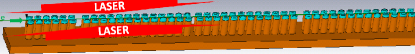

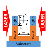


The 3D APF-based DLA can still be fabricated by 2D lithographic techniques. The key idea is to work with two materials, exhibiting an as high as possible refractive index contrast, see Fig. 1. Such technology is already commercially available in nano-electronics and -photonics, e.g. as Silicon-on-Insulator (SOI) wafers [28] and has been used to demonstrate a waveguide driven DLA recently [29]. The refractive indices at 2m are [30] and , respectively. At first, we make the approximation of , which will be later refined. In other words, the oxide serves as just a building brick to construct 3D silicon structures by 2D lithography, where the layer thickness and the pillar semi-axis radii can attain single digit nanometer precisions.
To model the electromagnetic fields in the (quasi-) periodic structures, we first look at the Helmholtz wave equation, in temporal frequency domain and Fourier series expanded in the longitudinal direction (see [14]),
| (1) |
where is the transverse Laplacian, is the longitudinal wave number of the synchronous mode to an electron traveling at speed and . Equation 1 is valid only in the vacuum of the beam channel. In contrast to conventional metallic accelerators, this creates the problem that boundary conditions, necessary to solve Eq. 1, are not available. We can however determine the dispersion relation from Eq. 1 by , , and as
| (2) |
which is plotted in Fig. 2. Instead of solving Eq. 1, we only need to determine and one transverse wave number, which can be done numerically (we use CST [31] as described in [14]) for each individual grating cell with periodic boundary conditions in -direction. The transverse dependence of can then be written analytically as
| (3) |
which is numerically confirmed within 5% in the channel and plotted in Fig. 1 over a slightly larger range. The assumption that the oxide can be neglected is crosschecked in Fig. 3, where , , and are compared for a free floating simplified pillar, a full pillar with the origin centered in , and a full pillar with the origin (i.e. the expansion point) shifted by 10 nm towards the substrate. Since the curves agree to sufficient accuracy, we will continue with the simplified pillars for brevity.
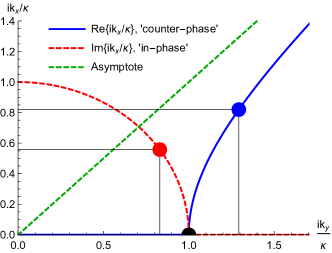
For the laser traveling in -direction and polarized in -direction, is always a purely real number. However, can either be purely real or purely imaginary, see Fig. 2. We will refer to these cases as in-phase and counter-phase scheme, indicating whether or not both transverse planes are simultaneously focused.
With no loss of generality, we continue with the counter-phase scheme only, since the structures are straightforward to fabricate on SOI wafers. The dependence of the wavenumbers as well as on the height of a free floating pillar is plotted in Fig. 4. The dashed lines correspond to the 2D () case as introduced in [17] (black dot in Fig. 2). The oscillation of is due to eigenmodes arising in the -direction. Subsequently, the 2D case holds only for discrete values of . These roots (and the corresponding maxima) of are not robust with respect to perturbations such as attaching the pillar to the oxide or to the substrate. Robust counter-phase focusing behavior is however found below the first root of , where also a 40% enhancement of due to the finite height appears. A reasonable thickness of m (commercially available [28]) is chosen, slightly below this first maximum. A numerical parameter scan over using CST [31] provides the results as depicted in Fig. 3, where the entire curve is produced by an identical pillar design and only the cell length is swept in order to always fulfill the Wideroe condition . Keeping the same pillar dimensions over a range of requires compensating the phase drift, which is achieved by shifting the pillar center off the cell center by [32]. This allows to use only about 4 or 5 different pillar designs to cover the entire range from extremely low energy to relativistic () beams, which consists of in the order of pillar pairs.

With the above knowledge of the electromagnetic field, we proceed to the Hamiltonian , where is the momentum deviation from the reference particle and is the electron rest mass. The time-dependent potential reads generally (same procedure as in [17]) as
| (4) |
where is the (negative) electron charge, is the relative longitudinal coordinate w.r.t. the laser phase, and is the synchronous phase at which the reference particle gains energy according to the design acceleration ramp. Tracking with the nonlinear kicks according to Eq. 4 can be performed using DLAtrack6D [14]. Expanding Eq. 4 to second order, Hamilton’s equations provide the Hill’s equations
| (5a) | ||||
| (5b) | ||||
| (5c) | ||||
where . Due to the absence of first order terms in , the linearized motion is decoupled.


The focusing functions are
| (6a) | ||||
| (6b) | ||||
| (6c) | ||||
and fulfill according to Eq. 2, which reflects Earnshaw’s theorem [33]. Note that is the same as in the 2D scheme [17] and the and planes are alternatingly focused by switching using fractional period drifts. The numerical value of is however different from the 2D case and thus all three frequencies (and subsequently phase advances) are disparate.
This general description of the motion is now turned into a functioning accelerator that provides 3D particle confinement by individual CS lattice integration [16] in each plane . As in [17], the lattice functions in Eqs. 6 are converted to CS-functions (also called Twiss parameters) by solving the Twiss map eigenvector problem for the initial values and subsequently mapping them to any other position. An example of a pure transport structure, which is strictly periodic, is shown in Fig. 5. The parameter choice can be understood as a multi-objective optimization to find the minimum for the maxima of the functions in all three dimensions, with a common APF cell length and a common incident laser field strength. A suitable choice on the resulting Pareto-front is the minimum of the arithmetic average of the three maxima of the functions.
These individual cells are now combined to a full accelerator on a chip. Initially we pick the injection energy and the synchronous phase, which is a compromise between desired acceleration gradient and required longitudinal focusing strength. The laser field strength is picked as slightly below the damage threshold fluence for a (curved-tilted) 100 fs pulse [32]. A laser amplitude of 500 MV/m from each side and a synchronous phase of off-crest are chosen, leading to an average gradient of 500 MeV/m 73 MeV/m, where is the normalized synchronous mode coefficient. The acceleration ramp is determined by adding up the exact energy gains for each DLA cell .
For a continuum of velocities , the maps of each segment in each plane of the lattice are determined successively by solving eigenvalue problems for assumed periodic segments. The length of each cell is taken as the arithmetic average of the minima of the maxima as indicated in Fig. 5. Usually, a lattice obtained by simple matrix mapping of will exhibit growing -functions, due to cummulation of the small mismatch between two APF cells. Smooth and slowly growing -functions, such that the envelopes are non-growing, are obtained by manual correction of the segment lengths. Note that a slight growth of is tolerable, since the emittance decreases by adiabatic damping according to , where the normalized emittance is an invariant of the linearized motion.

The resulting envelopes for a design for 16.75 keV () to 70 keV () are plotted in Fig. 6. After a full 3D field simulation [31], the complex field result along the channel is plotted below. Windowing this global field for each DLA cell allows a comparison between the in the entire accelerator to the individual initially computed under periodic boundary conditions (cf. Fig. 3). As visible, the phase drift compensation keeps constant, but at the -jumps a Gibbs phenonmenon is visible. Eventually this will have a detrimental effect on emittance preservation. The injection parameters were chosen as Gaussian distributions with geometric emittances pm, pm, and bunch length 5 nm with matched energy spread. These values are at the clipping point, where strong beam losses start to occur. The throughput and energy spread is shown in Fig. 7 for one-kick-per-cell vs. 3D full field tracking. Similar results for 2.5 keV () to 16.75 keV () using m are discussed in the Supplemental Material [32] and in principle, one could even start at a few eV only, by using a Terahertz driver. However, lowering the injection energy poses a challenge to the robustness. Structure bandwidth, fabrication tolerances, and injection energy mismatch have to be controlled more precise. Normalized emittances in the single digit picometer range are available [34, 35], however, after the electrostatic pre-accelerator mostly higher values are reported (e.g. [36]). This is due to nonlinear aberrations in the electrostatic lensing system. Our findings ease this problem significantly, since aberrations scale with the overall size of the system, which can be significantly reduced at lower injection energy.
As confirmed by full 3D simulation, the 3D-APF-DLA scheme on SOI wafers is ready for experimental testing. Beyond the double sided lateral laser illumination one might also consider single beam top illumination or even pinched pure silicon pillars [37]. More detailed theoretical studies are required to assess the effects of nonlinear and coupled particle-amplitude-dependent tune spreads, e.g., with the extended DLAtrack6D [38].
U.N. would like to thank Peyman Yousefi, Payton Broaddus, and Olav Solgaard for the discussions on SOI wafer processing. This work is funded by the Gordon and Betty Moore Foundation under Grant No. GBMF4744 (ACHIP).
References
- Lohmann [1962] A. Lohmann, Electron Acceleration by Light Waves, IBM Technical Note 5, 169 (1962).
- Shimoda [1962] K. Shimoda, Proposal for an Electron Accelerator Using an Optical Maser, Applied Optics 1, 33 (1962).
- Breuer and Hommelhoff [2013] J. Breuer and P. Hommelhoff, Dielectric laser acceleration of 28 keV electrons with the inverse Smith-Purcell effect, Nuclear Instruments and Methods in Physics Research, Section A: Accelerators, Spectrometers, Detectors and Associated Equipment 740, 114 (2013).
- Peralta et al. [2013] E. A. Peralta, K. Soong, R. J. England, E. R. Colby, Z. Wu, B. Montazeri, C. McGuinness, J. McNeur, K. J. Leedle, D. Walz, E. B. Sozer, B. Cowan, B. Schwartz, G. Travish, and R. L. Byer, Demonstration of electron acceleration in a laser-driven dielectric microstructure., Nature 503, 91 (2013).
- Wootton et al. [2016] K. P. Wootton, Z. Wu, B. M. Cowan, A. Hanuka, I. V. Makasyuk, E. A. Peralta, K. Soong, R. L. Byer, and R. J. England, Demonstration of acceleration of relativistic electrons at a dielectric microstructure using femtosecond laser pulses, Opt. Lett. 41, 2696 (2016).
- Cesar et al. [2018a] D. Cesar, S. Custodio, J. Maxson, P. Musumeci, X. Shen, E. Threlkeld, R. J. England, A. Hanuka, I. V. Makasyuk, E. A. Peralta, K. P. Wootton, and Z. Wu, High-field nonlinear optical response and phase control in a dielectric laser accelerator, Communications Physics 1, 1 (2018a).
- Yousefi et al. [2018] P. Yousefi, J. McNeur, M. Kozák, U. Niedermayer, F. Gannott, O. Lohse, O. Boine-Frankenheim, and P. Hommelhoff, Silicon dual pillar structure with a distributed Bragg reflector for dielectric laser accelerators: Design and fabrication, Nuclear Instruments and Methods in Physics Research, Section A: Accelerators, Spectrometers, Detectors and Associated Equipment 909, 221 (2018).
- Leedle et al. [2015] K. J. Leedle, R. Fabian Pease, R. L. Byer, and J. S. Harris, Laser acceleration and deflection of 963 keV electrons with a silicon dielectric structure, Optica 2, 158 (2015).
- Palmer [1980] R. B. Palmer, A Laser Driven Grating Linac, Particle Accelerators 11, 375 (1980).
- Kim and Kroll [1982] K. Kim and N. Kroll, Some Effects of the Transverse-Stability Reqirement on the Design of a Grating Linac, LBL-14378 (1982).
- Pickup [1985] M. Pickup, A Grating Linac at Microwave Frequencies, CLNS-85/655 (1985).
- Naranjo et al. [2012] B. Naranjo, A. Valloni, S. Putterman, and J. B. Rosenzweig, Stable charged-particle acceleration and focusing in a laser accelerator using spatial harmonics, Physical Review Letters 109, 164803 (2012).
- Cesar et al. [2019] D. Cesar, P. Musumeci, and J. England, AII Optical control of beam dynamics in a DLA, 2018 IEEE Advanced Accelerator Concepts Workshop, ACC 2018 - Proceedings 10.1109/AAC.2018.8659380 (2019).
- Niedermayer et al. [2017a] U. Niedermayer, T. Egenolf, and O. Boine-Frankenheim, Beam Dynamics Analysis of Dielectric Laser Acceleration using a Fast 6D Tracking Scheme, Phys. Rev. AB 20, 111302 (2017a).
- Panofsky and Wenzel [1956] W. K. H. Panofsky and W. A. Wenzel, Some Considerations Concerning the Transverse Deflection of Charged Particles in Radio-Frequency Fields, Review of Scientific Instruments 27, 31 (1956).
- Courant and Snyder [1958] E. Courant and H. Snyder, Theory of the alternating-gradient synchrotron, Annals of Physics 3, 1 (1958).
- Niedermayer et al. [2018] U. Niedermayer, T. Egenolf, O. Boine-Frankenheim, and P. Hommelhoff, Alternating-Phase Focusing for Dielectric-Laser Acceleration, Physical Review Letters 121, 214801 (2018).
- Wei et al. [2017] Y. Wei, M. Ibison, G. Xia, J. D. A. Smith, and C. P. Welsch, Dual-grating dielectric accelerators driven by a pulse-front-tilted laser, Applied Optics 56, 8201 (2017).
- Cesar et al. [2018b] D. Cesar, J. Maxson, P. Musumeci, X. Shen, R. J. England, and K. P. Wootton, Optical design for increased interaction length in a high gradient dielectric laser accelerator, Nuclear Instruments and Methods in Physics Research, Section A: Accelerators, Spectrometers, Detectors and Associated Equipment (2018b).
- Kozák et al. [2018] M. Kozák, J. McNeur, N. Schönenberger, J. Illmer, A. Li, A. Tafel, P. Yousefi, and P. Hommelhoff, Ultrafast scanning electron microscope applied for studying the interaction between free electrons and optical near-fields of periodic nanostructures, arXiv preprint , 1805.07402 (2018).
- Hughes et al. [2018] T. W. Hughes, S. Tan, Z. Zhao, N. V. Sapra, K. J. Leedle, H. Deng, Y. Miao, D. S. Black, O. Solgaard, J. S. Harris, J. Vuckovic, R. L. Byer, S. Fan, R. J. England, Y. J. Lee, and M. Qi, On-Chip Laser-Power Delivery System for Dielectric Laser Accelerators, Physical Review Applied 9, 54017 (2018).
- Black et al. [2019a] D. S. Black, K. J. Leedle, Y. Miao, U. Niedermayer, R. L. Byer, and O. Solgaard, Laser-Driven Electron Lensing in Silicon Microstructures, Physical Review Letters 122, 104801 (2019a).
- Niedermayer et al. [2017b] U. Niedermayer, O. Boine-Frankenheim, and T. Egenolf, Designing a Dielectric Laser Accelerator on a Chip, Journal of Physics: Conference Series 874 (2017b).
- Black et al. [2019b] D. S. Black, U. Niedermayer, Y. Miao, Z. Zhao, O. Solgaard, R. L. Byer, and K. J. Leedle, Net Acceleration and Direct Measurement of Attosecond Electron Pulses in a Silicon Dielectric Laser Accelerator, Physical Review Letters 123, 264802 (2019b).
- Schönenberger et al. [2019] N. Schönenberger, A. Mittelbach, P. Yousefi, J. McNeur, U. Niedermayer, and P. Hommelhoff, Generation and Characterization of Attosecond Microbunched Electron Pulse Trains via Dielectric Laser Acceleration, Physical Review Letters 123, 264803 (2019).
- Niedermayer et al. [2019] U. Niedermayer, A. Adelmann, S. Bettoni, M. Calvi, M. Dehler, E. Ferrari, F. Frei, D. Hauenstein, B. Hermann, N. Hiller, R. Ischebeck, C. Lombosi, E. Prat, S. Reiche, L. Rivkin, R. Aßmann, U. Dorda, I. Hartl, W. Kuropka, F. Lemery, B. Marchetti, F. Mayet, H. Xuan, J. Zhu, D. S. Black, P. N. Broaddus, R. L. Byer, A. Ceballos, H. Deng, S. Fan, J. Harris, T. Hirano, T. W. Hughes, Y. Jiang, T. Langenstein, K. Leedle, Y. Miao, A. Ody, A. Pigott, N. Sapra, O. Solgaard, L. Su, S. Tan, J. Vuckovic, K. Yang, Z. Zhao, O. Boine-Frankenheim, T. Egenolf, E. Skär, D. Cesar, P. Musumeci, B. Naranjo, J. Rosenzweig, X. Shen, B. Cowan, R. J. England, Z. Huang, H. Cankaya, M. Fakhari, A. Fallahi, F. X. Kärtner, T. Feurer, P. Hommelhoff, J. Illmer, A. Li, A. Mittelbach, J. McNeur, N. Schönenberger, R. Shiloh, A. Tafel, P. Yousefi, M. Kozak, M. Qi, Y. J. Lee, Y. C. Huang, and E. Simakov, Challenges in simulating beam dynamics of dielectric laser acceleration, International Journal of Modern Physics A 34, 1 (2019).
- McNeur et al. [2016] J. McNeur, M. Kozak, D. Ehberger, N. Schönenberger, A. Tafel, A. Li, and P. Hommelhoff, A miniaturized electron source based on dielectric laser accelerator operation at higher spatial harmonics and a nanotip photoemitter, Journal of Physics B: Atomic, Molecular and Optical Physics 49, 034006 (2016).
- 201 [2019a] www.order.universitywafer.com (2019a).
- Sapra et al. [2020] N. V. Sapra, K. Y. Yang, D. Vercruysse, K. J. Leedle, D. S. Black, R. J. England, L. Su, R. Trivedi, Y. Miao, O. Solgaard, R. L. Byer, and J. Vuckovic, On-chip integrated laser-driven particle accelerator, Science 367, 79 (2020).
- 201 [2019b] www.refractiveindex.info (2019b).
- CST [2019] CST, CST Studio Suite (2019).
- Niedermayer et al. [2020] U. Niedermayer, T. Egenolf, and O. Boine-Frankenheim, See Supplemental Material for Details on Structrure Constant, Laser Pulse Shaping, an Ultralow Injection Energy Design, and Video Examples., (2020).
- Earnshaw [1842] S. Earnshaw, On the nature of the molecular forces which regulate the constitution of the luminferous ether, Trans. Camb. Phil. Soc. 7, 97 (1842).
- Ehberger et al. [2015] D. Ehberger, J. Hammer, M. Eisele, M. Krüger, J. Noe, A. Högele, and P. Hommelhoff, Highly Coherent Electron Beam from a Laser-Triggered Tungsten Needle Tip, Physical Review Letters 114, 1 (2015).
- Feist et al. [2017] A. Feist, N. Bach, N. Rubiano da Silva, T. Danz, M. Möller, K. E. Priebe, T. Domröse, J. G. Gatzmann, S. Rost, J. Schauss, S. Strauch, R. Bormann, M. Sivis, S. Schäfer, and C. Ropers, Ultrafast transmission electron microscopy using a laser-driven field emitter: Femtosecond resolution with a high coherence electron beam, Ultramicroscopy 176, 63 (2017).
- Tafel et al. [2019] A. Tafel, S. Meier, J. Ristein, and P. Hommelhoff, Femtosecond Laser-Induced Electron Emission from Nanodiamond-Coated Tungsten Needle Tips, Physical Review Letters 123, 146802 (2019).
- Miao et al. [2020] Y. Miao, D. S. Black, K. J. Leedle, Z. Zhao, H. Deng, A. Ceballos, R. L. Byer, J. S. Harris, and O. Solgaard, Surface treatments of dielectric laser accelerators for increased laser-induced damage threshold, Optics Letters 45, 391 (2020).
- Egenolf et al. [2019] T. Egenolf, U. Niedermayer, and O. Boine-Frankenheim, Tracking with wakefields in dielectric laser acceleration grating structures, Submitted to PRAB (arXiv:1911.03337v1) , 1 (2019).