Tuning electronic and optical properties of bismuth monolayers by molecular adsorption
Abstract
We perform first-principles calculations of electronic and dielectric properties of bismuthene functionalized with small ligands using first-principle calculations. We show that all functionalized structures have topological insulating (TI) behavior with a sizeable gap by calculating the Z2 topological invariant. Furthermore the adsorption of all groups induce a quasi-planar structure to the initially pristine bismuthene structure. Finally we show that the dielectric properties show a large anisotropy with two main in plane absorption peaks.
I Introduction
Several investigations on optical properties of two-dimensional materials primarily focuses on graphene Geim and Novoselov (2007); Novoselov et al. (2004), hexagonal boron nitride Caldwell et al. (2019), transition metal dichalcogenides (TMDCs) Schneider et al. (2018) More recently, other two-dimensional materials such as bismuthene have also attracted the attention for promising optoelectric applications. free-standing two-dimensional bismuthene has been realized experimentally Yang et al. (2020). This kind of structure demonstrate electrocatalytic efficiency for CO2 reduction reaction. Moreover, bismuth single-monolayer has ben sinthesized on SiC substrates Reis et al. (2017). Previously, bismuth monolayers have been predicted to be a 2D topological insulator (TI) Ma et al. (2016); Freitas et al. (2015); Song et al. (2014); Reis et al. (2017). These TI have 2D edge states that are robust against applied strain and under application of an external electric field Ma et al. (2016); Liu et al. (2017). Moreover, a sizeable band gap due to Quantum Spin Hall (QSH) and valley-polarized quantum anomalous Hall states have been predicted to emerge as the bismuth layers films are adsorbed with hydrogen and other small functional groups Ma et al. (2016); Niu et al. (2015).
A known problem has been the stability of these two-dimensional layers against changes in the environment. Recently a route for creating organic-terminated germanane via deintercalation of layered precursor CaGe2 phases with organohalides has been created Jiang et al. (2013); Ren and andQian Niu (2016). In bismuthene there is still a lack of experimental investigations to understand the stability of these systems in air and other atmosphere, but functionalized bismuth layers with small radicals were also shown to have topologically protected states in the band gap Reis et al. (2017); Freitas et al. (2015); Ma et al. (2016).
Angle-resolved photoemission spectroscopy (ARPES) measurements observed Dirac-like band dispersions in -bismuthene. The results enlighten the search of nonsymmorphic 2D materials for optical applications Kowalczys et al. (2020). Density-functional theory calculations of optical properties of single-layer buckled bismuthene found that a direct band gap can be obtained by applying a 5% strain. However, the optical properties of bismuthene do not depend significantly on the applied strain Shiraz and Goh (2020). Therefore, understanding of the optical properties of functionalized bismuthene layers can render comprehensive understanding of bismuthene possible applications under strain or reactive environment. In this paper we perform first-principles calculations of electronic and dielectric properties of bismuthene functionalized with small ligands containing hydrogen and carbon. We show that the functionalized structures exhibit two-dimensional topological insulating behavior with a sizeable bandgap. This is confirmed by calculating the Z2 topological invariant of the hybrid systems. As a general feature the adsorption of all groups induce a planar structure to the initially pristine buckled bisuthene. Finally we show that the dielectric properties show a large anisotropy, making this material suitable for novel optoelectronic devices.
II Methodology
In this work we use density functional theory Hohenberg and Kohn (1964); Kohn and Sham (1965) within the generalized gradient approximation Perdew et al. (1996) as implemented in the VASP package Kresse and Joubert (1999); Shishkin et al. (2007) to investigate the electronic structure of functionalized bismuthene. The projected augmented wave method (PAW) Blöchl (1994); Kresse and Joubert (1999) has been used. A (1) supercell with a (881) k-point sampling and an energy cutoff of 500 eV is used to calculate the atomic relaxation and electronic structure of the functionalized layers. The calculations of the dielectric properties using GW method Shishkin et al. (2007); Hedin (1965) were performed using a k-point mesh and an energy cutoff of 300 eV. All calculations include spin-orbit coupling. Atomic forces were converged until 10-4 eV/Å. Z2 calculations with the Z2Pack package Soluyanov and Vanderbilt (2011); Gresch et al. (2017).
III Results and Discussions
The stability of the buckled and planar structure has reported in our previous publication Rosa et al. (2020) The free-stading buckled bismuthene was found to be more stable than the flat one with in-plane lattice constant of 5.30 Å. Some routes for tuning the electronic structure of two-dimensional materials have been proposed. A promising one is the surface modification of 2D layers with small organic molecules or functional groups Ren and andQian Niu (2016); Jiang et al. (2013); Ma et al. (2016). We have therefore functionalized the bare bismuth layers by adsorption of small ligands, namely -H, -CH3, -C2H, -CH2CHCH2 and -CH2OCH3. We have considered a coverage of 1 ML (monolayer) with the ligands sitting on the top positions of bismuth atoms on both sides of the bilayer, mimicking a full covered material, with grafting on almost each Bi atoms. The choice for this particular coverage is based on experimental results for grafting germanium layers Jiang et al. (2013).
Configurations where the radicals are on top positions are more stable than hollow and bridge sites, since starting from bridge/hollow sites sponteanously relax to top positions.
Fig. 1(a) shows the bismuth layers functionalized with hydrogen. The H-Bi bond lenght is 1.83 Å. The lattice parameter is 5.54 Å, slightly larger than the lattice parameter of the metastable planar pure bismuthene. As it can be seen, the structure has a relaxed planar configuration. Fig. 1(b) shows the bismuth layers under adsorption of -CH3. The radical binds to the bismuth surface through the molecule carbon atoms. The C-Bi distance is 2.30 Å and the lattice parameter is 5.49 Å, also similar to the planar pristine structure. We notice that this structure is nearly planar, with a very small buckling. Fig. 1(c) shows the bismuth layers functionalized with -CH2. This structure relax to a near planar structure. This configuration leads to an in-plane lattice parameter of xx Å, which further confirmed that the main driving force for the planarity is due to the ligand-ligand interaction.
Fig. 1(e) shows the relaxed structure for the . The ligand-ligand interaction is important since due to steric effects, the ligand try to minimize their repulsion inside the unit cell by assuming a tilted mode. The C-Bi distance is 2.17 Å and the in-plane lattice parameter is 5.50 Å. Finally we show the adsorption of in Fig. 1(f). The relaxation is very similar to the previous discussed structure, with the ligand adsorbed in a tilted configuration. The C-H bond length is 2.39 Å and the lattice parameters is 5.55 Å. We should notice that water does not dissociate on Bi(111) surfaces Ivanistsev et al. (2010). Therefore the -OH groups are not stable on bismuth layers. Fig. 1(a) shows the bismuth layers functionalized with hydrogen.
In order to further understand the individual orbital contributions to the band edges, we have calculated the orbital projected band structures as shown in Fig. 2.
The electronic structure of bare bismuthene layers is shown in Fig. LABEL:fig:band_bare The top of the valence band (VBM) is at the M point. The band gap is 0.79 eV (direct) for the planar geometry and 0.49 eV (indirect) for the buckled geometry. The band crossing in the buckled structure occurs at 0.15 eV below the VBM, giving origin to the Rashba effect. The spin-orbit coupling splits the double degenerate bands for each spin channel at the VBM. The decomposed band structure shows that the bottom of the conduction band has mainly and character. The VBM has mixed and characters along the -K and and characters along -M. Our results agree very well with previous ones Liu et al. (2017); Ma et al. (2016).
Now we discuss the ligand-adsorbed layers. An overall picture is that the component completely vanishes at the point leading to a band structure very similar to the planar bismuthene, but now with indirect gaps. This suggests that the strain induced by these ligands can not only stabilize the bismuth layers but also keeps the semiconductor character, although the band gap turns to be indirect.
| structure | Z2 | classification | band gap (eV) | 1 peak | 2 peak | |
|---|---|---|---|---|---|---|
| bismuthene (buckled) | 1 | TI | 4.34 | 0.49 (i) | 4.2 | 7.3 |
| bismuthene (planar) | 0 | trivial | 5.30 | 0.79 (d) | ||
| bismuthene-H | 1 | TI | 5.54 | 0.99 (i) | 2.3 (1.9) | 3.7 (3.6) |
| bismuthene-CH3 | 1 | TI | 5.49 | 0.93 (i) | 2.0 (2.2) | 3.5 (3.8) |
| bismuthene-C2H | 1 | TI | 5.53 | 1.03 (i) | 2.4 (1.8) | 3.8 (3.5) |
| bismuthene-CH2OH | 1 | TI | 5.53 | 0.94 (i) | ||
| bismuthene-CH2OCH3 | 1 | TI | 5.55 | 0.66 (i) | 2.1 (2.1) | 3.2 (4.1) |
| bismuthene-CH2CHCH2 | 1 | TI | 5.70 | 0.49 (i) |
In order to investigate whether the bismuth hybrid layers behave like topological insulators we have calculated the Z2 structures according to Ref. Kane (2013). The results are shown in Table 1. All functionalized structures are topological insulators with indirect band gap. Besides the bare buckled structure is also TI. The planar structure has trivial, direct gap. As the lattice parameter increases, the band gap decreases.
In order to understand further the individual otbital contributions to the band edges, we have calculated the projected band structures on the orbitals shown in Figs. 2 (a)-(f). For the Bi-H (bismuthane) the VBM has both and characters belonging to bismuth layers as shown in Fig. 2 (a). The hydrogen states lie deeper in the valence band (between -4 and -2 eV) and therefore there is a negligible overlap with Bi orbitals. The CBM has also and character which belong to bismuth layers. The band gap is 0.99 eV and indirect as shown in Table 1. The VBM of the methyl-functionalized structure, Bi-CH3, has mostly and characters also belonging to bismuth layers underneath. The hybridization of the carbon states belonging to the radical at the VBM is small, so that the main character comes from the bismuth layers. The CBM retains the and character related to the pure bismuth layers, shown in Fig.2 (b). The band gap is 0.93 and indirect.
The band structure shown in Fig.2 (c). Again the overlap of Bi orbitals with C orbitals is negligible. The band gap is indirect and smaller than the previous discussed structures and has a value of 0.83 eV. The Bi-CH2OCH3 band structure shown in Figs. 2 (d) has a hybridization of the ligand C- and O- orbitals and Bi- orbitals around 1.0 eV below the valence band, although the VBM has a large contribution from the bismuth layers. The band gap is indirect and smaller than the previous discussed structures and has a value of 0.66 eV. This structure shows a similar behavior to the and indirect transition from VBM to CBM.
An overall picture is that the component completely disappears at the point for the functionalization of bismuth layers with -H, and or is drastically reduced in the case of the adsorption, leading to a band structure very similar to the planar bismuthene, but with indirect gaps (the planar pristine has a direct gap at the M point). it suggests that the strain induced by these ligands can not only stabilize the bismuth layers keeping their topological behavior but also almost recover the direct band gap. Therefore, we conclude that the band gap can be tunes by changing the size and electronic affinity of the ligands.
Single-layer two-dimensional (2D) materials display strong electron–photon interactions that could be utilized in efficient light modulators on extreme subwavelength scales. The optical response giving by the calculation of the dielectric function is determined then from infra-red to deep-ultraviolet energies. The imaginary part of the dielectric function is calculated directly from the electronic structure through the joint density of states and the matrix elements of the momentum, p, between occupied and unoccupied eigenstates according to:
| (1) |
In this equation, e is the electron charge, m the electron mass, is the volume of the crystal, is the Fermi distribution function and is the crystal wave function corresponding to the eigenvalue with crystal wave vector k.
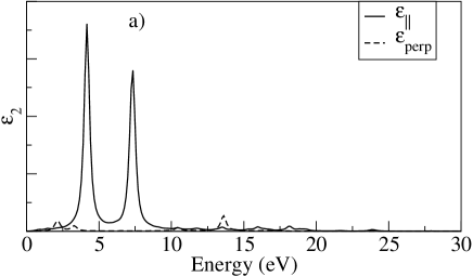
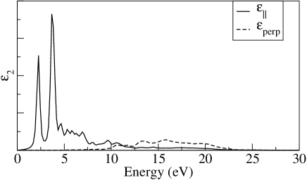
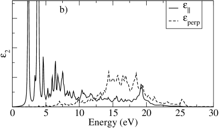
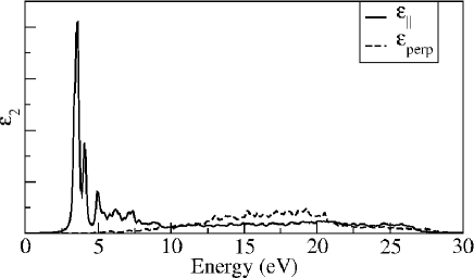
In anisotropic materials, dielectric properties must be described by the dielectric tensor. In Fig. 3 we show the average of the parallel and perpendicular directions of light polarization for using GW. Besides the results for bare bismuthene we show three showcases, two for a small ligands -C2H and CH3 for a larger ligand .
We identify a large anisotropy for bare and functionalized bismuth monolayers. This indicates a strong bismuth-bismuth hybridization within the basal plane, but smaller overlap perperdicular to the plane. Fig. 3(a) shows the results for bare bismuthene. The spectrum can be roughly divided into two main regions, around 4.2 and 7.3 eV. The is basically supressed. Upon adsorption of -H shifts of 2.3 and 3.7 eV as seen in Fig. 3(d) . Upon adsorption of groups, as shown in Fig. 3(c), peaks around 2.4 and 3.8 eV are seen. Another broad region between 6.0 and 8.0 eV is also presnet. There is a red shift implying that the system forms bonds. The shown in Fig. 3(d) has defined peaks centered around 2.1 and 3.2 eV. The general trend is the appearence of two distinct peaks. In functionalized bismuthene these two peaks appear are red-shift with respect to bare buckled bismuthene. The As the lattice constant increases, the spectrum is shifted to left, meaning that there is an interplay between size and reacitivity, as suggested for small ligands in germanene Jiang et al. (2013). Similarly, anisotropic and thickness-dependent optical properties of a two-dimenasiona layered monochalcogenide of germanium sulfide Research (2017) and black phosphorous Rudenko et al. (2015) has also been reported.
 |
 |
 |
 |
IV Conclusions
All the functional groups interact weakly with the bismuth surface. The transition from buckled to planar structure upon ligand adsorption is mainly due to the molecule-molecule interaction rather than the molecule substrate. This leads to a change in the electronic structure, yielding all the investigated groups as topological insulators. It is worth noting that lower coverages, where the ligand-ligand intercation is weaker, do not lead to buckled structures. The stability of these planar structures is mainly due by strain due to the ligand-ligand interaction rather than ligand-substrate interaction, meaning that the band gap of such systems can be tuned by chosing the appropriate ligand or molecule.
V Acknowledgements
We acknowledge the financial support from the Brazilian Agency CNPq and German Science Foundation (DFG) under the program FOR1616. The calculations have been performed using the computational facilities of Supercomputer Santos Dumont and at QM3 cluster at the Bremen Center for Computational Materials Science and CENAPAD.
References
- Geim and Novoselov (2007) A. K. Geim and K. S. Novoselov, Nature Materials 6, 183 (2007).
- Novoselov et al. (2004) K. Novoselov, A. Geim, S. Morozov, D. Jiang, Y. Zhang, S. Dubonos, I. Grigorieva, and A. Firsov, Science 306, 666 (2004).
- Caldwell et al. (2019) J. D. Caldwell, I. Aharonovich, G. Cassabois, J. H. Edgar, B. Gil, and D. N. Baso, Nat. Rev. Mat. p. 552–567 (2019).
- Schneider et al. (2018) C. Schneider, M. M. Glazov, T. Korn, S. Höfling, and B. Urbaszek, Nature Communication 9, 2695 (2018).
- Yang et al. (2020) F. Yang, A. O. Elnabawy, R. Schimmenti, P. Song, J. Wang, Z. Peng, S. Yao, R. Deng, S. Song, Y. Lin, et al., Nat. Comm. 11, 1088 (2020).
- Reis et al. (2017) F. Reis, G. Li, L. Dudy, M. Bauernfeind, Glass, W. Hanke, R. Thomale, J. Schäfer, and R. Claessen, Science p. 10.1126/science.aai8142 (2017).
- Ma et al. (2016) Y. Ma, Y. Dai, L. Kou, T. Heine, T. Frauenheim, and xx, Nano Letters p. 1083 (2016).
- Freitas et al. (2015) R. R. Q. Freitas, R. Rivelino, F. de Brito Mota, C. M. C. de Castilho, A. Kakanakova-Georgieva, and G. K. Gueorguiev, JPCC 119, 23599 (2015).
- Song et al. (2014) Z. Song, C.-C. Liu, J. Yang, J. Han, M. Ye, B. Fu, Y. Yang, Q. Niu, J. Lu, and Y. Yao, NPG Asia Materials 6, e147 (2014).
- Liu et al. (2017) M.-Y. Liu, Y. Huang, Q.-Y. Chen, Z.-Y. Li, C. Cao, and Y. He, RSC Advances 7, 39546–39555 (2017).
- Niu et al. (2015) C. Niu, G. Bihlmayer, H. Zhang, D. Wortmann, S. Blügel, and Y. Mokrousov, Phys. Rev. B 91, 041303(R) (2015).
- Jiang et al. (2013) S. Jiang, S. Butler, E. Bianco, O. D. Restrepo, W. Windl, and J. E. Goldberger, Nature Communications 5, 3389 (2013).
- Ren and andQian Niu (2016) Y. Ren and Z. Q. andQian Niu, Reports on Progress in Physic 79, 066501 (2016).
- Kowalczys et al. (2020) P. J. Kowalczys, S. A. Brown, T. Maerkl, Q. Lu, C.-K. Chiu, Y. Liu, S. A. Yang, X. W. nd Ilona Zasada, F. Genuzio, T. O. Mentes, et al., ACS Nano 14, 1888 (2020).
- Shiraz and Goh (2020) K. Shiraz and A. Y. Goh, phys. stat. sol. (b) 257, 190040 (2020).
- Hohenberg and Kohn (1964) P. Hohenberg and W. Kohn, Phys. Rev. 136, B864 (1964), URL http://link.aps.org/doi/10.1103/PhysRev.136.B864.
- Kohn and Sham (1965) W. Kohn and L. J. Sham, Phys. Rev. 140, A1133 (1965), URL http://link.aps.org/doi/10.1103/PhysRev.140.A1133.
- Perdew et al. (1996) J. P. Perdew, K. Burke, and M. Ernzerhof, Phys. Rev. Lett. 77, 3865 (1996), URL http://link.aps.org/doi/10.1103/PhysRevLett.77.3865.
- Kresse and Joubert (1999) G. Kresse and D. Joubert, Phys. Rev. B 59, 1758 (1999), URL http://link.aps.org/doi/10.1103/PhysRevB.59.1758.
- Shishkin et al. (2007) M. Shishkin, M. Marsman, and G. Kresse, Phys. Rev. Lett. 99, 246403 (2007), URL http://link.aps.org/doi/10.1103/PhysRevLett.99.246403.
- Blöchl (1994) P. E. Blöchl, Phys. Rev. B 50, 17953 (1994), URL http://link.aps.org/doi/10.1103/PhysRevB.50.17953.
- Hedin (1965) L. Hedin, Phys. Rev. 139, A796 (1965).
- Soluyanov and Vanderbilt (2011) A. A. Soluyanov and D. Vanderbilt, Phys. Rev. B 83 83, 235401 (2011).
- Gresch et al. (2017) D. Gresch, G. Autès, O. V. Yazyev, M. Troyer, D. Vanderbilt, B. A. Bernevig, and A. A. Soluyanov, Phys. Rev. B 95, 075146 (2017).
- Rosa et al. (2020) A. L. Rosa, E. N. Lima, M. C. da Silva, R. B. Pontes, T. M. Schmidt, and T. Frauenheim, J. Phys. Chem. C (2020).
- Ivanistsev et al. (2010) Ivanistsev, R. R. Nazmutdinov, and E. Lust, Surf. Sci. p. 1919 (2010).
- Kane (2013) C. L. Kane, Contemporary Concepts of Condensed Matter Science 6, 3 (2013), URL https://doi.org/10.1016/B978-0-444-63314-9.00001-9.
- Research (2017) N. Research, Nano Research pp. 546–555 (2017).
- Rudenko et al. (2015) A. Rudenko, S. Yuan, and M. Katsnelson, Phys. Rev. B 92, 085419 (2015).