Channeling experiments at planar diamond and silicon single crystals with electrons from the Mainz Microtron MAMI
Abstract
Line structures were observed for (110) planar channeling of electrons in a diamond single crystal even at a beam energy of 180 MeV. This observation motivated us to initiate dechanneling length measurements as function of the beam energy since the occupation of quantum states in the channeling potential is expected to enhance the dechanneling length. High energy loss signals, generated as a result of emission of a bremsstrahlung photon with about half the beam energy at channeling of 450 and 855 MeV electrons, were measured as function of the crystal thickness. The analysis required additional assumptions which were extracted from the numerical solution of the Fokker-Planck equation. Preliminary results for diamond are presented. In addition, we reanalyzed dechanneling length measurements at silicon single crystals performed previously at the Mainz Microtron MAMI at beam energies between 195 and 855 MeV from which we conclude that the quality of our experimental data set is not sufficient to derive definite conclusions on the dechanneling length. Our experimental results are below the predictions of the Fokker-Planck equation and somewhat above the results of simulation calculations of A. V. Korol and A. V. Solov’yov et al. on the basis of the MBN Explorer simulation package. We somehow conservatively conclude that the prediction of the asymptotic dechanneling length on the basis of the Fokker-Planck equation represents an upper limit.
1 Introduction
An intriguing field of research is intense radiation production with photon energies of 100 keV or more employing channeling of relativistic positrons or electrons with energies in the order of a few hundred MeV or higher. A very important prerequisite is the knowledge of the dechanneling length, i.e., the length before a charged particle is kicked out by a collision with an atom from the channel. Of particular interest are electrons since high quality electron beams can, in comparison with positron beams, much easier be supplied.
Currently simulation calculations are widely used to get information on dechanneling lengths also for bent crystals, see, e.g., the recent articles of A. V. Korol, A. V. Solov’yov et al. [1, 2]. Experimentally there are two possibilities to measure a dechanneling length. The first one is based on a variation of the thickness of straight crystals, the second one on the observation of dechanneled electrons in a bent crystal [3, 4]. This paper deals with the former possibility which we employed in previous experiments at MAMI to determine the dechanneling length for electrons in (110) silicon single crystals [5, 6]. Such kind of measurements were analyzed under various assumptions [7, 8, 9] which resulted in different dechanneling lengths.
In this paper we describe the continuation of such measurements on diamond single crystals at (110) planar channeling. Our main interest was whether quantum effects could enhance the dechanneling length at electron beam energies below about 200 MeV. In the first part of this paper we describe a measurement of the photon spectrum taken at (110) channeling at 180 MeV. This section is followed by a measurement of the dechanneling length at 450 and 855 MeV. The novel analysis method developed for this experiment has been employed also for a reanalysis of our previous measurements for (110) channeling at silicon single crystals.
2 Measurement of the photon spectrum for (110) planar channeling of 180 MeV electrons at diamond
The results of previous dechanneling length measurements for (110) silicon single crystals suggested that the dechanneling length enhances at beam energies below 200 MeV when compared with various theoretical predictions [9]. These findings were interpreted to originate from the occupation of deeply bound quantum states which require a rather large scattering angle in a single scattering event to achieve the energy transfer for dechanneling. Such processes may happen only in the tails of the scattering distribution function, and are, therefore, expected to be suppressed.
The existence of quantum states is well known from the observation of line structures at (110) channeling of electrons in diamond single crystals at beam energies between 53.2 to 110.2 MeV [10]. We supplemented the investigation with a measurement at a beam energy of 180 MeV. The deconvoluted spectrum is depicted in figure 1 (d).
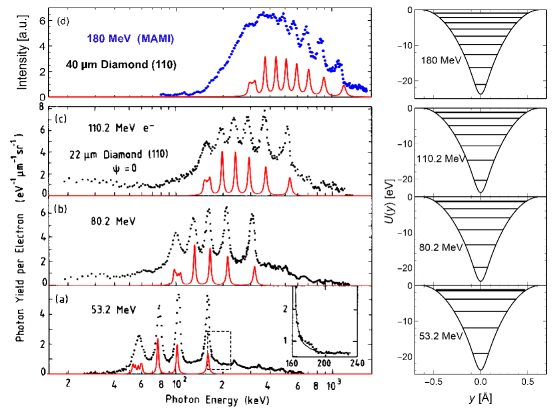
It shows that even at such a high beam energy line structures are present. This observation motivated us to initiate dechanneling length measurements as function of the beam energy also for diamond.
3 Dechanneling length measurements for diamond single crystals
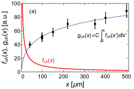
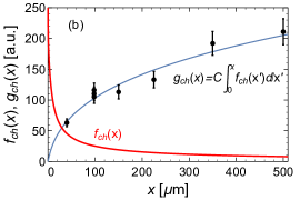
In order to investigate further whether the observation of line structures even at 180 MeV supports the picture of an enhanced dechanneling length, or not, we performed measurements for (110) planar channeling at diamond with the method described in [15]. The high energy loss signals generated at emission of a bremsstrahlung photon at channeling with an energy , is the beam energy, are depicted for various crystal thicknesses between 40 and 500 m by the error bars in figure 2. The signal is assumed to be proportional to the integral with the channel occupation probability. The question is now how to extract from the channel occupation probability as function of the crystal thickness a dechanneling length. Taking into account also rechanneling, one might try an ansatz with the aid of the ordinary differential equation
| (3.1) |
The problem with this ansatz is that the occupation probability depends, beside the dechanneling rate which is the quantity of interest, on equal footing also on the rechanneling rate . Obviously, the dechanneling rate cannot be extracted without additional assumptions. Because of lack of better theoretical data we utilized the solutions of the Fokker-Planck equation. How this has been performed will be described in the next section.
4 Fokker-Planck equation for a plane crystal
In the analysis of our experiments we take advantage of numerical solutions of the Fokker-Planck equation, see e.g. [16, 17, 18]. Well adapted for our purpose are descriptions in [7, 8, 9]. A coordinate system has been chosen with the axis pointing into the initial beam direction, and the axis perpendicular to the channeling planes. The Fokker-Planck equation with the probability density and the probability current written with the normalized variables and reads with the diffusion coefficient and the time period
| (4.1) |
| (4.2) |
| (4.3) |
The integration limits and are the roots of the equation . The two normalizing variables are the depth of the potential , and the scaling length
| (4.4) |
The quantity = 0.1213 m is the radiation length [19], the momentum of the electron, its total energy, c the speed of light, , the velocity of the electron, and = 0.0423 Å the standard deviation of the one dimensional thermal vibration amplitude at 293 K with Å2 according to [20, equation (15)]. The quantity = 1.261 Å in the nominator of the integral in equation (4.2) is the (110) interplanar distance, with = 3.567 Å the lattice constant at 300 K, taken from [21, 22]. All numbers are given for diamond.
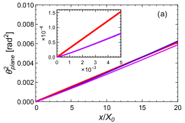
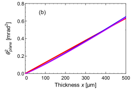
Equation (4.4) is exactly the expression which Baier et al. quote for the dechanneling length [16, eqn. (10.1)], however, here with a modified = 10.6 MeV valid for small thicknesses . For the reasoning see figure 3.
From a solution of the Fokker-Planck equation the channel occupation probability can be calculated with the integral
| (4.5) |
It depends on the dechanneling and rechanneling currents and across the continuum border from which transition rates for de- and rechanneling rates can be calculated as
| (4.6) |
| (4.7) |
By means of the relation , which also defines the drift coefficient , the current in equation (4.1) has been subdivided into a diffusion and a drift current :
| (4.8) |
The Heaviside function takes into account that for the diffusion current is outward directed, i.e., it contributes to the dechanneling rate with vanishing rechanneling, see figure 4.
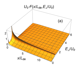

It appears that for small thicknesses an equilibration phase exists which depends on the angular spread of the incoming electron beam and lasts for the example of rad about one dechanneling length, . From this discussion we may conclude that the solution for small penetration depths is probably rather inaccurate.
Several other interesting features can be recognized from figure 4 (b). Most important is that the dechanneling rate scales in both coordinates with the scaling length . Asymptotically the normalized de- and rechanneling rates approach numbers which are close to, but not exactly, unity, for numerical values see caption of figure 4. We further mention that for large the absolute values of the transition rates approach each other with the diffusion rate always somewhat smaller. Qualitatively it can be concluded from equation (4.4) that for a large dechanneling length the beam energy , potential depth , and the radiation length all should be large.
5 Analysis procedure and results
In the analysis we assumed that the difference can be taken from the Fokker-Planck equation. This assumption may well be allowed for the beam eneries of 450 and 855 MeV for which quantum state effects most likely are not of importance. The factor in equation (3.1) has been treated as a fit parameter. The experimental dechanneling length is with . In figure 2 (a) and (b) the results of the best fits procedures are shown. Figure 5 (a) depicts the dechanneling lengths for the two beam energies of 450 and 855 MeV. Because of technical reason during the course of the experiment we could not take data for the most interesting beam energy of 180 MeV. Therefore, we also reanalyzed with the same method older measurements for (110) channeling at silicon single crystals. The results are shown in figure 5 (b). The conjectured effect was not found.
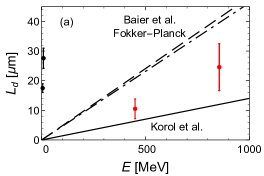
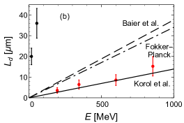
It can be seen from figure 5 (a) and (b) that large deviations of the theoretical predictions for the dechanneling lengths exist which, consequently, are also expected for the difference in the transition rates . However, such a possibility is partly taken into account in the best fit procedure by the parameter in equation (3.1). As mentioned, for thicknesses the accuracy of obtained from the Fokker-Planck equation might be questionable. To estimate the sensitivity, the rechanneling curve has been shifted by which resulted in a change of the asymptotic dechanneling length in the order of 30 % which has been taken into account in the error bars of figure 5.
6 Discussion and conclusion
Some remarks of caution on our previous measurements for (110) channeling at silicon for beam energies between 195 and 855 MeV and the analysis of these data may be appropriate. We would like to stress that the signals observed for diamond shown in figure 2 do not saturate as function of the crystal thickness what was not observed for silicon [5, 6]. Since we concluded from such a saturation evidence for quantum states effects, the experiment on diamond casts serious doubts on the assumptions made in our previous analysis [9]. Assuming that the classical picture must be favored, our current model assumptions seem to be more realistic. However, we must concede that much more accurate experimental data are required to validate on the basis of a analysis certain model assumptions, or exclude others. Also the experiment on diamond, see figure 2, must be improved. In this context we mention that the various crystals used for the measurement may scatter in quality, meaning that, e.g., the dislocation density may vary from crystal to crystal, and in turn also the signals obtained for a dechanneling length measurement. Such a possibility has been partly included into the error bars in figure 2.
The most striking feature of the theoretical curves in figure 5, black lines, is the fact that the dechanneling lengths on the basis of the Fokker-Planck equations (4.1) and the simulation calculations of Korol et al. [1, 2] disagree by a large factor. We can discuss this deviation on a safe ground only for the solution of the Fokker-Planck equation.
First of all one might question the prerequisite of the Fokker-Planck equation for which statistical equilibrium has been assumed meaning that the probability distribution in a channel is represented by
| (6.1) |
For this function has singularities which turn out to be harmless for the calculation of the diffusion coefficients or for the solution of the Fokker-Planck equation. In particular, the probability currents which enter the transition rates are smooth as function of . However, the singularities push the probability density towards the potential walls resulting in particular for deeply bound electrons in a reduction at the center where the scattering centers are located. The effect is rather large, e.g., for the total probability reduces from 1 to 0.67 at integration between 90 % of and . As a consequence, the calculated diffusion coefficients which enter into the Fokker-Planck equation may be too small, and in turn also the transition rates.
Further effects will be discussed by means of the scaling length , equation (4.4). We recognize that the most sensitive parameter is since it enters quadratically. To explain a factor of even 2.5 we would have to assume an MeV which can be ruled out by the same argumentation carried out above in figure 3 (inset). There remains the potential depth to be discussed. The potential has been calculated in the Doyle-Turner [12] and in the Molière approximation, the latter with the parameter set of [16, p.199 and 235]. We calculated for values of 22.41 eV (Molière) and 23.42 eV (Doyle-Turner) for (110) diamond, and 22.61 eV (Molière) and 21.09 eV (Doyle-Turner) for (110) silicon, i.e., the agreement is better than 7.2%. Therefore, it is hard to conceive that the potentials are wrong by about a factor of two.
From figure 4 we see already qualitatively that a large fraction of electrons are weakly bound. Indeed 24 % of all electrons have a binding energy of less than 10 % of . Those electrons may be excited into the continuum by electron-electron interactions. The latter is not included into , but it has been mentioned in [9] that the effect on the dechanneling length would be in the 10 % range. However, the electron density between the planes may well be different as it was calculated from the Molière potential. We also mention an additional idealization namely that in the Molière potential the microscopic atomic structure of a plane is averaged out. Any wavy structure may cause an additional dechanneling contribution by the accompanied Fourier frequency spectrum the channeled electron experiences.
Whether the discussed effects may decrease the dechanneling length by a factor in the order of two or three, or not, remains an open question. At the time being we somehow conservatively conclude that the prediction of the asymptotic dechanneling length on the basis of the Fokker-Planck equation represents an upper limit.
Acknowledgments
One of us (H.B.) acknowledges the hospitality of Professor Dr. Vadim Ivanov and Dr. Andrei Korol during his one month stay at the Peter The Great St. Petersburg Polytechnic University in April and June 2017. Many fruitful discussions, in particular with Andrei Korol, were of crucial importance for this work and are gratefully acknowledged.
This work has been supported by the European Commission (the PEARL Project within the H2020-MSCA-RISE-2015 call, GA 690991).
References
- [1] A. V. Korol, V. G. Bezchastnov, G. B. Sushko and A. V. Solov’yov, Simulation of channeling and radiation of 855 MeV electrons and positrons in a small-amplitude short-period bent crystal, Nuclear Instruments and Methods in Physics Research B 387 (2016) 41.
- [2] A. V. Korol, V. G. Bezchastnov and A. V. Solov’yov, Channeling and radiation of the 855 MeV electrons enhanced by the re-channeling in a periodically bent diamond crystal, THE EUROPEAN PHYSICAL JOURNAL D 71 (2017) 174.
- [3] A. Mazzolari, E. Bagli, L. Bandiera, V. Guidi, H. Backe, W. Lauth et al., Steering of a Sub-GeV Electron Beam through Planar Channeling Enhanced by Rechanneling, Physical Review Letters 112 (2014) 135503.
- [4] T. N. Wistisen, U. I. Uggerhøj, U. Wienands, T. W. Markiewicz, R. J. Noble, B. C. Benson et al., Channeling, volume reflection, and volume capture study of electrons in a bent silicon crystal, Physical Review Accelerators and Beams 19 (2016) 071001 11 pages.
- [5] W. Lauth, H. Backe, P. Kunz and A. Rueda, Channeling Experiments with Electrons at the Mainz Microtron MAMI, in Charged and Neutral Particles Channeling Phenomena, Channeling 2008, Proceedings of the 51st Workshop of the INFN ELOISATRON Project, Erice, Italy 15 October - 1 November 2008, S. B. Dabagov, L. Palumbo and A. Zichichi, eds., The Science and Culture Series - Physics, (World Scientific Publishing Co. Pte. Ltd., 5 Toh Tuck Link, Singapore 596224), pp. 335–342, World Scientific: New Jersey, London, Singapore, Beijing, Shanghai, Hong Kong, Taipei, Chennai, 2008.
- [6] W. Lauth, H. Backe, P. Kunz and A. Rueda, Channeling Experiments with Electrons at the Mainz Microtron MAMI, International Journal of Modern Physics A 25, Supplement 1 (2010) 136.
- [7] H. Backe, P. Kunz, W. Lauth and A. Rueda, Planar channeling experiments with electrons at the 855 MeV Mainz Microtron MAMI, Nuclear Instruments and Methods in Physics Research B 266 (2008) 3835 .
- [8] H. Backe, D. Krambrich, W. Lauth, K. Andersen, J. L. Hansen and U. I. Uggerhøj, Radiation emission at channeling of electrons in a strained layer Si1-xGex undulator crystal, Nuclear Instruments and Methods in Physics Research B 309 (2013) 37 .
- [9] H. Backe and W. Lauth, Channeling experiments with sub-GeV electrons in flat silicon single crystals, Nuclear Instruments and Methods in Physics Research B 355 (2015) 24.
- [10] M. Gouanere, D. Sillou, M. Spighel, N. Cue, M. J. Gaillard, R. G. Kirsch et al., Planar channeling radiation from 54-110-MeV electrons in diamond and silicon, Physical Review B 37 (1988) 4352 .
- [11] B. Azadegan, A Mathematica package for calculation of planar channeling radiation spectra of relativistic electrons channeled in a diamond-structure single crystal (quantum approach)), Computer Physics Communications 184 (2013) 1064.
- [12] P. A. Doyle and P. S. Turner, Relativistic Hartree-Foek X-ray and Electron Scattering Factors, Acta Crystallographica A 24 (1968) 390.
- [13] R. Pantell, J. Kephard, R. Klein, H. Park, B. Berman and S. Datz, The Study of Material Properties Using Channeling Radiation, in Relativistic Channeling, Proceedings of a NATO Advanced Research Workshop on Relativistic Channeling, March 31 - April 4, 1986 at Villa Del Mare, Acquafredda di Maratea, Italy, J. R.A. Carrigan and J. Ellison, eds., NATO Advanced Science Institutes Series (ASI), (A Division of Plenum Publishing Corporation, 233 Spring Street, New York, N.Y. 10013), pp. 435–453, Plenum Press, New York and London, 1987.
- [14] A. Pathak and S. Satpathy, Crystal Potentials from Channeling, in Relativistic Channeling, Proceedings of a NATO Advanced Research Workshop on Relativistic Channeling, March 31 - April 4, 1986 at Villa Del Mare, Acquafredda di Maratea, Italy, J. R.A. Carrigan and J. Ellison, eds., NATO Advanced Science Institutes Series (ASI), (A Division of Plenum Publishing Corporation, 233 Spring Street, New York, N.Y. 10013), pp. 455 – 458, Plenum Press, New York and London, 1987.
- [15] H. Backe, D. Krambrich, W. Lauth, K. K. Andersen, J. L. Hansen and U. I. Uggerhøj, Channeling and Radiation of Electrons in Silicon Single Crystals and Si1-xGex Crystalline Undulators, Journal of Physics: Conference Series 438 (2013) 012017.
- [16] V. N. Baier, V. M. Katkov and V. M. Strakhovenko, Electromagnetic Processes at High Energies in Oriented Single Crystals. World Scientific, Singapore, New Jersey, London, HongKong, World Scientific Publishing Co. Pte. Ltd, P O Box 128, Farrer Road, Singapore 912805, 1998.
- [17] V. V. Beloshitsky and C. G. Trikalinos, Passage and radiation of relativistic channeled particles, Radiation Effects 56 (1981) 71.
- [18] M. A. Kumakhov and F. F. Komarov, Radiation from charged particles in solids. American Institute of Physics New York, , 1989.
- [19] C. Patrignani and et al. (Particle Data Group), Table 6. Atomic and Nuclear Properties of Materials, Chin. Phys. C 40 (2016 and 2017 update) 100001.
- [20] V. F. Sears and S. A. Shelley, Debye-Waller Factor for Elemental Crystals, Acta Crystallographica A 47 (1991) 441.
- [21] Vadim Siklitsky and Alexei Tolmatchev (Ioffe Physico-Technical Institute), “Electronic archive: New Semiconductor Materials. Characteristics and Properties.” http://www.ioffe.ru/SVA/NSM/Semicond/Diamond/basic.html, 1998-2001.
- [22] “New Semiconductor Materials. Biology systems. Characteristics and Properties.” http://www.matprop.ru/Diamond_basic.
- [23] B. Rossi and K. Greisen, Cosmic-Ray Theory, Review of Modern Physics 13 (1941) 240.
- [24] G. Lynch and O. Dahl, Approximations to multiple Coulomb scattering, Nuclear Instruments and Methods in Physics Research B 58 (1991) 6.
- [25] U. Nething, M. Galemann, H. Genz, M. Hofer, P. Holfmann-Stascheck, J. Hormes et al., Intensity of Electron Channeling Radiation and Occupation Lengths in Diamond Crystals, Physical Review Letters 72 (1994) 2411.
- [26] J. O. Kephart, R. H. Pantell, B. L. Berman, S. Datz, H. Park and R. K. Klein, Measurement of the occupation lengths of channeled 17-MeV electrons and 54-MeV electrons and positrons in silicon by means of channeling radiation, Physical Review B 40 (1989) 4249 .