Nematicity and Competing Orders in Superconducting Magic-Angle Graphene
Abstract
Strongly interacting electrons in solid-state systems often display tendency towards multiple broken symmetries in the ground state. The complex interplay between different order parameters can give rise to a rich phase diagram. Here, we report on the identification of intertwined phases with broken rotational symmetry in magic-angle twisted bilayer graphene (TBG). Using transverse resistance measurements, we find a strongly anisotropic phase located in a ‘wedge’ above the underdoped region of the superconducting dome. Upon crossing the superconducting dome, a reduction of the critical temperature is observed, similar to the behavior of certain cuprate superconductors. Furthermore, the superconducting state exhibits a anisotropic response to an directional-dependent in-plane magnetic field, revealing a nematic pairing state across the entire superconducting dome. These results indicate that nematic fluctuations might play an important role in the low-temperature phases of magic-angle TBG, and pave the way for using highly-tunable moiré superlattices to investigate intertwined phases in quantum materials.
I Introduction
Spontaneous symmetry breaking is a ubiquitous process that occurs at all length scales in nature1, from the endowment of mass to elementary particles through the Higgs mechanism, the emergence of ferromagnetism and superconductivity in mesoscopic and macroscopic systems, all the way to the creation of stars and galaxies in the early universe. In a solid-state system, besides time-reversal and gauge symmetries, there are certain discrete symmetries imposed by the underlying crystal lattice. However, these symmetries can be spontaneously broken when many-body electron-electron interactions in the system are significant. Studying these broken-symmetry states is fundamental to elucidate the various phases in these many-body systems 3; 2. One example is an electronic nematic phase, where the discrete rotational symmetry of the lattice is spontaneously broken due to electron correlations, while lattice translational and time-reversal symmetries are preserved 4; 5. The resulting anisotropy of the system is in turn manifested in the spin, charge, and lattice degrees of freedom, and can be measured via scattering, transport and scanning probe experiments. 8; 9; 10; 6; 7; 11
When a correlated system has multiple broken-symmetry phases, their relationship often goes beyond mere competition, giving rise to a complex phase diagram of intertwined phases 12; 13; 14. For example, in the underdoped region of the phase diagram of certain cuprate superconductors, a depletion in the critical temperature is found near , where is the hole doping concentration 15. This observation is typically attributed to the competition between superconductivity and a stripe phase that has spin and/or charge ordering 15; 2; 16 Charge order and superconductivity may also intertwine to form a pair density-wave state 13; 17. Another example of intertwined order is a nematic superconducting state, which simultaneously breaks lattice rotational and gauge symmetries. Nematic pairing states have been reported in certain iron pnictides and in doped Bi2Se3, as revealed by thermal, magnetic, and transport measurements 18; 20; 21; 19; 22; 23; 24, although their microscopic origin is still unclear.
The recent discovery of correlated insulator and superconducting behaviors 25; 26 in two-dimensional (2D) graphene superlattices brings the possibility of studying correlated superconducting materials with unprecedented tunability and richness. Twisted 2D materials exhibit long-range moiré patterns in real space that can be tuned by the twist angle (Fig. 1a). In twisted bilayer graphene (TBG) near the first magic-angle , the interlayer hybridization results in nearly-flat bands at low energies, in which the electrons are localized in real space (Fig. 1a).27; 28; 29 Near half-filling of the nearly-flat bands, correlated insulator behavior and superconductivity have been demonstrated.25; 26; 30 These emergent states likely originate from strong electron-electron interactions in the nearly-flat bands. In this work we study the interplay between the superconducting phase and other many-body phases in magic-angle TBG. Compared to conventional materials, a major advantage of magic-angle TBG is that the band filling can be continuously tuned by electrostatic gating instead of chemical doping, so that different phases can be accessed in a single device.
II Results
In this article, we investigate the phase diagram of magic-angle TBG in detail, focusing particularly on anisotropic properties in the superconducting and normal phases. We uncover an anisotropic in-plane electrical transport in magic-angle TBG at low temperatures using longitudinal and transverse resistivity measurements. In addition, we reveal an anisotropic in-plane critical field and an anistropic response of the superconducting critical current to an in-plane magnetic field. Our results show that magic-angle TBG can spontaneously break lattice rotational symmetry in both the normal and superconducting phases, although the anisotropic properties of these two states are manifested in different observables, suggesting that the origins of these two anisotropic states might be different.
II.1 Characterization of Magic-angle Graphene
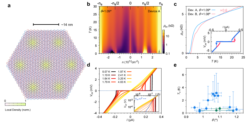
Using the previously developed ‘tear and stack’ dry-transfer technique 32; 31, we fabricate high quality encapsulated TBG devices with twist angles around the first magic angle . The main devices we report about are devices A and B, with twist angles of and , respectively. The low-energy bands in TBG are four-fold degenerate (due to spin and valley degrees of freedom) and can sustain an electron density of , where is the area of a moiré unit cell. This density corresponds to filling four electrons or holes per moiré unit cell. Near the first magic angle, correlated states can form at integer electron fillings of the moiré superlattice, i.e. when . This is believed to be a consequence of the fact that the electronic interactions become comparable to the bandwidth of the nearly-flat bands. In the resistivity measurements of device A shown in Fig. 1b, we indeed find an enhancement of the resistivity at all these integer fillings. A superconducting dome is recognizable upon hole-doping of the insulating state, at temperatures below . Fig. 1c shows the curves of device A and device B at their optimal doping levels (highest ). Both devices exhibit a relatively high in the range of (at normal resistance) 33. Figure 1d shows the evolution of the - curves with temperature. From the log-log plot shown in the inset, we can extract the Berezinskii-Kosterlitz-Thouless (BKT) transition temperature to be . Devices A and B have in fact some of the highest transition temperatures among all reported magic-angle TBG devices so far, as evident from the statistics shown in Fig. 1e, as well as devices reported in the literature 26; 30; 34.
II.2 Anisotropic Behavior in the Normal Phase
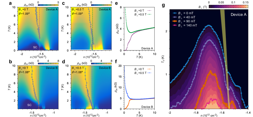
Figs. 2a-b show the resistivity versus gate-induced density, , and temperature, , maps of devices A and B, respectively, in the vicinity of . We find that in both devices the region of the phase diagram has a rather complicated structure. As can be seen in Figs. 2a-b, there are two resistive features in the normal state: one ‘wedge’-like feature above the superconducting dome (near for device A and for device B) that bends at elevated temperatures, and one resistive feature on the right hand side of the dome (near for both devices). While the latter feature corresponds to the state similar to the correlated states previously reported in magic-angle TBG 25; 26; 30; 34, the wedge-like feature creates a noticeable ‘kink’ (i.e. decrease in ) where it intersects with the superconducting dome. This suppression of resembles that observed in underdoped cuprates, where it is attributed to a spin/charge ordered phase that competes with superconductivity 15; 2; 16. To further probe the resistive wedge-like feature, we apply a small perpendicular magnetic field to fully suppress superconductivity, as shown in Figs. 2c-d. Line cuts of the resistivity versus temperature at the densities corresponding to the ‘kinks’ of are compared in Figs. 2e-f for the two devices. It can be clearly seen that when superconductivity is suppressed, the resistive wedge-like feature turns insulating upon approaching zero temperature. A small magnetic field thus results in a superconductor-to-insulator transition at this density. In Fig. 2g, we show the gradual suppression of by the perpendicular magnetic field from zero to in device A. We find that above about , the superconducting dome splits at into two domes. This density approximately coincides with the density where the wedge-like feature extrapolates to zero temperature. The separated domes are centered at around and respectively. The position of the splitting point corresponds to hole doping with respect to the correlated insulator state. These findings are reminiscent of the recently reported high-field experiments in underdoped cuprates, where the superconducting dome splits at hole-doping in a magnetic field 35, suggesting that a quantum critical point might also exist in the phase diagram of magic-angle TBG.
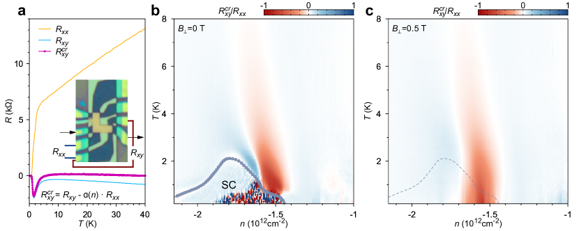
To gain more insight into the possible origin of the resistive wedge-like feature, we measure the transverse voltage across the sample at zero magnetic field, which gives us the transverse resistance 36; 37. In an anisotropic conductor in two dimensions, the 2-by-2 resistivity tensor has two diagonal components . If the major axis of the anisotropy (usually one of the crystal axis) is not aligned with the reference frame of the tensor, the off-diagonal terms of the resistivity tensor are proportional to , where is the angle between the anisotropy axis and the reference -axis (see Supplementary33 for derivation). As a result, when an electrical current flows in the direction, a transverse voltage appears across the edges perpendicular to the axis, giving a nonvanishing as long as and . The first condition is assumed to be true in our experiment, since the lattice orientation is random with respect to the sample edge. Consequently, a non-vanishing transverse resistance in our experiment implies anisotropic resistivity, , and therefore the breaking of the six-fold rotational symmetry of TBG. Note that this transverse voltage is fundamentally different from the Hall effect since time-reversal symmetry is not broken. In order to quantitatively analyze the transverse voltage, we need to remove any residual longitudinal component that might appear in the transverse voltage due to imperfect alignment of the four-probe voltage contacts and/or sample inhomogeneity.36; 33 Fig. 3a shows the raw and measured for device A near the wedge-like feature, as shown in Fig. 2a. At high temperatures (), where the anisotropies associated with electron correlation effects are presumably overwhelmed by thermal fluctuations, both and are linear in and proportional to each other: .36 To correct for this background signal that is likely a result of the imperfect voltage probe alignment, we subtract this component from so that at the highest temperature of the net signal is zero. This corrected transverse voltage , where is a density-dependent numerical factor typically within , constitutes a truthful measure of the resistivity anisotropy (purple curve in Fig. 3a). We note that, while no signal is present at higher temperatures, below there is a significant negative peak in , which indicates the onset of anisotropy at this temperature.
The gate and temperature dependence of the anisotropy, shown in Figs. 3b-c for zero magnetic field and (see Supplementary33), clearly reveals a prominent anisotropy ‘wedge’ as well. The transverse voltage measured at is symmetrized with data measured at to remove the contribution from the Hall voltage. Here we plot the normalized quantity , which is approximately proportional to the anisotropy ratio (see Supplementary 33). We also mark out the superconducting dome in Fig. 3b-c. Immediately above the superconducting dome on the ‘underdoped’ side (lower ), we find a strong transverse voltage signal with a sign change at around (see the supplementary for other ranges of density).33 The position of the anisotropy wedge matches well with the resistive wedge-like feature that we observed in Fig. 2a. The sign change indicates that the anisotropy changes from to (or vice versa). In (Fig. 3c), the anisotropy wedge with negative values of persists to zero temperature, consistent with the behavior of the resistive wedge-like feature in Fig. 2b as well. On the other hand, we notice that the anisotropy with positive near disappears as superconductivity is suppressed by the magnetic field, which might be explained by the vestigial order from the nematic superconductivity that will be discussed in the next section.
II.3 Nematic Superconducting State
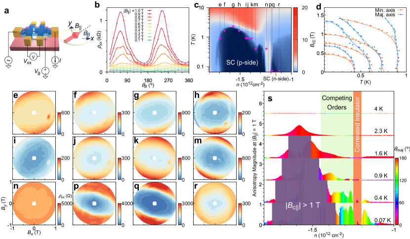
A natural question to ask is whether the superconducting phase exhibits any anisotropic properties as well. To investigate this, we measure the angle-dependent in-plane magnetic field response of the superconducting phase. In magic-angle TBG, the superconductivity is suppressed by an in-plane magnetic field of the same order of magnitude as the Pauli paramagnetic limit 26. Using a vector magnet in a dilution refrigerator, we apply a magnetic field up to in an arbitrary direction within the sample plane (see Fig. 4a for illustration). We compensate for possible sample tilt by applying a small out-of-plane magnetic field, so that the magnetic field is parallel to the sample to within at (see Supplementary33 for detailed calibration procedure). Figure 4b shows an example of the resistivity versus in-plane magnetic field magnitude and angle (with respect to the length of the Hall bar, see Fig. 4a). A two-fold anisotropic suppression of the superconductivity can be clearly seen. We have checked that the direction of the current flow is not correlated with the anisotropy direction, and therefore the anisotropic Lorentz force contribution can be excluded.33 The anisotropy is not aligned with the length or width of the Hall bar either.33
The two-fold anisotropy of the in-plane magnetotransport response points towards nematicity that is intrinsic to the superconducting phase, since it breaks the six-fold rotational symmetry of the moiré superlattice. We have systematically studied this nematic behavior across the entire superconducting dome of device B. In Figs. 4e-r we show polar maps of the magneto-resistivity at different carrier densities in the hole-doping and electron-doping superconducting domes as labeled in Fig. 4c. At all densities except those in Figs. 4n and r, we find elliptic contours that have major/minor axis ratio up to . Note that we chose to always measure near , since deep inside the superconducting dome the in-plane critical field is usually larger than and cannot be measured in our setup. However, we have confirmed the nematicity in the region by simultaneously applying a small perpendicular field to partially suppress the superconducting state.33 At the densities corresponding to Figs. 4n and r, which are outside the superconducting regions, the anisotropy is essentially nonexistent. In device A, we have also observed similar two-fold anisotropic in-plane critical field (Fig. 4d). The critical magnetic field along the major axis extrapolated to zero temperature exceeds that along the minor axis by in this device.
Fig. 4s shows the evolution of the magnitude and of the director of the nematic component of the superconducting state in device B as a function of carrier density and temperature. Our data shows that the nematic director, as measured by the angle of rotation of the ellipse’s major axis, does not appear to be exactly locked to any particular spatial axis, but instead evolves continuously with carrier density. In particular, in the superconducting dome on the hole-doping side of , the direction of the major axis varies slowly within in the density range of (corresponding to the ellipses from Fig. 4e to 4h), while in the range of (from Fig. 4i-m) the major axis rotates quickly with the carrier density. From Fig. 4i to Fig. 4m, the major axis rotates by . We note that the latter range of density again coincides with the resistive wedge-like feature for device B, as shown from Figs. 2b and d. The smaller superconducting dome on the electron-doping side near exhibits significant nematicity as well (Fig. 4p and q), with a director pointing from to . As we explain below, the fact that the nematic director changes direction as a function of doping makes it unlikely that the superconducting anisotropy is simply a response to strain present in the sample. On the contrary, this observation is consistent with spontaneous rotational symmetry-breaking characteristic of an intrinsic nematic superconductor.
II.4 Anisotropic Response of the Superconducting Gap
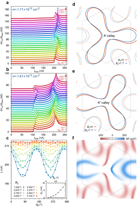
The observation of nematicity puts certain constraints on possible pairing symmetries of the superconducting order parameter.14; 39; 38 One can obtain information about the superconducting gap by measuring the critical current . Here, by measuring of device B in the presence of in-plane magnetic fields, we demonstrate that the nematicity is not only manifested in the resistivity measurements, but also creates an anisotropic modulation of the superconducting gap. Figs. 5a-b show the waterfall plots of differential resistance versus dc bias current at two carrier densities, in an in-plane magnetic field along different directions indicated by the colors. At the carrier density in Fig. 5b, the plot shows two critical currents at and respectively, which might be due to domains in the device with different twist angles or nematic directors. Interestingly, at both carrier densities the critical current shows significant two-fold modulation by the in-plane magnetic field direction . The dependence can be fit by a sinusoidal function (Fig. 5c), where is the direction of the major axis. The modulation amplitude as a function of the in-plane field magnitude is shown in the inset of Fig. 5c, and follows an approximately quadratic power law dependence.
An anisotropic response in the critical current may originate from (i) the superconducting gap and/or (ii) anisotropic properties of the underlying normal state (). Although we have shown that the normal state exhibits considerable resistance anisotropy at densities near the wedge-like feature in Fig. 3, we argue here that the anisotropic response of the critical current is not a result of the anisotropy of . First, Fig. 5a is measured at a density for which there is essentially no resistivity anisotropy in the normal state ( at the lowest in Fig. 3c), while Fig. 5b is measured at one with significant anisotropy in the normal state ( at the lowest in Fig. 3c). However, the modulation of the critical current at these two densities shows similar magnitudes. Second, an anisotropy in the resistivity tensor may not necessarily imply a large anisotropic response of the resistivity versus in-plane magnetic field. In fact, as we show in the Supplementary, inside the wedge-like feature in the normal state in device A, we could not measure significant anisotropic response to the in-plane field. Thus, these results suggest that the anisotropic response of the critical current might not be directly related to the resistivity anisotropy of the normal state and hence may originate from an anisotropic superconducting gap.
To discuss the mechanism by which the in-plane field couples to the superconducting gap, we note that if the former couples solely to the spin degree of freedom (and thus the gap is only suppressed by the Zeeman coupling), spin-orbit interaction must be introduced to explain the dependence of on the direction of . However, the intrinsic spin-orbit coupling in graphene-based systems is known to be very weak. We might consider the following mechanism to reconcile these facts. As illustrated in Fig. 1a, the unit cell of magic-angle TBG has a length scale of . Despite the separation between the graphene sheets in TBG being merely , an in-plane magnetic field penetrating them induces a small but non-negligible magnetic flux in the cross-section of the unit cell with an area , which modifies the Fermi contours. To demonstrate this effect, we numerically calculated the Fermi contours at for and along the direction using the Bistritzer-MacDonald continuum model 28. Figs. 5d and 5e show the original and modified Fermi contours for the and valleys respectively. As can be seen from the contours, a noticeable shift is induced by the in-plane magnetic field. The / valley degeneracy is lifted by the momentum shift between the two layers introduced by the in-plane field, which is proportional to , a substantial shift given the small size of the Brillouin zone. If one assumes that only electrons with opposite momentum and valley are allowed to form Cooper pairs in the superconducting phase, the two states from opposite valleys would be at slightly different energies when an in-plane field is applied, which serves to suppress the superconductivity in a similar fashion as the paramagnetic (Zeeman) effect in the case of spins. To more intuitively demonstrate this, Fig. 5f shows the de-pairing energy along the Fermi contour . It is strongly directional dependent and has a similar order of magnitude as the Zeeman energy at ( where , is the Bohr magneton). The de-pairing energy exhibits a six-fold variation with respect to the direction of the in-plane magnetic field, while the nematic component of the superconducting order can further spontanously break this symmetry down to the observed two-fold symmetry 42; 39; 41. A small strain can further assists to pin down the nematic domain along a given direction.
III Discussion
Our measurements reveal two distinct anisotropic states in the phase diagram of magic-angle TBG: a normal-state wedge-like feature above the superconducting dome and a nematic pairing state. As shown by the longitudinal resistivity and transverse voltage measurements presented in Fig. 2 and Fig. 3, the wedge-like feature is associated with a zero-temperature insulating phase that shows significant resistivity anisotropy, indicative of broken six-fold lattice rotational symmetry. Thus, this normal state phase might be either an electronic nematic state or an electronic smectic state – i.e. a charge or spin density-wave that, in addition to rotational symmetry, also breaks translational lattice symmetry. In either case, the rotational symmetry-breaking can be described by a two-component 3-state Potts nematic order parameter , with restricted to three possible values 43; 41. Electronic correlations might be important for the formation of such a state. Twisted bilayer graphene is well-known to exhibit van Hove singularities (vHs), which in general do not occur exactly at half-filling 44; 45. Near the vHs, it has been theoretically shown that the significant nesting between the - and -valley Fermi contours might induce density wave ordering 38. Remarkably, recent scanning tunneling experiments have identified prominent rotational-symmetry-broken features in the normal state local density of states,46; 47; 48. Alternatively, strong-coupling models can also yield nematic and density-wave states 49; 50. Importantly, the fact that only one dominant nematic domain is observed implies the existence of some small residual strain in the device, which selects that particular domain. One can rule out the scenario in which the anisotropic state itself is a trivial consequence of such a strain, because the wedge-like feature is restricted to narrow temperature and doping ranges. In contrast, strain-induced anisotropy should persist at all temperatures and over a much wider doping range.
For the superconducting phase, its remains to be seen whether its nematic character, as revealed by the measured in-plane anisotropy of the critical field, can be reconciled with -wave pairing. On the other hand, it may be more naturally explained in terms of a two-component -wave/-wave gap of the form , indicative of an unconventional pairing mechanism 51. Here, the parameter , responsible for the breaking of the six-fold rotational symmetry, is associated with the orientation of the ellipses in Fig. 4 (Ref.42). The fact that only one orientation is observed for a given doping suggests that strain is pinning it. However, because the ellipse orientation rotates continuously over the doping range , we can conclude that the anisotropy of the superconducting state is intrinsic, i.e. it would be present even for zero strain. To see this, we follow Ref. 41 and note that, to lowest order in a free-energy expansion, uniaxial strain couples to the superconducting order parameter as , where is the direction strain is applied. This term alone only allows two possible relative orientations between and , namely, and , depending on the sign of (i.e. compressive or tensile strain). Thus, because for a given device is presumably fixed, we would expect the same ellipse orientation for all doping levels. However, if breaks the rotational symmetry on its own (i.e without strain), the free energy has another relevant term . In the absence of strain, this term fixes to three values (modulo ). When combined with the strain-coupling term of the free energy, it allows to continuously rotate within a range of values, which depend on phenomenological parameters. While a more detailed analysis is presented in the supplementary material, the simple fact that the ellipses orientations are not the same for all doping levels provides strong evidence that the nematic superconductivity is an intrinsic property of magic-angle TBG. Indeed, nematicity is observed essentially across the entire superconducting dome. The intrinsic inhomogeneity of TBG devices, as manifested for instance in twist angle variations across the sample, suggests that the strain that pins the nematic director may also be inhomogeneous. While further studies are needed, we note that such an inhomogeneous strain would act as a random field to the Potts-nematic order parameter, which can strongly affect the nematic properties in 2D 52.
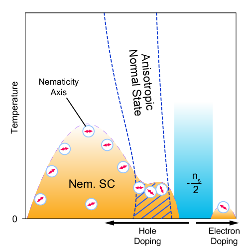
The various phases discussed throughout this article are summarized in Fig. 6. The fact that an anisotropic response to an in-plane magnetic field is seen only in the superconducting state, but not in the wedge-like feature, suggests that the origins of nematicity in the normal and superconducting states are likely different. This is also consistent with the fact that these two orders compete, as evident from the suppression of when the wedge-like feature intersects with the superconducting dome. However, since both phases break the same six-fold lattice rotational symmetry, the order parameters of these two phases can interact beyond mere competition, which may be responsible for the rapid change of the ellipse direction in the coexisting region of the phase diagram (see Supplementary Material 33). Moreover, normal-state nematic fluctuations may play an important role in favoring a superconducting ground state that is also nematic. While the onset of nematicity and of superconductivity seem very close in our experiment (see Supplementary Material), it is possible that the nematic order in magic-angle TBG persists even above , a phenomenon known as vestigial nematic order 12; 14; 43. Interestingly, in Fig. 3b, there is a region just above the superconducting dome with positive transverse voltage signal at and . This not only has opposite sign than the anisotropy of the wedge-like state, but it also disappears when superconductivity is suppressed (Fig. 3c). Thus, this feature might be explained by a vestigial nematic order that forms prior to the condensation of Cooper pairs.12; 14; 43. Scanning probe experiments are encouraged in the future to confirm this nematic phase above the superconducting transition.
In summary, our experiments extend the already rich phase diagram of magic-angle TBG to include a nematic superconducting state and an anisotropic normal state above the ‘underdoped’ part of the superconducting dome. The competition between them results in a reduction of and in a fast rotation of the nematic director of the superconducting state. Our results pioneer the study of competing/intertwined quantum phases in a highly tunable two-dimensional correlated platform, which in turn may shed more light onto the unconventional superconductivity in iron-based compounds, doped Bi2Se3 and other nematic superconductors.
Acknowledgements.
We acknowledge helpful discussions with P. A. Lee, S. Todadri, A. Vishwanath, A. Hristov, I. Fisher, J. Venderbos, and S. A. Kivelson.References
- (1) P. W. Anderson, More is Different. Science 177, 393-396 (1972).
- (2) Keimer, B., Kivelson, S. A., Norman, M. R., Uchida, S. & Zaanen, J. From quantum matter to high-temperature superconductivity in copper oxides. Nature 518, 179-186 (2015).
- (3) Sachdev, S., Colloquium: Order and quantum phase transitions in the cuprate superconductors, Rev. Mod. Phys. 75, 913 (2003).
- (4) E. Fradkin, S. A. Kivelson, M. J. Lawler, J. P. Eisenstein, A. P. Mackenzie, Nematic Fermi Fluids in Condensed Matter Physics. Ann. Rev. of Cond. Matt. Phys. 1, 153-178 (2010).
- (5) Fernandes, R. M., Chubukov, A. V., Schmalian, J., What drives nematic order in iron-based superconductors? Nat. Phys. 10, 97-104 (2014).
- (6) Rosenthal, E. P., Andrade, E. F., et. al. Visualization of electron nematicity and unidirectional antiferroic fluctuations at high temperatures in NaFeAs. Nat. Phys. 10, 225-232 (2014).
- (7) B. E. Feldman, et. al. Observation of a nematic quantum Hall liquid on the surface of bismuth. Science 354, 361 (2016).
- (8) V. Hinkov, D. Haug, et. al. Electronic Liquid Crystal State in the High-Temperature Superconductor YBa2Cu3O6.45. Science 319, 597-600 (2019).
- (9) J.-H. Chu, H.-H. Kuo, J. G. Analytis, I. R. Fisher, Divergent Nematic Susceptibility in an Iron Arsenide Superconductor. Science 337, 710-712 (2012).
- (10) Chuang, T.-M., Allan, M. P., et. al. Nematic Electronic Structure in the “Parent” State of the Iron-Based Superconductor Ca(Fe1–xCox)2As2. Science 327, 181-184 (2010).
- (11) Sato, Y., Kasahara, S., et. al. Thermodynamic evidence for a nematic phase transition at the onset of the pseudogap in YBa2Cu3Oy, Nature Phys. 13, 1074 (2017).
- (12) L. Nie, G. Tarjus, and S. A. Kivelson, Proc. National Acad. Sci. U.S. A. 111, 7980-7985 (2014).
- (13) Fradkin, E., Kivelson, S. A., Tranquada, J. M. Theory of intertwined orders in high temperature superconductors. Rev. Mod. Phys. 87, 457 (2015).
- (14) Fernandes, R. M., Orth, P. P. & Schmalian, J. Intertwined Vestigial Order in Quantum Materials: Nematicity and Beyond. Annu. Rev. Condens. Matter Phys. 10, 133-154, (2019).
- (15) Proust, C. and Taillefer, L., The Remarkable Underlying Ground States of Cuprate Superconductors, Ann. Rev. Cond. Matt. Phys. 10, 409-429 (2019).
- (16) Chang, J., Blackburn, E., et. al. Direct observation of competition between superconductivity and charge density wave order in YBa2Cu3O6.67, Nature Phys. 12, 871 (2012).
- (17) Edkins, S. D., Kostin, A., et. al. Magnetic field–induced pair density wave state in the cuprate vortex halo. Science 364, 976-980 (2019).
- (18) Li, J., Pereira, P. J., et. al. Nematic superconducting state in iron pnictide superconductors. Nat. Comm. 8, 1880 (2017).
- (19) Matano, K., Kriener, M., et. al. Spin-rotation symmetry breaking in the superconducting state of CuxBi2Se3. Nat. Phys. 12, 852-854 (2016).
- (20) Shen, J., He, W., et. al. Nematic topological superconducting phase in Nb-doped Bi2Se3. npj Quantum Mater. 2, 59 (2017).
- (21) Kuntsevich, A. Y., Bryzgalov, M. A., Structural distortion behind the nematic superconductivity in SrxBi2Se3. New J. Phys. 20, 103022 (2018).
- (22) Asaba, T., Lawson, B. J., et. al. Rotational Symmetry Breaking in a Trigonal Superconductor Nb-doped Bi2Se3. Phys. Rev. X 7, 011009 (2017).
- (23) Pan, Y., Nikitin, A. M., et. al. Rotational symmetry breaking in the topological superconductor SrxBi2Se3 probed by upper-critical field experiments. Sci. Rep. 6, 28632 (2016).
- (24) Smylie, M. P., Willa, K., et. al. Superconducting and normal-state anisotropy of the doped topological insulator Sr0.1Bi2Se3. Sci. Rep. 8, 7666 (2018).
- (25) Cao, Y., Fatemi, V., Demir, A., Fang, S., Tomarken, S. L., Luo, J. Y., Sanchez-Yamagishi, J. D., Watanabe, K., Taniguchi, T., Kaxiras, E. , Ashoori, R. & Jarillo-Herrero, P. Correlated Insulator Behaviour at Half-Filling in Magic Angle Graphene Superlattice. Nature 556, 80-84 (2018).
- (26) Cao, Y., Fatemi, V., Fang, S., Watanabe, K., Taniguchi, T., Kaxiras, E. & Jarillo-Herrero, P. Unconventional superconductivity in magic-angle graphene superlattices. Nature 556, 43-50 (2018).
- (27) Morell, E. S., Correa, J. D., Vargas, P., Pacheco, M. & Barticevic, Z. Flat bands in slightly twisted bilayer graphene: Tight-binding calculations. Phys. Rev. B 82, 121407 (2010).
- (28) Bistritzer, R. & MacDonald, A. H. Moiré bands in twisted double-layer graphene. Proc. Natl. Acad. Sci. U. S. A. 108(30), 12233-12237 (2011).
- (29) J. M. B. Lopes dos Santos, N. M. R. Peres, A. H. Castro Neto, Phys. Rev. B 86, 155449 (2012).
- (30) Yankowitz, M., Chen, S. et. al. Tuning superconductivity in twisted bilayer graphene. Science 363, 1059-1064 (2019).
- (31) Kim, K., Yankowitz, M., Fallahazad, B., Kang, S., Movva, H. C. P., Huang, S., Larentiz, S., Corbet, C. M., Taniguchi, T., Watanabe, K., Banerjee, S. K., LeRoy, B. J. & Tutuc, E. van der Waals Heterostructures with High Accuracy Rotational Alignment. Nano Lett. 16, 1989 (2016).
- (32) Cao, Y., Luo, J. Y., Fatemi, V., Fang, S., Sanchez-Yamagishi, J. D., Watanabe, K., Taniguchi, T., Kaxiras, E. & Jarillo-Herrero, P. Superlattice-induced insulating states and valley-protected orbits in twisted bilayer graphene. Phys. Rev. Lett. 117, 116804 (2016).
- (33) See online Supplementary Materials.
- (34) Lu, X., Stepanov, P., Yang, W., Xie, M., Aamir, M. A., Das, I., Urgell, C., Watanabe, K., Taniguchi, T. Zhang, G., Bachtold, A., MacDonald, A. H. & Efetov, D. K., Superconductors, Orbital Magnets, and Correlated States in Magic Angle Bilayer Graphene. Nature 574, 653–657(2019).
- (35) Ramshaw, B. J., Sabastian, S. E., McDonald, R. D., Day, J., Tan, B. S., Zhu, Z., Betts, J. B., Liang, R., Bonn, D. A., Hardy, W. N., Harrison, N., Quasiparticle mass enhancement approaching optimal doping in a high- superconductor. Science 348, 317-320 (2015).
- (36) Walmsley, P., Fisher, I. R., Determination of the resistivity anisotropy of orthorhombic materials via transverse resistivity measurements. Rev. Sci. Instruments 88, 043901 (2017).
- (37) Wu, J., Bollinger, A. T., He, X. & Boz̆ović, I., Nature 547, 432-435 (2017).
- (38) Isobe, H., Yuan, N. F. & Fu, L., Unconventional Superconductivity and Density Waves in Twisted Bilayer Graphene, Phys. Rev. X 8, 041041 (2018).
- (39) Kozii, V., Isobe, H., Venderbos, J. W. F., Fu, L., Nematic superconductivity stabilized by density wave fluctuations: Application to twisted bilayer graphene. arXiv:1810.04159 (2018).
- (40) Tinkham, M. Introduction to superconductivity (Courier Corporation, 1996).
- (41) R. M. Fernandes & J. W. F. Venderbos, Nematicity with a twist: rotational symmetry breaking in a moiré superlattice. arXiv:1911.11367 (2019).
- (42) Verderbos, J. W. F., Kozii, V., Fu, L., Identification of nematic superconductivity from the upper critical field. Phys. Rev. B 94, 094522 (2016).
- (43) Hecker, M. & Schmalian, J., Vestigial nematic order and superconductivity in the doped topological insulator Cux Bi2Se3, npj Quantum Materials 3, 26 (2018).
- (44) G. Li, A. Luican, J. M. B. Lopes dos Santos, A. H. Castro Neto, A. Reina, J. Kong, E. Y. Andrei, Nature Phys. 6, 109 (2010).
- (45) A. Luican, G. Li, A. Reina, J. Kong, R. R. Nair, K. S. Novoselov, A. K. Geim, E. Y. Andrei, Phys. Rev. Lett. 106, 126802 (2011).
- (46) Kerelsky, A., McGilly, L. J., Kennes, D. M., Xian, L., Yankowitz, M., Chen, S., Watanabe, K., Taniguchi, T., Hone, J., Dean, C., Rubio, A. & Pasupathy, A. N. Nature 572, 95-100 (2019).
- (47) Jiang, Y., Lai, X., Watanabe, K., Taniguchi, T., Haule, K., Mao, J. & Andrei E. Y. Nature 573, 91-95 (2019).
- (48) Li, S.-Y., Liu, K.-Q., Yin, L.-J., Wang, W.-X., Yan, W., Yang, X.-Q., Yang, J.-K., Liu H., Liang, H. & He, L. Phys. Rev. B 96, 155416 (2017).
- (49) Kang, J. and Vafek, O. Strong coupling phases of partially filled twisted bilayer graphene narrow bands. Phys. Rev. Lett. 122, 246401 (2019).
- (50) Dodaro, J. F, Kivelson, S. A., Schattner, Y., Sun, X. Q., and Wang, C., Phases of a phenomenological model of twisted bilayer graphene. Phys. Rev. B 98, 075154 (2018).
- (51) Chichinadze, D. V., Classen, L., Chubukov, A. V. Nematic superconductivity in twisted bilayer graphene. arXiv:1910.07379 (2019).
- (52) D. Blankschtein, Y. Shapir, and A. Aharony, Phys. Rev. B 29, 1263 (1984).