Two-dimensional topological insulator state in double HgTe quantum well
Abstract
The two-dimensional topological insulator phase has been observed previously in single HgTe-based quantum wells with inverted subband ordering. In double quantum wells (DQWs), coupling between the layers introduces additional degrees of freedom leading to a rich phase picture. By studying local and nonlocal resistance in HgTe-based DQWs, we observe both the gapless semimetal phase and the topological insulator phase, depending on parameters of the samples and according to theoretical predictions. Our work establishes the DQWs as a promising platform for realization of multilayer topological insulators.
Topological insulators (TIs) are a new class of materials characterized by an insulating band gap in the bulk, like in ordinary band insulators, but having topologically protected conducting states at their edges for two-dimensional (2D) TIs or at the surface for three-dimensional TIs Kane ; Bernevig ; Hasan ; Qi . The TI phase has been theoretically predicted Bernevig and experimentally realized in HgTe quantum wells (QWs) with CdxHg1-xTe barriers Konig . The crucial properties enabling the 2D TI states in these systems are the strong spin-orbit coupling that leads to inverted band structure of HgTe and the size quantization that opens the gaps in the electron spectrum of initially gapless HgTe. In HgTe-based QWs with the well width above the critical one, , the upper size-quantization subband of heavy holes stays above the electronlike subbands. This inverted subband ordering produces the 2D TI phase with one-dimensional edge states inside the gap in the bulk 2D subband spectrum. Electron transport in the edge states is expected to be highly ballistic because the elastic backscattering of electrons is forbidden due to the time reversal symmetry in the absence of magnetic field and magnetic impurities. Experimental manifestations of the edge transport are the quantization of conductance at the universal value and the appearance of nonlocal voltage away from the dissipative bulk current path Konig ; Roth .
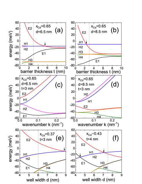
Double quantum wells (DQWs) are bilayer systems consisting of two QWs separated by a tunneling-transparent barrier. Theoretical studies suggest kristopenko that the picture of phase states in these structures is strongly affected compared to the single QW case and becomes more rich because of the additional degrees of freedom associated with an increase in the number of 2D subbands and tunnel-induced hybridization between them. In particular, the subband ordering depends not only on the well width and Cd content in the barriers but also on the barrier thickness , and is sensitive to the asymmetry induced, for example, by a transverse electric field. Figure 1 (a,b) shows a typical dependence of subband edges on at a fixed for symmetric HgTe-based wells (see suppl for the details of calculations). The electronlike subbands E1 and E2, formed as a result of coupling between the states and the light hole part of states, are characterized by the wave functions which strongly penetrate into the barriers and, therefore, show a significant tunnel-induced splitting. In contrast, the hole subbands H1-H4, originating from the heavy hole part of states, are characterized by the wave functions weakly penetrating into the barriers because of the large effective mass. Thus, the tunnel-induced splitting of the pairs of subbands H1-H2 and H3-H4 exists only at very small , while for nm their energies are the same as in the single QWs. The degeneracy of H1 and H2 subbands is lifted at nonzero wave vector , forming two branches with the opposite dispersion in the case of mixed ordering of subbands, E1-H2-H1-E2, which results in a gapless energy spectrum, Fig. 1 (c). With increasing and/or , a fully inverted ordering, E1-E2-H2-H1, is realized, and a gapped TI phase appears, Fig. 1 (d). The energy spectrum in the gapless phase resembles the bilayer graphene spectrum castro1 with the absence of valley degeneracy note .
Similar as in bilayer graphene castro2 , it is predicted that the gapless phase in symmetric HgTe DQWs can be transformed into a gapped phase by breaking the inversion symmetry of two wells via a transverse electric field due to asymmetric doping or external gate biasing michetti ; kristopenko . Since the gap energy depends on the field, both these systems are the tunable gap semiconductors. However, there is a principal difference between the biased bilayer graphene and asymmetric HgTe DQWs: in the latter case the topologically protected edge states appear in the gap. Indeed, in contrast to bilayer graphene, HgTe-based DQWs possess topological properties due to subband inversion, and the calculations based on the effective Hamiltonian models michetti ; kristopenko ; baum show coexistence of the bulk and edge states in the gapless semimetal phase. Thus, it is expected that opening the gap in HgTe DQWs by the field makes them 2D TIs, where the edge state transport can be detected experimentally.
In this Letter, we present the results of studies of the local and nonlocal resistance in HgTe-based DQWs. By studying several groups of samples with different parameters , , and , we have observed both the gapped phase and the gapless semimetal phase, clearly distinguished by the temperature dependence of the local resistance. By measuring nonlocal resistance in the gapped samples, we confirm the edge state transport in the absence of magnetic field, thereby providing the experimental evidence of the 2D TI phase in HgTe DQWs. Furthermore, we observe the gap and the edge state transport in the DQWs which are expected to be in the gapless phase if the transverse electric field were absent.
Double quantum wells HgTe/CdxHg1-xTe with [013] surface orientation and equal well widths from 6.0 to 8.5 nm were prepared by molecular beam epitaxy (MBE) suppl . The layer thicknesses were determined by ellipsometry during the MBE growth, with the accuracy nm. The devices are designed for multiterminal measurements and contain three 3.2 m wide consecutive segments of different length (2, 8, and 32 m) and 9 contacts (Fig. 2) shunting both QW layers. A dielectric layer, 200 nm of SiO2, was deposited on the sample surface and then covered by a TiAu gate. The density variation with the gate voltage was cm-2 V-1. The transport measurements were performed in the range of temperatures from 1.4 K to 70 K by using a standard four-point circuit with 1-13 Hz ac current of 1-10 nA through the sample, which is sufficiently low to avoid overheating effects. For each set of parameters, results for two typical devices (1,2) are represented. Table I lists parameters of the devices, including the gate voltage corresponding to the charge neutrality point (CNP) at K.
| (nm) | (nm) | (V) | properties | |
|---|---|---|---|---|
| 8.5 | 3 | 0.65 | -0.7 | TI |
| 7.5 | 4 | 0.43 | -0.8 | narrow-gap TI |
| 6.5 | 3 | 0.65 | -5 | gapless |
| 6.0 | 3 | 0.37 | -2.4 | TI |
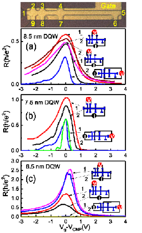
Figure 2 presents the local and nonlocal resistances at zero magnetic field for the samples fabricated from the structures with nm, nm, and nm. In the local configuration, the current flows between the contacts 1 and 5, and the voltage is measured between the short distance separated probes 2 and 3, , and between widely separated probes 3 and 4, . In the nonlocal configuration, the current flows between the contacts 2 and 9 while the voltage is measured between the probes 3 and 8, . A slower decrease of the resistances with in the negative voltage region is related to a larger density of states in the valence band.
We first focus on the results obtained in DQWs with nm and 7.5 nm. In the first one, the peaks of the resistances and are close to the quantity expected in the case of purely ballistic edge state transport in the multiprobe device shown in Fig. 2, though is larger than . In the second one, the peak resistance is considerably larger than . These observations contradict with the picture of ballistic edge state transport in 2D TIs implying that the backscattering is forbidden at sufficiently low temperatures Kane ; Bernevig ; Hasan ; Qi so the resistance is independent of the distance between the voltage probes. While some experimental works indeed confirm the quantized transport in multiprobe HgTe QW devices Roth ; Olshanetsky , the longest edge channel length that shows a quantized resistance peak never exceeds 10 m. We notice that the edge current in our experiment flows along the gated sample edge (see the top of Fig. 2), so the effective length of the edge channel segments between the probes and is longer than the geometrical distance (bulk current path) between these probes and is estimated as m and m suppl . Thus, the absence of ballisticity is expectable.
The lack of robustness of the ballistic edge state transport has attracted a lot of attention, and numerous explanations have been proposed in recent years maciejko . A detailed discussion of the existing theoretical models is beyond the scope of our paper. We emphasize that the edge state transport persists in both ballistic and diffusive regimes, while the values of local and nonlocal resistances depend on the sample design and measurement configurations. The most important characteristic feature of the 2D TIs, indicating the presence of the edge state transport, is the existence of nonlocal resistance of the order of resistance quantum Roth . We observe such nonlocal resistances in 8.5 nm and 7.5 nm DQWs. Figure 2 (a) and (b) shows a significant difference between and : the peaks of are narrower and this resistance disappears outside the bulk gap, where the edge channels are short circuited by the bulk conduction. Similar results were obtained for other nonlocal measurement configurations.
The Landauer-Büttiker formalism Buttiker allows one to find the resistance for any measurement configuration in multiprobe samples, by taking into account a finite probability of backscattering described by the mean free path length suppl :
| (1) |
Here, and (or and ) are the number of edge channel segments and their total length between the voltage (or current) leads along the arc that does not contain the current (or voltage) leads. Next, is the total number of segments, which is equal to the total number of leads, and is the total length of all segments, i.e., the perimeter of the sample. In the ballistic transport limit, , the resistance is an integer fraction of Roth ; Olshanetsky , while in the general case the resistance is sensitive to and is larger than the ballistic one. However, a comparison of Eq. (1) to the experimental peak resistances does not show a general agreement. The deviations are strong for the nonlocal configuration, where the ballistic limit corresponds to while the measured resistances are not larger than this value, as expected from Eq. (1) suppl , but, in fact, are considerably smaller. This means that the backscattering within the edge channel alone cannot explain the transport, and the other processes responsible for attenuation of the voltage signal, such as edge to bulk leakage of electrons and bulk current contribution, are important. Nevertheless, the very existence of nonlocal resistance is a sufficient proof for the domination of the edge transport near CNP in the samples with nm and nm, which also suggests the presence of the bulk gaps.
Now we turn to the observations for DQW structure with nm, Fig. 2 (c), which differs from the structure of Fig. 2 (a) only by the well width. One can see that the ratio is close to the ratio of the distances between the probes, which suggests the dominance of the bulk transport. More important, the nonlocal resistance is absent. This is the property associated with zero gap spectrum, shown in Fig. 1 (c) for this structure. Unlike the edge state conductivity in 8.5 nm and 7.5 nm DQWs, the conductivity in 6.5 nm devices is due to the bulk, while the edge contribution is short circuited.
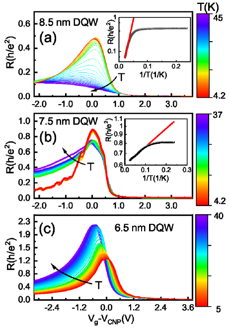
For a further proof of the different nature of the transport in the samples with open and closed bulk gap, we have measured the temperature dependence of the resistance near CNP. The variation of the resistance with the gate voltage and temperature is shown in Fig. 3. The evolution of the resistance in the samples with nm and nm resembles that for single well 2D TIs Gusev ; Olshanetsky . For 8.5 nm sample, the resistance decreases sharply at K while saturating below 15 K. For 7.5 nm sample, a decrease in the resistance with starts below 10 K, indicating a small mobility gap of 0.5-1 meV. Fitting the resistance dependence on by the activation law , we find the activation gap meV for 8.5 nm DQW and meV for 7.5 nm DQW. These values agree with calculated gap energies (see Fig. 1), taking into account the nm uncertainty in the knowledge of and . Below 10 K the conductance is saturated with temperature, demonstrating no significant temperature dependence, which also agrees with the resistance behavior in single well 2D TIs Gusev ; suppl . Therefore, the temperature dependence of the resistance in 8.5 nm and 7.5 nm DQWs justifies that the bulk gap exists so that the transport through the edge channels is expectable.
The DQWs with nm demonstrate the opposite temperature dependence: the resistance increases with increasing , indicating a metallic type of conductivity. A similar behavior is seen suppl in a single HgTe well with critical width , which is a gapless Dirac fermion system. With increasing , the resistance peak in Fig. 3 (c) shifts to the hole side and becomes wider. This behavior is related to asymmetry of the energy spectrum, and described within the bulk transport picture as follows. The bulk resistance reaches a maximum when the chemical potential stays in the point where the bands touch each other. As the density of states in the valence band is larger, for this position of the chemical potential the hole density is larger than the electron one, and the difference in the densities increases with . Thus, the gate voltage corresponding to the peak resistance is shifted away from the CNP to the hole side. In summary, the temperature dependence of the resistance in 6.5 nm DQWs justifies that the gap is closed and the transport occurs through the bulk.
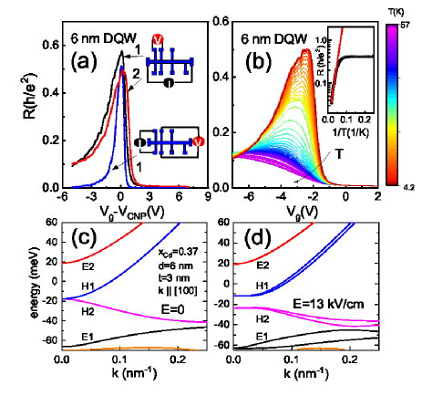
Finally, we present the results for DQWs with nm (Fig. 4), wich show a special behavior. According to our calculations [Fig. 1 (e) and Fig. 4 (c)], this structure is expected to be a gapless semimetal, while the transport measurements demonstrate that it is actually a 2D TI with the activation gap meV and a nonlocal response similar to those in Fig. 2 (a,b). This finding can be explained by the presence of an asymmetry, presumably related to specifics of MBE growth for this particular structure, for example, an uncontrollable chemical doping. Calculations of the energy spectrum of asymmetric DQWs confirm this assumption and show that the observed gap can be created by a transverse electric field kV/cm, which splits the heavy hole subbands H1 and H2 apart and also leads to Rashba spin splitting of all the subbands, Fig. 4 (d). While in bilayer graphene the transverse electric field can be controlled by double gates maher , fabrication of the devices with controllable gap based on MBE-grown HgTe DQWs requires numerous technological efforts. A forthcoming development of double gating technology for HgTe DQWs can open a possibility for electrical control of the edge state transport, which is important both for fundamental physics and for device applications.
In conclusion, we have demonstrated phase diversity in HgTe DQWs by observing both a topological insulator phase and a gapless semimetal phase that resembles the bilayer graphene. We have also detected a topological insulator phase whose existence requires the presence of a transverse asymmetry of DQWs, possibly produced by an internal electric field. We believe that our studies will be helpful for paving the way to the tunable topological insulators and the multilayer topological insulators.
The financial support of this work by RFBI Grant No. 18-02-00248a., FAPESP (Brazil), and CNPq (Brazil) is acknowledged.
References
- (1) C. L. Kane and E. J. Mele, Phys. Rev. Lett. 95, 146802 (2005); C. L. Kane and E. J. Mele, Phys. Rev. Lett. 95, 226801 (2005).
- (2) B. A. Bernevig and S. C. Zhang, Phys. Rev. Lett. 96, 106802 (2006); B. A. Bernevig, T. L. Hughes, and S. C. Zhang, Science 314, 1757 (2006).
- (3) M. Z. Hasan and C. L. Kane, Rev. Mod. Phys. 82, 3045 (2010); X-L. Qi and S.-C. Zhang, Rev. Mod. Phys. 83, 1057 (2011).
- (4) X.-L. Qi and S.-C. Zhang, Phys. Today 63, 33 (2010).
- (5) M. Konig, S. Wiedmann, C. Brune, A. Roth, H. Buhmann, L. W. Molenkamp, X.-L. Qi, and S.-C. Zhang, Science 318, 766 (2007).
- (6) A. Roth, C. Brune, H. Buhmann, L. W. Molenkamp, J.Maciejko, X.-L. Qi, and S.-C. Zhang, Science 325, 294 (2009).
- (7) S. S. Krishtopenko, W. Knap, and F. Teppe, Nat. Sci. Rep. 6, 30755 (2016).
- (8) P. Michetti, J. C. Budich, E. G. Novik, and P. Recher, Phys. Rev. B, 85, 125309 (2012); P. Michetti and B. Trauzettel, Appl. Phys. Lett. 102, 063503 (2013).
- (9) Supplemental Material, which includes Refs. [21-25].
- (10) A. H. Castro Neto, F. Guinea, N. M. R. Peres, K. S. Novoselov, and A. K. Geim, Rev. Mod. Phys. 81, 109 (2009).
- (11) A different kind of gapless semimetal can be created in a single HgTe QW by application of a strong in-plane magnetic field raichev ; gusev2 , in this case the spin degeneracy is missed as well.
- (12) O. E. Raichev, Phys. Rev. B 85, 045310 (2012).
- (13) G. M. Gusev, E. B. Olshanetsky, Z. D. Kvon, O. E. Raichev, N. N. Mikhailov, and S. A. Dvoretsky, Phys. Rev. B 88, 195305 (2013).
- (14) E. V. Castro, N. M. R. Peres, J. M. B. Lopes dos Santos, F. Guinea, and A. H. Castro Neto, J. Phys.: Conf. Ser. 129, 012002 (2008).
- (15) Y. Baum, T. Posske, I. C. Fulga, B. Trauzettel, and A. Stern, Phys. Rev. Lett. 114, 136801 (2015).
- (16) E. B. Olshanetsky, Z. D. Kvon, G. M. Gusev, A. D. Levin, O. E. Raichev, N. N. Mikhailov, and S. A. Dvoretsky, Phys. Rev. Lett., 114, 126802 (2015).
- (17) J. Maciejko, C. Liu, Y. Oreg, X.-L. Qi, C.Wu, and S.-C. Zhang, Phys. Rev. Lett. 102, 256803 (2009); Y. Tanaka, A. Furusaki, and K. A. Matveev, Phys. Rev. Lett. 106, 236402 (2011); V. Cheianov and L. I. Glazman, Phys. Rev. Lett. 110, 206803 (2013); A. Strom, H. Johannesson, and G. I. Japaridze, Phys. Rev. Lett. 104, 256804 (2010); N. Lezmy, Y. Oreg, and M. Berkooz, Phys. Rev. B 85, 235304 (2012); F. Crepin, J. C. Budich, F. Dolcini, P. Recher, and B. Trauzettel, Phys. Rev. B 86, 121106(R) (2012); J. I. Vayrynen, M. Goldstein, and L. I. Glazman, Phys. Rev. Lett. 110, 216402 (2013); A. M. Lunde and G. Platero, Phys. Rev. B 88, 115411 (2013); S. Essert, V. Krueckl, and K. Richter, Phys. Rev. B 92, 205306 (2015); P. P. Aseev and K. E. Nagaev, Phys. Rev. B 94, 045425 (2016); J. Wang, Y. Meir, and Y. Gefen, Phys. Rev. Lett. 118, 046801 (2017); P. Novelli, F. Taddei, A. K. Geim, and M. Polini, Phys. Rev. Lett. 122, 016601 (2019).
- (18) M. Büttiker, Phys. Rev. B 38, 9375 (1988).
- (19) G. M. Gusev, E. B. Olshanetsky, Z. D. Kvon, N. N. Mikhailov and S. A. Dvoretsky, Phys. Rev. B 87, 081311(R) (2013).
- (20) P. Maher, L. Wang, Y. Gao, C. Forsythe, T. Taniguchi, K. Watanabe, D. Abanin, Z. Papi, P. Cadden-Zimansky, J. Hone, P. Kim, and C. R. Dean, Science 345, 61 (2014).
- (21) Z. D. Kvon, E. B. Olshanetsky, D. A. Kozlov, N. N. Mikhailov, S. A. Dvoretskii, JETP Lett. 87, 502 (2008).
- (22) B. Büttner, C. X. Liu, G. Tkachov, E. G. Novik, C. Brüne, H. Buhmann, E. M. Hankiewicz, P. Recher, B. Trauzettel, S. C. Zhang, and L. W. Molenkamp, Nat. Phys. 7, 418 (2011).
- (23) D. A. Kozlov, Z. D. Kvon, N. N. Mikhailov, and S. A. Dvoretskii, JETP Lett. 96, 730 (2012).
- (24) E. G. Novik, A. Pfeuffer-Jeschke, T. Jungwirth, V. Latussek, C. R. Becker, G. Landwehr, H. Buhmann, and L. W. Molenkamp, Phys. Rev. B 72, 035321 (2005).
- (25) C. Brüne, C. X. Liu, E. G. Novik, E. M. Hankiewicz, H. Buhmann, Y. L. Chen, X. L. Qi, Z. X. Shen, S. C. Zhang, and L. W. Molenkamp, Phys. Rev. Lett. 106, 126803 (2011).
I Supplementary material:Two-dimensional topological insulator state in double HgTe quantum well
II Sample description and magnetotransport measurements
In the main text, we describe the experimental results for double quantum well (DQW) samples in zero magnetic field. The structures containing HgTe quantum well layers placed between CdxHg1-xTe barriers with surface orientation [013] studied here were grown by molecular beam epitaxy (MBE). A schematic view of the layer structure for the samples with 6.5 nm well width is presented in Fig. 1 (a). As shown in the previous publications kvon1 , the use of substrates inclined to the singular orientations may lead to growth of more perfect films. Therefore, the efficient growth of alloys is done predominantly on the substrates with surface orientations of [013], which deviate from the singular orientation by approximately . To prepare the gate, a dielectric layer containing 200 nm SiO2 was first grown on the structure using the plasmochemical method. Then, the TiAu gate was deposited.
Fabrication of ohmic contact to HgTe quantum well is similar to that for other 2D systems, such as GaAs quantum wells: the contacts were formed by the burning of indium directly to the surface of large contact pads. Modulation-doped HgTe/CdHgTe quantum wells are typically grown at 180o C. Therefore, in contrast to III-V compounds, the temperatures during the contact fabrication process are relatively low. On each contact pad, the indium diffuses vertically down, providing ohmic contact to both quantum wells, with the contact resistance in the range of 10-50 kOhm. During the AC measurements we always control Y-component of the impedance that never excess 5% of the total impedance, which demonstrates good ohmicity of the contacts.
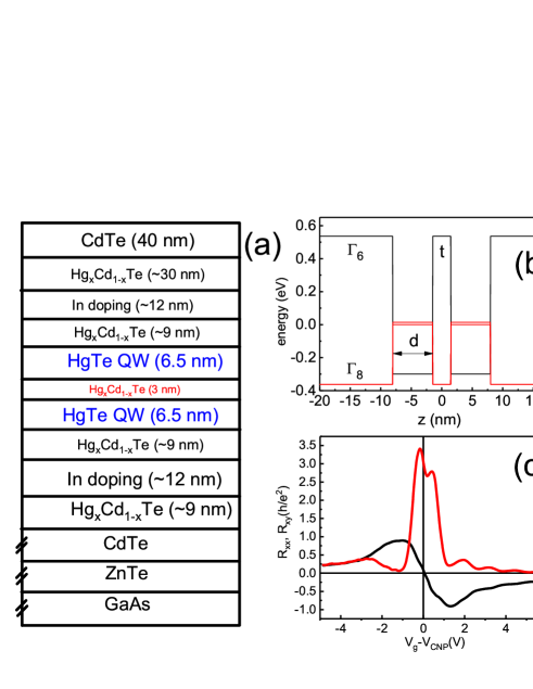
Low-temperature magnetotransport measurements were carried out to identify the charge neutrality point (CNP) and to obtain a relation between the induced carrier density and the gate voltage . By sweeping the gate voltage, we have found a continuous crossover from electron to hole type of conductivity, when the Fermi level is shifted from the conduction to the valence band. The possibility to tune the carrier density electrostatically enables the observation of electron and hole transport in a single device, making it possible to control filling of Landau levels in the presence of a perpendicular magnetic field. Figure 1 (c) shows the longitudinal and Hall resistances, and , as functions of the gate voltage at a fixed magnetic field T. The plateaux with , accompanied by the minima in , are clearly seen for electrons with filling factor from to . As is swept through the CNP, the longitudinal resistivity shows a maximum, whereas goes gradually through zero from negative on the electron side to positive on the hole side. It is a clear indication of CNP position and electron-hole crossover as a function of the gate voltage. From the resistance minima, we obtain the density variation with gate voltage cm-2V-1, which coincides with the density variation extracted from the capacitance measurements.
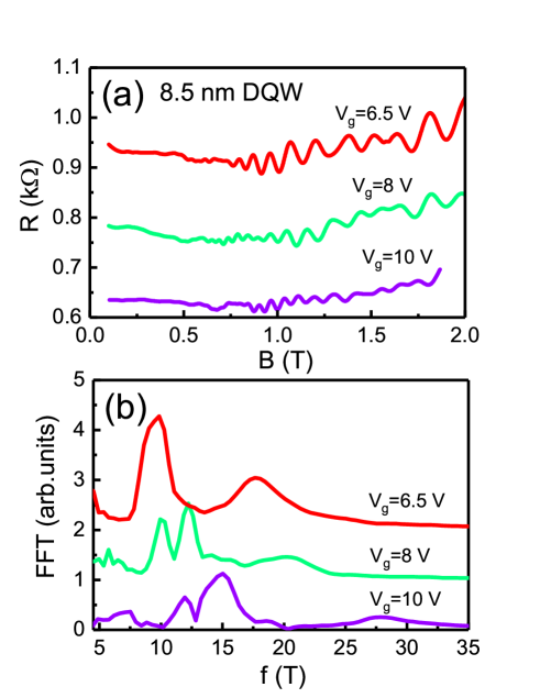
The Shubnikov-de Haas oscillations was measured for all DQWs in the region of electron conductivity. The magnetoresistance shows two sets of oscillations corresponding to two branches of conduction-band carriers. An example of such oscillations is given in Fig. 2.
In the quantum Hall regime, the bilayer system has a rich phase diagram in comparison with a single well. We performed transport measurements in HgTe DQWs and observed numerous crossings between Landau levels for both gapless and gapped samples, the results will be reported elsewhere.
III Transport measurements in single quantum wells
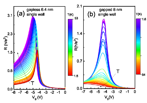
The 2D topological insulator (TI) phase state has been observed previously in single HgTe/CdxHg1-xTe quantum wells in the inverted band regime, when the well width is larger than the critical width, Kane ; Bernevig . For , one has nm, depending on the surface orientation and strain. When , the band gap collapses, and the energy spectrum corresponds to gapless single cone Dirac fermions (DF). In HgTe-based DQWs, modification of the spectrum depends also on the tunneling barrier thickness and height, as has been mentioned in the main text. It is useful to compare transport results obtained in double well and single well structures. The temperature dependence of the resistance in DQWs for both gapless and gapped samples has been shown in the main text. In Fig. 2 we show the variation of the resistance with gate voltage and temperature for single quantum well with nm, which is expected to be a gapless DF system buttner ; kvon , and for single quantum well with nm, which is a 2D TI Konig ; Gusev . For these two samples, the temperature behavior is opposite: the resistance increases in the DF system and decreases in the TI. For K, the temperature dependence of the resistance in TI fits very well the activation law , where is the activation (mobility) gap. The thermally activated behavior corresponds to a gap of 15 meV between the conduction and valence bands in the HgTe well. For K, the resistance is saturated with temperature, demonstrating no significant temperature dependence. In the DF system, the shift of the resistance peak with temperature is most likely related to electron-hole asymmetry, as in the case of gapless DQWs. In summary, the dependence of the resistance on temperature and gate voltage in the gapped and gapless single quantum wells is similar to that observed in the gapped and gapless DQWs.
IV Calculations of energy spectrum
The numerical calculations of electron energy spectrum are based on the Kane Hamiltonian whose description with applications for different orientations of the heterointerface is given in Ref. raichev . The energy is counted from the heavy hole band edge in HgTe. The relative positions of the band edges of in HgTe, in CdTe, and in CdTe are eV, eV, and eV, respectively. The energy separation between and bands is 1.0 eV for both HgTe and the barrier region. The Kane matrix element and the Luttinger parameters , , and for HgTe and CdTe are taken from Ref. novik . Also, a strain-induced shift meV of light hole band with respect to heavy hole band in HgTe layer on CdTe substrate brune has been taken into account. For structures with CdxHg1-xTe barriers, the band edge energies and Luttinger parameters in the barriers, as well as the strain-induced shift in HgTe, have been obtained by a linear interpolation with respect to Cd content . The Schroedinger equation for columnar wave function is a matrix differential equation of the second order with one independent variable, the growth axis coordinate . To describe asymmetrical structures, the -dependent steplike band energy profile [Fig. 1 (b)] was modified by adding the electrostatic potential energy . After discretization along , the differential equation is transformed to a finite-difference equation, which is solved by using the Thomas algorithm generalized for the case of matrix coefficients.
The influence of the interface orientation on the band structure of DQWs is similar to that for single well systems raichev . Compared to [001]-grown structures, the [013]-grown DQWs show shifts of the 2D subbands by several meV and modification of their dispersion, and also a hybridization of electronlike subbands with some heavy hole subbands even at zero , as seen in Fig. 1 (e) and (f) of the main text.
V Resistance of multiprobe 2D TI device with edge backscattering
To derive Eq. (1) of the main text, the edge channels encircling the perimeter of the 2D TI sample are represented by an equivalent circuit of resistors in series, each individual resistor corresponds to a segment between an adjacent pair of leads with the two-terminal resistance , where is the length of the segment. Applying the Kirchhoffs rules, one obtains Eq. (1), where is the voltage measured between the leads and while the current is maintained between the leads and .
The effective lengths of the edge channel segments in the device shown in the top of Fig. 2 of the main text are estimated as , , , , , , , , and (all the length are in m). The estimates are obtained by adding the lengths of vertical line segments under the gate (approximately, the top part adds 2 m and the bottom part adds 4 m) to the geometrical lengths between the contacts.
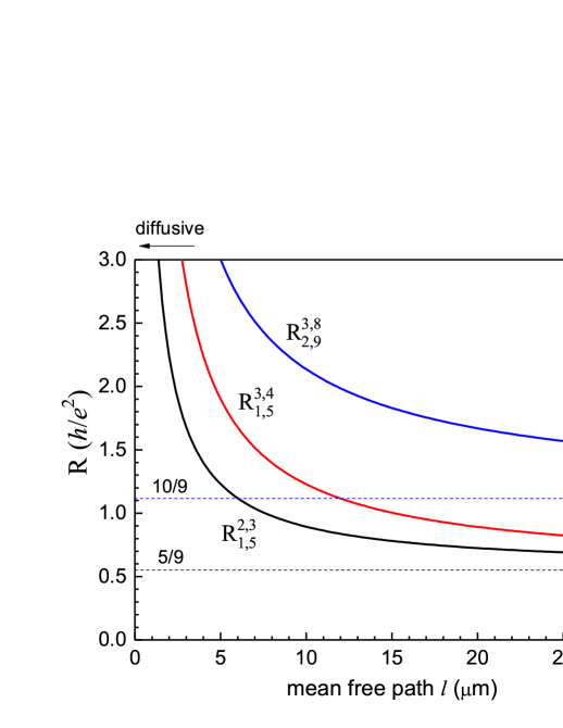
Applying Eq. (1) of the main text, one can plot the dependence of multiprobe resistances on the mean free path length . The results are shown in Fig. 4. Whereas the theoretical model explains the observed inequality in the local configurations, the calculated nonlocal resistances appear to be considerably larger than the observed ones. Therefore, accounting for the backscattering within the edge channels is insufficient for explanation of the observed resistances in the 2D TI HgTe-based systems. On the other hand, a dramatic suppression of nonlocal resistances can occur due to leakage of electrons from the edge channel to the 2D bulk ”puddles” placed nearby the edge and also due to partial short circuiting of the edge transport by the bulk currents. Both of these processes are expected to be important in our gapped samples because of small values of the gap energies.
References
- (1) Z. D. Kvon, E. B. Olshanetsky, D. A. Kozlov, N. N. Mikhailov, S. A. Dvoretskii, JETP Lett. 87, 502 (2008).
- (2) C. L. Kane and E. J. Mele, Phys. Rev. Lett. 95, 146802 (2005); C. L. Kane and E. J. Mele, Phys. Rev. Lett. 95, 226801 (2005).
- (3) B. A. Bernevig and S. C. Zhang, Phys. Rev. Lett. 96, 106802 (2006); B. A. Bernevig, T. L. Hughes, and S. C. Zhang, Science 314, 1757 (2006).
- (4) B. Büttner, C. X. Liu, G. Tkachov, E. G. Novik, C. Brüne, H. Buhmann, E. M. Hankiewicz, P. Recher, B. Trauzettel, S. C. Zhang, and L. W. Molenkamp, Nat. Phys.7, 418 (2011).
- (5) D. A. Kozlov, Z. D. Kvon, N. N. Mikhailov, and S. A. Dvoretskii, JETP Lett. 96, 730 (2012).
- (6) M. Konig, S. Wiedmann, C. Brüne, A. Roth, H. Buhmann, L. W. Molenkamp, X.-L. Qi, and S.-C. Zhang, Science 318, 766 (2007).
- (7) G. M. Gusev, E. B. Olshanetsky, Z. D. Kvon, N. N. Mikhailov and S. A. Dvoretsky, Phys. Rev. B, 87, 081311(R) (2013).
- (8) O. E. Raichev, Phys. Rev. B 85, 045310 (2012).
- (9) E. G. Novik, A. Pfeuffer-Jeschke, T. Jungwirth, V. Latussek, C. R. Becker, G. Landwehr, H. Buhmann, and L. W. Molenkamp, Phys. Rev. B 72, 035321 (2005).
- (10) C. Brüne, C. X. Liu, E. G. Novik, E. M. Hankiewicz, H. Buhmann, Y. L. Chen, X. L. Qi, Z. X. Shen, S. C. Zhang, and L. W. Molenkamp, Phys. Rev. Lett. 106, 126803 (2011).