Optically enhanced electric field sensing using nitrogen-vacancy ensembles
Abstract
Nitrogen-vacancy (NV) centers in diamond have shown promise as inherently localized electric-field sensors, capable of detecting individual charges with nanometer resolution. Working with NV ensembles, we demonstrate that a detailed understanding of the internal electric field environment enables enhanced sensitivity in the detection of external electric fields. We follow this logic along two complementary paths. First, using excitation tuned near the NV’s zero-phonon line, we perform optically detected magnetic resonance (ODMR) spectroscopy at cryogenic temperatures in order to precisely measure the NV center’s excited-state susceptibility to electric fields. In doing so, we demonstrate that the characteristically observed contrast inversion arises from an interplay between spin-selective optical pumping and the NV centers’ local charge distribution. Second, motivated by this understanding, we propose and analyze a method for optically-enhanced electric-field sensing using NV ensembles; we estimate that our approach should enable order of magnitude improvements in the DC electric-field sensitivity.
I Introduction
The precision measurement of electric fields remains an outstanding challenge at the interface of fundamental and applied sciences [1, 2, 3, 4, 5]. Leading electric field sensors are often based upon nanoelectronic systems [6, 7, 8, 9], electromechanical resonators [10, 11], or Rydberg-atom spectroscopy [12, 13, 14]. While such techniques offer exquisite sensitivities, their versatility can be limited by intensive fabrication, calibration or operation requirements.
More recently, quantum sensors based on solid-state spin defects have emerged as localized probes [15, 16, 17, 18], offering nanoscale spatial resolution and the ability to operate under a wide variety of external conditions [19, 20, 21, 22, 23, 24, 25, 26]. The spin sub-levels of such defects are naturally coupled to magnetic fields [17, 24, 27], but exhibit comparatively weak susceptibilities to electric fields [28]. To this end, a tremendous amount of effort has focused on developing techniques to improve spin-defect-based electrometry [16, 29, 30, 31, 32, 33, 34, 35, 36, 37].
Broadly speaking, these efforts can be divided into two categories: (i) leveraging orbital states (as opposed to spin states), which exhibit significantly stronger coupling to electric fields, or (ii) utilizing high-density ensembles, which enhances the sensitivity as , the standard quantum limit [38]. Each of these approaches, however, faces its own obstacles. In the first case, accurate measurements of the electronic susceptibilities have proven challenging due to the deleterious effects of local charge traps observed in single defect experiments [39, 40, 41, 42, 43, 44, 45, 46, 37, 47]. In the latter case, higher densities exacerbate inhomogeneous broadening, which can ultimately overwhelm any statistical improvement in sensitivity.
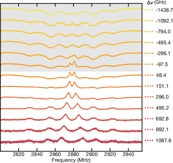
In this paper, we propose and analyze a technique, inspired by atomic saturation spectroscopy, designed to mitigate these challenges [48, 49, 49]. In particular, we focus on dense ensembles of nitrogen vacancy (NV) color centers in diamond—a spin defect which can be optically polarized and coherently manipulated via microwave fields [50, 26]. The essence of our approach is to apply resonant optical excitation to polarize a subgroup of an inhomogeneously broadened ensemble, and to probe the ground-state properties of this subgroup using optically detected magnetic resonance (ODMR). In doing so, we observe an unusual spectral feature — inverted-contrast peaks [51, 52] — which are significantly narrower than the magnetic spectra obtained via conventional, off-resonant ODMR (Fig. 1); crucially, this feature reveals an underlying correlation between the excited- and ground-state energy levels, which arises from the presence of internal electric fields within the diamond lattice [53, 54, 55].
Investigating these correlations yields three main results. First, we develop a microscopic model for the charge-induced, electric field environment that quantitatively reproduces all features of the resonant ODMR spectra [Fig. 1(a)]. Second, we demonstrate the first zero-field, ensemble-based method to determine the NV’s excited-state susceptibilities, yielding the transverse and longitudinal susceptibilities as and , respectively. Third, based on our microscopic insights, we propose and analyze an electrometry protocol that combines resonant optical excitation [52] with the excited-state’s strong electric-field susceptibility to enable a significant improvement in expected sensitivity. In particular, at low temperatures () we estimate a DC sensitivity of , representing a two order of magnitude improvement compared to the best known NV methods [29, 56].
II Inverted ODMR contrast
II.1 Overview
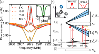
The NV center hosts an electronic spin-triplet ground state, where, in the absence of perturbations, the sublevels are degenerate and sit GHz above the state [Fig. 1(b)]. In high-density NV ensembles, this degeneracy is lifted most strongly by the local charge environment which directly couples the sublevels; this leads to typical ground-state ODMR spectra which exhibit a pair of heavy-tailed resonances centered around [inset, Fig. 1(a)] [53, 58].
Such ODMR spectra are usually obtained using continuous-wave off-resonant optical excitation, in which the NV center is initialized and read out with laser frequency detuned far above the zero-phonon line (ZPL), [Fig. 1(b)]. During such off-resonant excitation, the states fluoresce less brightly than the state. Moreover, in the absence of microwave excitation, the NV population accumulates in the state, owing to the spin-selective branching ratio of the singlet-decay channel. Applying resonant microwave excitation thus drives the population from the (brighter) state to the (dimmer) states. This leads to the typically observed negative-contrast ODMR feature [inset, Fig. 1(a)]. We note that for off-resonant driving, identical spectra are observed at both room temperature and cryogenic conditions [inset, Fig. 1(a)].
In contrast, continuous-wave ODMR spectra taken with an optical drive near resonance with the ZPL exhibit a marked temperature dependence characterized by two principal features [Fig. 1(a)]. Most prominently, for temperatures , the resonances invert, becoming a pair of narrow, positive-contrast peaks [51]. The entire spectrum, however, does not invert: Rather, these sharp peaks sit inside a broad envelope of negative contrast which is relatively temperature independent.
To understand the coexistence of these features, one must consider the interplay between resonant optical pumping and the local charge environment [51, 53]. Under resonant optical excitation, only one of the ground-state sublevels is driven to the excited state [Fig. 1(b)], while the other sublevels are optically dark and hence accumulate population. Microwave excitation drives population back into the resonant sublevel, leading to an increase in flourescence — i.e. a positive-contrast ODMR feature [Fig. 2(a)]. This resonant pumping mechanism is highly dependent on temperature: it can only occur if the thermally-broadened optical transition linewidth is smaller than , a situation that arises for [57].
The above picture is complicated by the presence of internal electric fields, which perturb the NV’s excited-state energy levels, leading to a distribution of optical resonance conditions within the NV ensemble. In particular, perpendicular electric fields (relative to the NV axis) split both the excited-state manifold and the ground-state sublevels [Fig. 1(b)] [59]. Crucially, this correlates the optical resonance condition and the ground-state splitting. Indeed, for relatively small optical detunings (Fig. 1), the resonance condition is generally satisfied by NVs subject to weak local electric fields; hence, the positive-contrast feature is relatively sharp and narrowly split. Meanwhile, the off-resonant pumping mechanism is more likely for NVs subject to large electric fields, resulting in a broad, negative-contrast background [Fig. 1(a)]. It is the superposition of these two features that gives rise to the unusual lineshapes observed in Fig. 1(a).
II.2 Microscopic model
Let us now turn our heuristic understanding into a quantitative microscopic model which takes into account: () the electric field distribution, () the excited state resonance condition, and () the ODMR lineshape for individual NV centers under resonant and off-resonant conditions.
To begin, we consider the internal electric field distribution arising from randomly placed elementary charges at an overall density . Physically, we expect these charges to consist primarily of the NV centers themselves (which are electron acceptors) and their corresponding donors — hence, , where is the NV defect density [53]. As the angular distribution of is fully symmetric, it suffices to consider the distribution for the electric field strength, . In Appendix C, we demonstrate via Monte Carlo simulations that this distribution may be approximated by the analytic expression,
| (1) |
Here, is a dimensionless electric field, where is approximately the electric field strength of the nearest charge, is the vacuum permittivity, and is the relative permittivity of diamond, which we take to be 5.7 [60].
Second, we consider the optical resonance condition given by the energy levels of the 3E excited state. In particular, we assume that electric fields, which couple directly to the orbital degree of freedom, dominate over hyperfine effects, including spin-orbit coupling and spin-spin interactions (see Appendix G) [61]. It is thus sufficient to model the excited state as two branches (upper and lower) of states, whose energies relative to are given by [61, 62]
| (2) |
Note that in our notation positive detuning is below the ZPL. The resonance condition for a given NV center optically excited with a laser detuning is then given by the function,
| (3) | ||||
| (4) |
where is the single-NV linewidth of the optical transition and is the Heaviside step function. In particular, is 1 on resonance and 0 otherwise.
Finally, we model the ground-state ODMR of each single NV using a primitive lineshape. This lineshape, denoted , is parameterized by the perpendicular electric field , which determines the splitting between the sublevels. It also incorporates two forms of broadening: () magnetic broadening arising from nearby spins (e.g. nitrogen defects and nuclear spins), and () non-magnetic broadening, which includes microwave power broadening and strain. The explicit form of is provided in Appendix C.
Putting all this together, we now determine the ensemble resonant ODMR. This consists of two separate contributions. The first is due to resonantly driven NVs and is given by integrating over primitive lineshapes whose associated electric field matches resonance condition:
| (5) |
where . An analogous expression (see Appendix C) describes the contribution due to off-resonantly driven NV centers. Adding these two cases together with a relative contrast factor, , yields the full spectrum:
| (6) |
The sign of determines whether the resonantly driven NV centers exhibit positive or negative contrast, while its magnitude depends on the details of the resonant optical pumping mechanism.
Using the above model, we perform numerical simulations of both resonant and off-resonant ODMR spectra for a range of temperatures. While our simulations depend on several input parameters, the most physically relevant of these are constrained by independent analysis. In particular, we determine the charge density ppm by fitting the off-resonant ODMR spectra to our charge-based model [inset, Fig. 1(a)] [53]; this suggests an NV density of ppm, which is consistent with prior density estimates for this sample [63]. In addition, as we discuss at length in the following section, we determine the excited state electric-field susceptibilities from independent measurements of resonant ODMR as function of optical detuning. The remaining temperature-dependent fit parameters, related to linewidth broadening and relative ODMR contrast, are provided in Appendix F.
The resulting lineshapes shown in Fig. 1(a) are in excellent agreement with the experimental data across all temperatures. Notably, even at high temperatures where the striking positive-contrast peak is absent, the resonant experimental spectra remain qualitatively distinct from the off-resonant spectra, yet are correctly captured by our lineshape simulations.
III Excited State Electric-field Susceptibilities
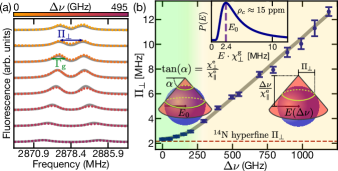
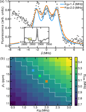
Interestingly, the correlation between the positive-contrast peaks and the optical resonance condition inspires a means of determining the excited-state electric-field susceptibilities from ground-state ODMR spectroscopy. In particular, as shown in Fig. 2(a), we perform ODMR measurements of the inverted-contrast feature as a function of the optical detuning. By tracking how the splitting, , of the positive-contrast feature changes as a function of , we fully determine the excited-state susceptibilities, and [Fig. 2(b)]. At its core, this ability to independently extract the susceptibilities stems from the fact that Fig. 2(b) exhibits two distinct regimes: at small detunings, exhibits a suppressed dependence on , while at large detunings, exhibits a linear dependence.
Let us now explain the origin of these two regimes. The splitting, , of the positive-contrast ODMR feature is controlled by: (i) the optical resonance condition and (ii) the distribution of electric fields. We focus on resonance with the lower branch, which is dominant resonant pumping mechanism for optical detunings below the ZPL (see Appendix B). This resonance condition (equation (2)) can be rearranged to obtain
| (7) |
which defines a “resonant cone” in electric field space with apex at [Fig. 2(b)]. On the other hand, the electric-field distribution is spherically symmetric and peaked at a characteristic electric field, , set by [inset, Fig. 2(b)].
For a given detuning, this provides a geometric interpretation for determining the electric field configurations most likely to match the resonance condition; in particular, these configurations are set by the highest-probability sphere that intersects the resonant cone [yellow circles in Fig. 2(b)]. At small detunings, this sphere is always at radius , implying that can only weakly depend on the detuning [64]. At large detunings, the sphere of radius no longer intersects the cone, and instead, the highest-probability intersecting sphere is the inscribed sphere [Fig. 2(b)]. The size of the inscribed sphere grows linearly with the detuning, and thus so does .
As a result of these two regimes, in Fig. 2(b) has both a slope, , and an elbow, at . From this information alone, we can analytically estimate and . In particular, setting be the exterior angle of the resonant cone, we obtain
| (8) | ||||
| (9) |
We estimate and from Fig. 2(b) and from the off-resonant spectra [Fig. 1(b), inset]. This yields and .
To refine these estimates and corroborate our geometric interpretation, we simulate the full resonant ODMR lineshape as a function of optical detuning and fit the simulated to the experimental data. Unlike the analytic estimates above, this model takes into account all resonant electric-field configurations. To perform the fits, we fix all parameters of our microscopic model except for the susceptibilities (see Appendix D for details). The best-fit susceptibilties are given by and [gray line in Fig. 2(b)], which agree within error bars with the analytic estimates.
These results represent a refinement over previous measurements of the excited state susceptibilities via single NV Starks shifts, which are strongly distorted by photo-ionized charge traps [39, 40, 41]. In contrast, ensemble measurements appear to be insensitive to the effects of charge traps [28, 29, 30]; indeed, assuming their positions are random, charge traps would contribute to the effective charge density but would not systematically bias the ensemble Stark shift [65].
Beyond allowing us to extract the susceptibilities, our numerical model fully reproduces the detuning-dependent experimental data [Fig. 2(a)]. In particular, the model quantitatively recovers two characteristic features of these spectra: a decrease in the overall fluorescence and an increase in the linewidth , for increasing . Physically, fluorescence declines with because the larger electric fields required for resonance are less likely. The dependence of on is more subtle and is discussed in Appendix E.
IV Optically Enhanced Electrometry
Our understanding of the interplay between internal electric fields and resonant excitation suggests a protocol for DC electric field sensing using NV ensembles. The protocol is premised on the fact that an external electric field parallel to the NV axis induces an overall shift of the excited-state levels. In effect, this is equivalent to changing the optical detuning, which we have already observed has two primary consequences: (i) it alters the splitting of the inverted-contrast peaks [Fig. 3(c)], and (ii) it changes the density of resonant configurations and therefore the overall fluorescence [Fig. 3(b)] 111Interestingly, the first of these effects has also been explored in the context of a complementary MW-free magnetometry protocol [52].
To leverage these effects for electrometry, we propose the following protocol. First, apply a bias electric field parallel to one of the NV orientations to spectrally isolate its excited state [73]. Second, perform resonant ODMR with fixed laser detuning below the peak of the ZPL such that positive-contrast peaks are clearly observed. Because overall fluorescence decreases with detuning, the optimal choice is the smallest detuning such that the positive contrast peaks disperse linearly with an applied field [see Appendix G, Fig 9(a)]. Finally, monitor the fluorescence at a fixed microwave drive frequency that maximizes the slope of the inner edge of one of the resonant ODMR peaks. Unless otherwise stated, we assume operating temperatures of throughout our discussion, as required for the occurrence of positive-contrast peaks.
Unlike typical NV electric field sensing methods, our protocol is sensitive to fields parallel to the NV axis and insensitive to perpendicular fields. Intuitively, the insensitivity to perpendicular fields owes to the random orientation of internal electric fields. To illustrate this, consider the level shift induced by a small perpendicular field oriented in the direction and assume internal perpendicular fields are randomly oriented in the plane with strength . The ensemble-average level shift, , of the lower branch is then given by
| (10) | ||||
| (11) |
which vanishes at leading order in .
We now evaluate the sensitivity of our protocol to parallel fields. We first estimate the sensitivity owing to the peak shift alone [17]:
| (12) |
where is the linewidth of the positive-contrast peak, is a numerical factor associated with the lorentzian lineshape, is the inherent ODMR contrast, is the total photon count rate, and is the ratio of resonant fluorescence to total fluorescence. Note that is an effective susceptibility (right inset, Fig. 3) related to the slope of with respect to [Fig. 2(b)]. Similarly, we estimate the sensitivity due to overall fluorescence variation:
| (13) |
where is the linewidth of the optical transition and is a numerical lineshape factor determined from experimental data (see Appendix G). The change in fluorescence due to both these mechanisms may be combined, leading to an overall sensitivity: (see Appendix G).
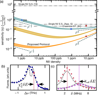
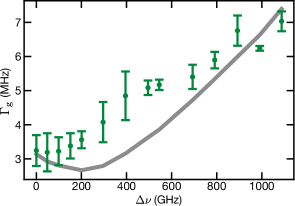
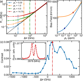
For our current sample, one finds a sensitivity, , assuming an illumination volume of [29]. This represents a improvement over established NV electrometry techniques (Fig. 3). The enhancement in sensitivity derives primarily from three factors: (i) a larger photon count rate due to resonant scattering, (ii) an improvement in contrast, and (iii) the ability to constructively combine the signal from peak-shifting and fluorescence variation.
The sensitivity of our protocol can be further improved by optimizing the NV density. As in our numerical model, let us assume that the total charge density is twice the NV density. At low densities, and are limited by the intrinsic broadening of resonant ODMR and the optical transition, respectively. By increasing density, both sensitivities improve according to the standard quantum limit, — the usual motivation for performing ensemble sensing (Fig. 3). However, at sufficiently high densities, the broadening due to internal electric fields becomes larger than the intrinsic broadening and the sensitivity degrades (Fig. 3) [74]; intuitively, this occurs because the NV ensemble is primarily sensing electric fields within the diamond lattice rather than the external signal. In particular, we show in Appendix G that the sensitivity degrades upon increasing density as (Fig. 3). Conversely, the sensitivity improves rapidly upon decreasing density until one reaches the crossover density between the intrinsically-broadened and charge-broadened regimes.
Interestingly, this crossover density is naturally different for and . In particular, the non-charge-induced broadening of the ground-state ODMR linewidth is often limited to by the 13C nuclear spin bath (although isotopically purified samples can exhibit narrower linewidths, changing the crossover density; this is discussed in more detail in Appendix G) [75, 76, 70]. This implies that is optimal at NV densities of ppb. On the other hand, these same magnetic fields only weakly affect the excited state. Rather, the non-charge-induced broadening of the excited-state, whose origin is less well understood, has been empirically observed to be [77, 78, 79]. This yields an optimal NV density for of ppb.
Putting everything together, we obtain an optimal total sensitivity of at an NV density ppb (Fig. 3, Table 2). This represents a two order of magnitude enhancement compared state-of-the-art NV methods (though these do not require cryogenic temperatures [29, 56]).
A few remarks are in order. First, while our sensitivity estimates assume an optically-thin sample, comparable sensitivities may be achieved at larger optical depths by monitoring, for example, transmission amplitude instead of fluorescence [78]. Second, monitoring resonant fluorescence variation alone via resonant excitation — without performing ODMR — already provides a significant electric field sensitivity, yielding a microwave-free version of our protocol. Since this microwave-free protocol does not require one to track the positive-contrast ODMR feature, it can also be applied at room temperature [Fig. 1(a)]. Assuming a thermally broadened linewidth of at yields a sensitivity of (Fig. 3); this is comparable to the best reported NV sensitivities at room temperature. Relatedly, our protocol may be extended to radiofrequency electrometry through Fourier analysis of the time-dependent fluorescence [80].
V Conclusion
Our work opens the door to a number of intriguing future directions. First, in combination with recent work on diamond-surface-termination [81, 82], our protocol’s enhanced sensitivities may help to mitigate the deleterious effects of surface screening, which currently limit the NV’s ability to detect external electric fields [83, 84, 85]. Second, our spectroscopy tools are generically applicable to characterizing the charge environment in defect systems. In particular, non-linear Stark shifts, consistent with the presence of local charges, have been observed in a multitude of defects, including: boron-vacancy in h-BN, chromium in diamond, and both silicon-vacancy and divacancies in 4H-SiC [44, 86, 87, 45, 42, 43, 46, 47]. These non-linear Stark effects hinder the accurate experimental determination of susceptibilities, making it challenging to assess the potential of such defect systems for quantum metrology. Finally, our sensitivity scaling analysis suggests that for any defect ensemble exhibiting charge-dominated, inhomogeneous broadening, one can dramatically optimize electric-field sensitivities by carefully tuning the defect density. Such enhanced sensitivities could enable the observation of new quantum transport phenomena [88, 89] as well as mesoscopic quantum thermodynamics studies [90].
Acknowledgements.—We gratefully acknowledge the insights of and discussions with A. Norambuena, T. Mittiga, P. Maletinsky, A. Jayich, and H. Zheng. We thank D. Suter and W. Wu for a careful reading of the manuscript. We are especially grateful to K. M. Fu for sharing her raw data on the optical transition linewidth vs temperature. This work was supported as part of the Center for Novel Pathways to Quantum Coherence in Materials, an Energy Frontier Research Center funded by the U.S. Department of Energy, Office of Science, Basic Energy Sciences under Award No. DE-AC02-05CH11231. M.B. acknowledges support through the Department of Defense (DoD) through the National Defense Science & Engineering Graduate (NDSEG) Fellowship Program. A.J. acknowledges support from the Army Research Laboratory under Cooperative Agreement no. W911NF-16-2-0008. S.H. acknowledges support from the National Science Foundation Graduate Research Fellowship under grant no. DGE-1752814. J.R.M. acknowledges support from ANID-Fondecyt grant 1180673, AFOSR FA9550-18-1-0513 and ANID-PIA ACT102023. This work of D.B. was supported in part by the EU FET OPEN Flagship Project ASTERIQS.
Appendix A Experimental Setup
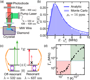
The experimental apparatus is illustrated in Fig. 4(a). A resonant (636-639 , 0.2 ) or off-resonant (532 , ) laser light is focused with a 0.5 numerical-aperture, 8 focal length aspheric lens onto the surface of a (111)-cut diamond housed in a continuous-flow cryostat (Janis ST-500). Fluorescence was collected using the same lens, spectrally filtered (within ), and detected with a Si photodiode. Microwaves were delivered by a m diameter copper wire running across the surface of the diamond. The temperature was measured with a diode located at the base of the cryostat’s sample holder.
The diamond used in this work, labeled S2 in [63], was grown under high-pressure-high-temperature conditions (HPHT) and initially contained ppm of substitutional nitrogen. It was then irradiated with electrons at a dose of in order to produce a uniform distribution of vacancies, and subsequently annealed at for two hours in order to facilitate the formation of NV centers by mobilizing the vacancies. After this treatment, the sample contains ppm of NV- and ppm of unconverted substitutional nitrogen or NV0 based on ZPL intensity measurements [63]. We note that this estimate of the NV density is larger than that of the charge-based model (see subsection II.2).
Appendix B Detuning Above ZPL
Shown in Fig. 5 is the dependence of the resonant ODMR lineshapes for a wide range optical detunings. For drives below ZPL, the positive-contrast peaks are clearly visible and are described quantitatively by our microscopic model (see section II). In contrast, for drives above ZPL, the positive-contrast peaks disappear with increasing detuning. We conjecture that this disappearance is related to the fact that the resonance condition is most likely to be met by the upper branch of the manifold at these detunings, but this branch is itself within the phonon-sideband of the lower branch. Hence, excited states of the upper branch will have shorter lifetimes than their lower branch counterparts, possibly rendering the linewidth of the associated optical transitions too large for the positive-contrast feature to emerge.
Appendix C Additional Details of the Resonant ODMR Model
In this appendix, we elaborate on four aspects of our microscopic model of resonant ODMR. First, we demonstrate that the electric field distribution arising from randomly placed charges can be accurately modeled by the analytic expression equation (1). Second, we discuss the single-NV primitive lineshape, , used in our analysis. Third, we provide the explicit expression for the off-resonant contribution to the resonant ODMR lineshape, . Finally, we extend our model to account for the background fluorescence of resonant ODMR, yielding the prediction of Fig. 3(b).
Electric field distribution: At its core, our microscopic model proposes that the NV is affected by internal electric fields arising from randomly placed point charges in the diamond lattice. To determine the electric field distribution, we numerically sampled random spatial configurations for charges at a given density and computed their net electric field at an arbitrary spatial point corresponding to the location of the NV. Empirically, we found that these Monte Carlo results were well approximated by Eq. (1), especially near the peak of the distribution, which is most relevant for our susceptibility analysis [Fig. 4(b)]. Incidentally, Eq. (1) corresponds to the electric field distribution owing to the nearest (single) charge at a renormalized density ; however, we consider this a mathematical coincidence. For our purposes, it is relevant only that Eq. (1) provides a convenient analytic expression to approximate the full electric field distribution generated by Monte Carlo simulations
Primitive lineshape: As discussed in the main text, the single-NV ODMR lineshape depends on an magnetic broadening parameter , arising from local magnetic fields, and a non-magnetic broadening parameter , due to microwave power broadening and strain. The difference between the two forms of broadening is that magnetic broadening adds in quadrature with the electric field splitting, while non-magnetic broadening is treated as an overall convolution. We model both forms of broadening as a Lorentzian distribution, where is the full-width-half-maximum (FWHM). Finally, we take into account the effective magnetic field, owing to the three distinct 14N nuclear states, i.e. . Altogether, the explicit form for is given by
| (14) |
where
is the lineshape with magnetic broadening alone.
Off-resonant contribution: The expression for the off-resonant contribution to the resonant ODMR spectra is structurally identical to the resonant case. The essential difference lies in replacing the kernel defining the resonant condition, , with a new kernel that quantifies the degree of off-resonant driving. Specifically, the off-resonant kernel, , can take three values: 0 if the optical drive is below both branches, 1 if it is between the two branches, and 2 if it is above both branches; this is because the phonon sidebands of each excited state branch can contribute to the off-resonant cross-section. Formalizing this physical picture, we obtain,
| (15) | ||||
| (16) |
Total fluorescence: The total fluorescence is determined by the fraction of resonant and off-resonant configurations. These fractions are given by
| (17) | ||||
| (18) |
where is the total number of configurations. The total fluorescence is a weighted sum of these two contributions:
| (19) |
where is the enhancement factor of the resonant mechanism. From single NV experiments, we estimate [91]. Up to overall rescaling, we can then calculate the predicted fluorescence as a function of detuning; this exhibits good agreement with the background fluorescence as shown in Fig. 3(b).
Appendix D Estimating Susceptibilities
As discussed in the main text, we extract the excited-state electric field susceptibilities by fitting our model to the measured splitting of the positive-contrast peak, , as a function optical detuning, . Here, we provide additional details on this procedure, including error estimation and the determination of model parameters, i.e. the charge density and broadening parameters.
To begin, we determine as a function of detuning from the experimentally measured ODMR spectra [Fig. 2(a)]. In particular, we identify the frequency of the local maximum, , associated with each positive-contrast peak and compute . The uncertainty on these estimates arises from shot noise in the resonant ODMR spectra, which causes the frequency of maximum florescence to vary between successive measurements. To determine this uncertainty, we perform a Monte Carlo simulation of Lorentzian lineshapes with Gaussian noise, whose strength is determined from the experimental data, and sample the frequency of local maximum; this yields the error bars shown in Fig. 2(b) and 7(a).
We next determine the three parameters required in our resonant ODMR model (see section II.2) other than the susceptibilities through the following independent calibration steps:
-
1.
Magnetic broadening, : We measure the resonant ODMR spectrum of an NV sub-ensemble with a significant magnetic field projection along its axis [Fig 6(a)]. Since this magnetic field suppresses electric field noise, the dominant source of remaining noise is due to inhomogeneous magnetic fields. Fitting this spectrum to three Lorentzians yields an magnetic linewidth [Fig. 6(a)].
-
2.
Charge density, : We measure a room-temperature, off-resonant ODMR spectrum without a bias magnetic field. The characteristic splitting observed in this spectrum is fit to our model of randomly placed charges, leading to a charge-density estimate of ppm.
-
3.
Non-magnetic broadening, : We perform a Lorentzian fit to the positive-contrast features of an ODMR spectrum measured with optical excitation near the zero-phonon-line (). This spectrum is chosen because it has minimal broadening due to electric fields. We subtract from the extracted linewidth and assume the remaining broadening arises from non-magnetic sources (e.g. microwave power broadening); this yields . We note that this parameter has only a minor effect on the susceptibility estimates.
Finally, we extract the susceptibility parameters by fitting our model to the empirical values for as a function of . In particular, we calculate the least-square error of the data compared to the predicted splittings from our resonant ODMR model, with and as the only free parameters [Fig. 7(a)]222In the vicinity of the positive-contrast peaks, the off-resonant configurations only contribute a flat background, and can hence be neglected in our fitting procedure. This eliminates and off-resonant linewidths as free parameters and thus simplifies the model we use to extract the susceptibilities. To check this approximation, we also extract the susceptibilities using the and off-resonant linewidths extracted from the spectrum (Table 1) and find that they are within statistical error of those determined from our simpler estimation procedure.. We find the -error is minimized at with a reduced- value of (with observations and fit parameters). By linearizing our model around the fitted values, we determine the confidence region of the susceptibility estimates [Fig. 7(b)] and estimate uncertainties of for , and for . We also estimate systematic errors by repeating the analysis with the values and indicated in Fig 6(b). This is shown in Fig. 7(b) and leads to a systematic error of for , and for . Summing in quadrature, we have a total error estimate of for and for .
A few additional remarks are in order. First, we note that our procedure, by focusing on the splitting of the ODMR spectra, depends primarily on the magnitude of the most-probable electric field (i.e. ) and not on the details of the full distribution. Second, in principle may depend on the temperature, optical excitation frequency, and excitation power, which would invalidate our assumption that can be determined from off-resonant room-temperature ODMR [41, 40, 93]. However, even if we relax this assumption, the optical transition linewidth provides an additional, independent constraint on the charge-density and susceptibilities. By demanding that simultaneously recover and the excited state linewidth, we find , where the super- (sub-) script indicates the upper (lower) bound. The systematic errors on the extracted susceptibilities concordantly increase to and for and respectively. Therefore, the essentials of our analysis and conclusions do not depend on an assumption of consistent (although our observations support this conclusion for ensemble measurements).
Appendix E Resonant ODMR Linewidth
The positive-contrast features shown in Fig. 2(a) exhibit not only a splitting which depends on the optical detuning, but also a linewidth which systematically increases with detuning (Fig. 8). Qualitatively, this effect can be understood as arising from the tail of the electric field distribution: If the electric field distribution decays very slowly, will be large since many nearly equal probability electric-field spheres will intersect the resonant cone at different values of .
While our microscopic model accounts for this general trend, it does not accurately predict the precise form of vs. (Fig. 8). Interestingly, this discrepancy suggests that our microscopic model is missing subtle aspects of the electric field distribution at large strengths / short distances. More formally, the trend that increases with (Fig. 8) indicates the relative decay rate of the electric-field distribution decreases at larger values of . This is characteristic of a polynomially decaying tail: if then , so the tail decays more slowly at larger resulting in larger . Indeed, one possible direction for future research is to quantitatively extract from at large . This could yield insight into the underlying short-range physics controlling the tail of the electric field distribution, such as whether charges are more likely to be localized in the vicinity of the NV center.
Appendix F Temperature Dependent Spectra
Our procedure for fitting the temperature-dependent ODMR spectra, shown in Fig. 1(a), relies on the same resonant ODMR model, susceptibility parameters, and charge density as in the previous sections. In addition, we find it necessary to vary (i) the ODMR contrast ratio and (ii) broadening parameters at each temperature. Here, we discuss the physical origin of the temperature dependence of these parameters.
Contrast: We attribute the change in contrast to the the fact that increasing temperature broadens the optical transition linewidth, which in turn reduces the density of resonant configurations at a given optical detuning, effectively reducing . Indeed, we find qualitatively that decreases with temperature, though we do not attempt to develop a quantitative model for it.
Broadening: Experimentally, we observe that off-resonant dips in the ODMR spectrum exhibit larger broadening than the positive-contrast peaks (see Fig. 1(a) in main text). We conjecture two possible causes of this additional broadening. First, there may be different degrees of light-narrowing in the resonant and off-resonant configurations. Light-narrowing arises because resonantly driven transitions experience a greater rate of optical pumping than transitions to the phonon-sideband, and hence have a different effective linewidth. In this setting, a greater rate of optical pumping actually reduces the effective linewidth [94]. Second, power broadening itself may not be well described by a convolution with a Lorentzian; indeed we find that this is the case even for off-resonant ODMR spectra under higher microwave power. Intuitively, large electric fields alter the matrix elements between ground-state sublevels, causing the degree of power-broadening to be electric field strength dependent. To account for this, we treat the off-resonant magnetic broadening parameter, , as a free parameter and find that its best-fit value is comparable to the non-magnetic broadening. We emphasize that this is a convenient way to account for the dependence of power broadening on electric field strength and does not constitute a meaningful estimate of the true broadening due to magnetic fields.
We note that both of these issues are artifacts of working in a microwave power-broadened regime, which is the case for the present temperature-dependent data. For extraction of susceptibilities, ODMR measurements were performed with lower microwave power, where these effects are suppressed.
| Temp. | |||||
| 2.0 | 4.0 | 20.0 | 27.0 | ||
| 2.0 | 4.0 | 16.0 | 16.0 | ||
| 2.0 | 4.0 | 12.0 | 15.0 | ||
| 2.0 | 4.0 | 9.0 | 8.0 |
Appendix G Sensitivity Estimates
Here, we provide additional details for estimating the sensitivity of our resonant electric-field sensing protocol. The estimates are calibrated based on the sample measured in this work, and then extrapolated to other densities using scaling arguments.
Let us begin by recalling that the sensitivity for an electric-field dependent count rate is given by
| (20) |
or equivalently,
| (22) |
In our sensing protocol, the fluorescence rate is determined by two effects: (i) the shift of the positive-contrast peaks, and (ii) the change in overall fluorescence. These effects contribute independently to the total signal, such that , where and capture the dependence of fluorescence on optical detuning and microwave frequency, respectively. The total sensitivity is then
| (23) |
which leads to the equation stated in the main text:
| (24) |
For simplicity, we define . The sensitivities can be decomposed as
| (25) | ||||
| (26) |
where is the linewidth (lineshape factor) associated with the ground and excited states, is the count rate, is the maximum CW contrast of the resonant ODMR peaks, is the ratio of photons resulting from resonant fluorescence to total fluorescence, and are the effective ground- and excited-state susceptibilities, respectively.
For our estimates, we assume the ground state ODMR lineshape is Lorentzian, such that , and we use the excited-state susceptibility determined in our work: ; moreover, we determine and from our model [Fig. 9(a)] and from experimental data [Fig. 3(b)], respectively. The remaining parameters are discussed below.
G.1 Parameter calibration
Linewidths: We model the ODMR and optical transition linewidths as containing both an intrinsic broadening and an electric-field induced broadening:
| (27) |
where is a normalized NV density, . The ground state intrinsic broadening, , is typically dominated by paramagnetic impurities and is modeled by [70]
| (28) |
where represent the concentrations of and uncharged substitutional nitrogen defects, respectively. From [70] we obtain and . For impurity concentrations, we assume a natural abundance of ( or ppm) and that — i.e., a conversion ratio, which is among the best typically observed [71]. Since the intrinsic excited-state broadening is less well-understood, and certainly not limited by paramagnetic impurities, we adopt the simple density-independent model [95, 78]. Finally, we calibrate the charge-induced linewidths against our sample ( ppm), yielding and . We note that here, and throughout our sensitivity estimates, we will assume that the charge environment consists primarily of other uniformly distributed NVs and charge donors, such that (see subsection II.2).
Fluorescence rate: The overall fluorescence rate contains contributions from the resonant and off-resonant configurations. The former is proportional to the density of resonant configurations, and therefore is inversely proportional to the optical transition linewidth. Thus, the fluorescence from resonant configurations can be modeled as
| (29) |
where is the fluorescence rate for a single, off-resonantly driven NV orientation, is the fluorescence enhancement factor for resonant configurations, and is a density-independent prefactor. To determine , we compare the resonant fluorescence at the optimal detuning to the off-resonant fluorescence for detunings far above the ZPL [Fig. 9(b)]. This yields , corresponding to ; for an optimal sample, we estimate that can reach at ppb.
To determine the overall count rate, we take into account the fact that our sensing protocol includes signals from one resonant NV orientation and three off-resonant orientations. This is because the bias electric field required to lift the excited-state degeneracy pushes the excited state of three orientations below the excited state of the target orientation, so they are excited by the off-resonant mechanism. In particular, assuming a (111)-cut diamond, the fluorescence rate due to off-resonant orientations is 333The factor of 5/3 arises because the three off-resonant groups are not perpendicular to the laser polarization [102].. In combination, the total count rate is
| (30) |
We note that depends on the specific optical setup (e.g. illumination volume, laser power, and collection efficiency). We determine this constant for a similar setup as described in [29] 444In particular, we rescale their reported count rate by the ratio of our sample’s NV density to their sample’s density and correct for a difference in laser polarization. We also divide by , since only one NV crystallographic orientation will be used in the sensing protocol.. The final count rate for our sample and for an optimal sample are reported in Table 2.
Finally, for the room-temperature sensitivity estimate (Fig. 3), we additionally adjust to account for the decrease in the Debye-Waller factor with temperature. We estimate the Debye-Waller factor decreases by at compared to , degrading the sensitivity by [98, 99].
| DC Electrometry | T | |||||||||
| Method | (ppm) | () | () | () | () | (counts/) | () | |||
| Single NV - G.S. [16] | - | - | 0.05 | 0.77 | 17 | 100 | 0.3 | 760 | ||
| Single NV - E.S. [100] | - | - | 13 | 0.77 | 2500 | 1 | 0.29 | |||
| EIT Ensemble [78] | - | 1.0 | 0.77 | 9.8 | 0.022 | 0.20 | ||||
| Off-res. Ensemble [29] (optimized) | - | 1.0 | 0.77 | 17 | 0.02 | 0.10 | ||||
| Res. Ensemble | 0.39 | 0.54 | 0.021 | |||||||
| (Our sample) | 200 | 3.9 | 0.77 | 6.97 | 0.11 | 0.077 | ||||
| Total | - | - | - | - | - | 0.017 | ||||
| Res. Ensemble | 0.39 | 0.98 | 0.0014 | |||||||
| (Low-density sample) | 2.3 | 0.25 | 0.77 | 6.97 | 0.21 | 0.016 | ||||
| Total | - | - | - | - | - | 0.0013 | ||||
| Res. Ensemble | 0.39 | 0.98 | 0.0015 | |||||||
| ([] = 99.995% purified) | 0.8 | 0.017 | 0.77 | 6.97 | 0.21 | 0.0016 | ||||
| Total | - | - | - | - | - | |||||
Contrast: We first estimate the maximum CW contrast of the positive-contrast peaks, , from the experimental data [Fig. 9(c)] 555For a (111)-cut diamond, , where is the experimentally observed contrast. This factor is also related to the laser polarization [102]. However, of the total counts, only the resonant fraction, , contributes to sensing. Therefore, the actual contrast of the resonant ODMR peaks is ; meanwhile, for sensing via direct variation in fluorescence (), the relevant contrast is . For a (111)-cut sample, we have
| (31) |
where is the resonant enhancement factor defined in (29).
Bias electric field: In addition to the sensitivity estimates provided in the manuscript, we estimate the bias field required to spectrally isolate the crystallographic orientation used in our sensing protocol [Fig. 9(d)]. Given a bias field parallel to one of the NV groups, three other groups will actually be shifted by the electric field below the target group since . Therefore, we determine this bias field by demanding the lowest-energy NV group parallel to the bias field is at least above the lowest three NV groups.
G.2 Scaling with density
Here, we determine how sensitivity degrades in the high-density regime. We consider an ideal limit for which there is minimal charge broadening, i.e. and no density-dependent broadening other than internal electric-fields. As discussed above, in the charge-dominated regime the ODMR and optical transition linewidths () are proportional to the average electric field strength, which scales as . In this regime, we also have and , implying and . Thus the sensitivity scaling at high-densities is given by
| (32) |
as stated in the main text (Fig. 3). The scaling for typical electrometry protocols may be similarly determined. In this case, all photons are scattered off-resonantly and is no longer relevant in the sensitivity expressions. Then
| (33) |
as shown in Fig. 3 of the main text.
G.3 Isotopically Purified Samples
We note that for isotopically purified samples the relative contributions of and may be comparable (see Tab. 2). To illustrate this, let us consider the sensitivity of NV electrometry protocols assuming a concentration of ppm ([] = 99.995% purified) as utilized in recently optimized samples [70, 71]; indeed, such isotopically purified samples have been of tremendous recent interest for applications to precision metrology [70]. Assuming an excited state broadening of GHz, we find that and at the optimal NV density ppb.
G.4 Fine Structure
Our sensitivity model assumes that electric-field induced splitting dominates the fine structure. Under this assumption, it is sufficient to consider two three-fold degenerate orbital degrees of freedom in determining the resonance conditions. However, this assumption breaks down when the splitting due to internal electric fields of the diamond becomes comparable to the intrinsic hyperfine effects of the manifold, whose typical magnitude is [61]. Based on our extracted susceptibilities, we estimate this occurs for NV densities . For densities below this threshold, it is still possible to perform resonant sensing using individual sublevels; in particular, one should probe a pair of sublevels ( or ) which are linearly sensitive to electric fields [61]. In this regime, the sensitivity would be determined entirely by the change in overall fluorescence, i.e. .
Appendix H Theoretical Estimates of Susceptibilities
In this section, we discuss the physical origin of the NV’s electric field susceptibility in both the ground and excited state, and compare the measured susceptibility parameters to theoretical estimates (Table 3).
H.1 Excited state
While it is well understood that the orbital doublet nature of the excited state allows for a linear Stark shift, the microscopic origin of this shift can in principle be explained by two different mechanisms [61]. One mechanism, the electronic effect, is based on the polarization of the NV’s electronic wavefunction. The second mechanism, the ionic effect, consists of the relative displacement of the ions and is thus closely related to piezoelectricity. The two effects are indistinguishable from a group theoretic perspective and, in general, both will contribute to the total susceptibility. Below we estimate the susceptibilities based on the electronic effect and find good agreement with the measured values (Table 3). On the other hand, the ionic effect was previously estimated with ab initio simulations and was found to be on the same order of magnitude [61]. Thus, a more precise calculation of the excited susceptibilities should take into account both effects.
| (Hz cm/V) | (Hz cm/V) | |
| E.S. measured (this work) | ||
| E.S. electronic effect | ||
| G.S. measured [28] | ||
| G.S. spin-spin effect |
To estimate the electronic effect, we consider the molecular model of the defect center, in which the NV’s single-particle orbitals are constructed from non-overlapping atomic orbitals, , centered on the three carbon ions and the nitrogen ion, respectively [62, 61]. In particular, the single-particle orbitals are given by
| (34) | ||||
| (35) | ||||
| (36) |
where is the carbon orbital that lies in the plane, and is determined from density functional theory (DFT) calculations [103]666We note that there is a fourth state with the same symmetry properties as (i.e. transforms according to the totally symmetric irreducible representation), but it is higher in energy than the other three and therefore not relevant for this discussion [61]. These orbitals are combined to form the ground state
| (37) |
and the two excited states
| (38) | ||||
| (39) |
From first-order perturbation theory, the electric field susceptibility is determined by the permanent dipole of the excited state. For the transverse susceptibility, it is sufficient to calculate the dipole moment along the -axis, which is diagonal in the basis:
| (40) |
where are the single particle positions and is the elementary charge. In the single-particle basis, this reduces to
| (41) | ||||
| (42) |
where we have approximated the full integral by assuming non-overlapping atomic orbitals. For the longitudinal direction, the relevant term is the relative dipole moment between between the ground and excited state. This is given by
| (43) | ||||
| (44) | ||||
| (45) |
Inserting orbital expectation values from DFT calculations, we obtain and [103, 105]. This yields susceptibility estimates of MHz/(V/cm), in good agreement with the values measured in this work (Table 3).
H.2 Ground state
The ground state of the NV center is an orbital singlet, leading to the naive expectation that a linear Stark effect is disallowed. This, however, contradicts experimental observation of [28]. The conventional explanation is that the ground state inherits a permanent dipole moment from the excited state due to spin-orbit coupling [106, 107]. While such coupling is indeed present, its magnitude is likely insufficient to account for the measured transverse field susceptibility. More recently, it was suggested that the ground state transverse susceptibility arises from the interplay between electric fields and the dipolar spin-spin interaction [107]. In particular, the effect is as follows: At first order in perturbation theory, the ground state wavefunction is mixed with the excited state by the presence of an electric field; this perturbation then couples to the ground-state spin degrees of freedom via the dipolar spin-spin interaction. Below we estimate the magnitude of the effect (which was not reported in [107]) and find good agreement with the known ground state transverse susceptibility (Table 3). We also hasten to emphasize that this effect only occurs to leading order for transverse electric fields, which naturally explains the 50-fold anisotropy between and .
As in the case of the excited state, it is sufficient to consider the transverse susceptibility for a field along the -axis. At first order in perturbation theory, an electric field mixes the ground state with the excited state :
| (46) |
where is the elementary charge, and is the energy splitting between the ground and excited state. is the dipole moment associated with the transition between the states,
| (47) |
In the single-particle basis, this becomes
| (48) | ||||
| (49) |
To determine the effect on the ground-state spin degrees of freedom, it is then necessary to consider the dipolar spin-spin interaction, given by
| (50) |
where , is the Bohr magneton, is the NV gyromagnetic ratio, are spin-1 operators, and is the relative displacement between the two particles. In the absence of an external perturbation, the orbital degrees of freedom are integrated with respect to the ground-state wavefunction , and the only non-vanishing term is the ground-state splitting, . For the perturbed wavefunction , there is an additional non-vanishing term, corresponding to a ground-state Stark shift:
| (51) |
The magnitude of is given by
| (52) |
with
| (53) | ||||
| (54) |
Assuming non-overlapping orbitals, this simplifies to
| (55) |
We further approximate the two-particle integrals with the semiclassical position of each particle individually [107, 105]:
| (56) | ||||
| (57) |
where and in the final expressions we utilized the triangular symmetry of the carbon orbitals. This leads to
| (58) |
Altogether, this predicts a susceptibility of , which is within a factor of 5 of the measured value.
Crucially, the spin-spin effect also provides a group theoretic explanation for the large anisotropy between the ground state transverse and longitudinal susceptibilities. In particular, the longitudinal dipole moment between the ground and excited states,
| (59) |
vanishes due to symmetry, implying that only a transverse electric field can mix the ground and excited states to leading order. We thus postulate that the relatively strong transverse susceptibility arises from the proposed spin-spin effect, while the weak longitudinal effect arises from entirely different physical origin, e.g. based on spin-orbit coupling or the ionic (piezoelectric) effect.
References
- [1] LT Hall, GCG Beart, EA Thomas, DA Simpson, LP McGuinness, JH Cole, JH Manton, RE Scholten, Fedor Jelezko, Jörg Wrachtrup, et al. High spatial and temporal resolution wide-field imaging of neuron activity using quantum nv-diamond. Scientific reports, 2:401, 2012.
- [2] Lei Jin, Zhou Han, Jelena Platisa, Julian RA Wooltorton, Lawrence B Cohen, and Vincent A Pieribone. Single action potentials and subthreshold electrical events imaged in neurons with a fluorescent protein voltage probe. Neuron, 75(5):779–785, 2012.
- [3] Fei Huang, Venkata Ananth Tamma, Zahra Mardy, Jonathan Burdett, and H Kumar Wickramasinghe. Imaging nanoscale electromagnetic near-field distributions using optical forces. Scientific reports, 5:10610, 2015.
- [4] Rudra Sankar Dhar, Seyed Ghasem Razavipour, Emmanuel Dupont, Chao Xu, Sylvain Laframboise, Zbig Wasilewski, Qing Hu, and Dayan Ban. Direct nanoscale imaging of evolving electric field domains in quantum structures. Scientific reports, 4:7183, 2014.
- [5] Gilad Ben-Shach, Arbel Haim, Ian Appelbaum, Yuval Oreg, Amir Yacoby, and Bertrand I. Halperin. Detecting Majorana modes in one-dimensional wires by charge sensing. Physical Review B, 91(4):045403, January 2015.
- [6] R. J. Schoelkopf, P. Wahlgren, A. A. Kozhevnikov, P. Delsing, and D. E. Prober. The Radio-Frequency Single-Electron Transistor (RF-SET): A Fast and Ultrasensitive Electrometer. Science, 280(5367):1238–1242, May 1998.
- [7] L. Tosi, D. Vion, and H. le Sueur. Design of a Cooper-Pair Box Electrometer for Application to Solid-State and Astroparticle Physics. Physical Review Applied, 11(5):054072, May 2019.
- [8] A. C. Johnson, J. R. Petta, C. M. Marcus, M. P. Hanson, and A. C. Gossard. Singlet-triplet spin blockade and charge sensing in a few-electron double quantum dot. Physical Review B, 72(16):165308, October 2005.
- [9] A. N. Vamivakas, Y. Zhao, S. Fält, A. Badolato, J. M. Taylor, and M. Atat ure. Nanoscale Optical Electrometer. Physical Review Letters, 107(16):166802, October 2011.
- [10] Andrew N Cleland and Michael L Roukes. A nanometre-scale mechanical electrometer. Nature, 392(6672):160–162, 1998.
- [11] J Scott Bunch, Arend M Van Der Zande, Scott S Verbridge, Ian W Frank, David M Tanenbaum, Jeevak M Parpia, Harold G Craighead, and Paul L McEuen. Electromechanical resonators from graphene sheets. Science, 315(5811):490–493, 2007.
- [12] Haoquan Fan, Santosh Kumar, Jonathon Sedlacek, Harald Kübler, Shaya Karimkashi, and James P. Shaffer. Atom based RF electric field sensing. Journal of Physics B: Atomic, Molecular and Optical Physics, 48(20):202001, September 2015.
- [13] Adrien Facon, Eva-Katharina Dietsche, Dorian Grosso, Serge Haroche, Jean-Michel Raimond, Michel Brune, and Sébastien Gleyzes. A sensitive electrometer based on a Rydberg atom in a Schrödinger-cat state. Nature, 535(7611):262–265, July 2016.
- [14] Santosh Kumar, Haoquan Fan, Harald Kübler, Jiteng Sheng, and James P. Shaffer. Atom-Based Sensing of Weak Radio Frequency Electric Fields Using Homodyne Readout. Scientific Reports, 7(1):1–10, February 2017.
- [15] David D. Awschalom, Ronald Hanson, Jörg Wrachtrup, and Brian B. Zhou. Quantum technologies with optically interfaced solid-state spins. Nature Photonics, 12(9):516–527, September 2018.
- [16] Florian Dolde, Helmut Fedder, Marcus W Doherty, Tobias Nöbauer, Florian Rempp, Gopalakrishnan Balasubramanian, Thomas Wolf, Friedemann Reinhard, Lloyd CL Hollenberg, Fedor Jelezko, et al. Electric-field sensing using single diamond spins. Nature Physics, 7(6):459, 2011.
- [17] J. M. Taylor, P. Cappellaro, L. Childress, L. Jiang, D. Budker, P. R. Hemmer, A. Yacoby, R. Walsworth, and M. D. Lukin. High-sensitivity diamond magnetometer with nanoscale resolution. Nature Physics, 4(10):810–816, October 2008.
- [18] Gary Wolfowicz, Christopher P Anderson, Samuel J Whiteley, and David D Awschalom. Heterodyne detection of radio-frequency electric fields using point defects in silicon carbide. Applied Physics Letters, 115(4):043105, 2019.
- [19] Robert Amsüss, Ch Koller, Tobias Nöbauer, Stefan Putz, Stefan Rotter, Kathrin Sandner, Stephan Schneider, Matthias Schramböck, Georg Steinhauser, Helmut Ritsch, et al. Cavity qed with magnetically coupled collective spin states. Physical review letters, 107(6):060502, 2011.
- [20] DM Toyli, DJ Christle, A Alkauskas, BB Buckley, CG Van de Walle, and DD Awschalom. Measurement and control of single nitrogen-vacancy center spins above 600 k. Physical Review X, 2(3):031001, 2012.
- [21] Marcus W Doherty, Viktor V Struzhkin, David A Simpson, Liam P McGuinness, Yufei Meng, Alastair Stacey, Timothy J Karle, Russell J Hemley, Neil B Manson, Lloyd CL Hollenberg, et al. Electronic properties and metrology applications of the diamond nv- center under pressure. Physical review letters, 112(4):047601, 2014.
- [22] Margarita Lesik, Thomas Plisson, Loïc Toraille, Justine Renaud, Florent Occelli, Martin Schmidt, Olivier Salord, Anne Delobbe, Thierry Debuisschert, Loïc Rondin, Paul Loubeyre, and Jean-François Roch. Magnetic measurements on micrometer-sized samples under high pressure using designed NV centers. Science, 366(6471):1359–1362, December 2019.
- [23] King Yau Yip, Kin On Ho, King Yiu Yu, Yang Chen, Wei Zhang, S. Kasahara, Y. Mizukami, T. Shibauchi, Y. Matsuda, Swee K. Goh, and Sen Yang. Measuring magnetic field texture in correlated electron systems under extreme conditions. Science, 366(6471):1355–1359, December 2019.
- [24] S. Hsieh, P. Bhattacharyya, C. Zu, T. Mittiga, T. J. Smart, F. Machado, B. Kobrin, T. O. Höhn, N. Z. Rui, M. Kamrani, S. Chatterjee, S. Choi, M. Zaletel, V. V. Struzhkin, J. E. Moore, V. I. Levitas, R. Jeanloz, and N. Y. Yao. Imaging stress and magnetism at high pressures using a nanoscale quantum sensor. Science, 366(6471):1349–1354, December 2019.
- [25] Georg Kucsko, Peter C Maurer, Norman Ying Yao, MICHAEL Kubo, Hyun Jong Noh, Po Kam Lo, Hongkun Park, and Mikhail D Lukin. Nanometre-scale thermometry in a living cell. Nature, 500(7460):54, 2013.
- [26] Romana Schirhagl, Kevin Chang, Michael Loretz, and Christian L Degen. Nitrogen-vacancy centers in diamond: nanoscale sensors for physics and biology. Annual review of physical chemistry, 65:83–105, 2014.
- [27] H. Kraus, V. A. Soltamov, F. Fuchs, D. Simin, A. Sperlich, P. G. Baranov, G. V. Astakhov, and V. Dyakonov. Magnetic field and temperature sensing with atomic-scale spin defects in silicon carbide. Scientific Reports, 4(1):5303, July 2014.
- [28] Eric Van Oort and Max Glasbeek. Electric-field-induced modulation of spin echoes of nv centers in diamond. Chemical Physics Letters, 168(6):529–532, 1990.
- [29] Edward H. Chen, Hannah A. Clevenson, Kerry A. Johnson, Linh M. Pham, Dirk R. Englund, Philip R. Hemmer, and Danielle A. Braje. High-sensitivity spin-based electrometry with an ensemble of nitrogen-vacancy centers in diamond. Physical Review A, 95(5):053417, May 2017.
- [30] Julia Michl, Jakob Steiner, Andrej Denisenko, André Bülau, André Zimmermann, Kazuo Nakamura, Hitoshi Sumiya, Shinobu Onoda, Philipp Neumann, Junichi Isoya, and Jörg Wrachtrup. Robust and Accurate Electric Field Sensing with Solid State Spin Ensembles. Nano Letters, 19(8):4904–4910, August 2019.
- [31] PV Klimov, AL Falk, BB Buckley, and DD Awschalom. Electrically driven spin resonance in silicon carbide color centers. Physical Review Letters, 112(8):087601, 2014.
- [32] Abram L Falk, Paul V Klimov, Bob B Buckley, Viktor Ivády, Igor A Abrikosov, Greg Calusine, William F Koehl, Ádám Gali, and David D Awschalom. Electrically and mechanically tunable electron spins in silicon carbide color centers. Physical review letters, 112(18):187601, 2014.
- [33] Takayuki Iwasaki, Wataru Naruki, Kosuke Tahara, Toshiharu Makino, Hiromitsu Kato, Masahiko Ogura, Daisuke Takeuchi, Satoshi Yamasaki, and Mutsuko Hatano. Direct nanoscale sensing of the internal electric field in operating semiconductor devices using single electron spins. ACS nano, 11(2):1238–1245, 2017.
- [34] Amila Ariyaratne, Dolev Bluvstein, Bryan A Myers, and Ania C Bleszynski Jayich. Nanoscale electrical conductivity imaging using a nitrogen-vacancy center in diamond. Nature communications, 9(1):2406, 2018.
- [35] Ilya Khivrich and Shahal Ilani. Electric and magnetic field nano-sensing using a new, atomic-like qubit in a carbon nanotube. arXiv preprint arXiv:1908.08249, 2019.
- [36] Christopher P. Anderson, Alexandre Bourassa, Kevin C. Miao, Gary Wolfowicz, Peter J. Mintun, Alexander L. Crook, Hiroshi Abe, Jawad Ul Hassan, Nguyen T. Son, Takeshi Ohshima, and David D. Awschalom. Electrical and optical control of single spins integrated in scalable semiconductor devices. Science, 366(6470):1225–1230, 2019.
- [37] Qi Zhang, Guangchong Hu, Gabriele G. de Boo, Miloš Rančić, Brett C. Johnson, Jeffrey C. McCallum, Jiangfeng Du, Matthew J. Sellars, Chunming Yin, and Sven Rogge. Single Rare-Earth Ions as Atomic-Scale Probes in Ultrascaled Transistors. Nano Letters, 19(8):5025–5030, August 2019.
- [38] Vittorio Giovannetti, Seth Lloyd, and Lorenzo Maccone. Quantum-enhanced measurements: beating the standard quantum limit. Science, 306(5700):1330–1336, 2004.
- [39] Ph. Tamarat, T. Gaebel, J. R. Rabeau, M. Khan, A. D. Greentree, H. Wilson, L. C. L. Hollenberg, S. Prawer, P. Hemmer, F. Jelezko, and J. Wrachtrup. Stark Shift Control of Single Optical Centers in Diamond. Physical Review Letters, 97(8):083002, August 2006.
- [40] V. M. Acosta, C. Santori, A. Faraon, Z. Huang, K.-M. C. Fu, A. Stacey, D. A. Simpson, K. Ganesan, S. Tomljenovic-Hanic, A. D. Greentree, S. Prawer, and R. G. Beausoleil. Dynamic Stabilization of the Optical Resonances of Single Nitrogen-Vacancy Centers in Diamond. Physical Review Letters, 108(20):206401, May 2012.
- [41] L. C. Bassett, F. J. Heremans, C. G. Yale, B. B. Buckley, and D. D. Awschalom. Electrical tuning of single nitrogen-vacancy center optical transitions enhanced by photoinduced fields. Phys. Rev. Lett., 107:266403, Dec 2011.
- [42] Maximilian Rühl, Lena Bergmann, Michael Krieger, and Heiko B. Weber. Stark Tuning of the Silicon Vacancy in Silicon Carbide. Nano Letters, 20(1):658–663, January 2020.
- [43] Alexander D. White, Daniil M. Lukin, Melissa A. Guidry, Rahul Trivedi, Naoya Morioka, Charles Babin, Florian Kaiser, Jawad Ul-Hassan, Nguyen Tien Son, Takeshi Ohshima, Praful Vasireddy, Mamdouh Nasr, Emilio Nanni, Jörg Wrachtrup, and Jelena Vučković. Static and Dynamic Stark Tuning of the Silicon Vacancy in Silicon Carbide. In Conference on Lasers and Electro-Optics, page FTu3D.1, Washington, DC, 2020. OSA.
- [44] Gichang Noh, Daebok Choi, Jin-Hun Kim, Dong-Gil Im, Yoon-Ho Kim, Hosung Seo, and Jieun Lee. Stark Tuning of Single-Photon Emitters in Hexagonal Boron Nitride. Nano Letters, 18(8):4710–4715, August 2018.
- [45] T Müller, I Aharonovich, L Lombez, Y Alaverdyan, A N Vamivakas, S Castelletto, F Jelezko, J Wrachtrup, S Prawer, and M Atatüre. Wide-range electrical tunability of single-photon emission from chromium-based colour centres in diamond. New Journal of Physics, 13(7):075001, July 2011.
- [46] Roland Nagy, Matthias Niethammer, Matthias Widmann, Yu-Chen Chen, Péter Udvarhelyi, Cristian Bonato, Jawad Ul Hassan, Robin Karhu, Ivan G Ivanov, Nguyen Tien Son, et al. High-fidelity spin and optical control of single silicon-vacancy centres in silicon carbide. Nature communications, 10(1):1–8, 2019.
- [47] Charles F. de las Casas, David J. Christle, Jawad Ul Hassan, Takeshi Ohshima, Nguyen T. Son, and David D. Awschalom. Stark tuning and electrical charge state control of single divacancies in silicon carbide. Applied Physics Letters, 111(26):262403, December 2017.
- [48] P. Kehayias, M. Mrózek, V. M. Acosta, A. Jarmola, D. S. Rudnicki, R. Folman, W. Gawlik, and D. Budker. Microwave saturation spectroscopy of nitrogen-vacancy ensembles in diamond. Physical Review B, 89(24):245202, June 2014.
- [49] Arthur L. Schawlow. Spectroscopy in a new light. Reviews of Modern Physics, 54(3):697–707, July 1982.
- [50] Marcus W Doherty, Neil B Manson, Paul Delaney, Fedor Jelezko, Jörg Wrachtrup, and Lloyd CL Hollenberg. The nitrogen-vacancy colour centre in diamond. Physics Reports, 528(1):1–45, 2013.
- [51] Rinat Akhmedzhanov, Lev Gushchin, Nikolay Nizov, Vladimir Nizov, Dmitry Sobgayda, Ilya Zelensky, and Philip Hemmer. Optically detected magnetic resonance in negatively charged nitrogen-vacancy centers in diamond under resonant optical excitation at cryogenic temperatures. Physical Review A, 94(6):063859, December 2016.
- [52] Rinat Akhmedzhanov, Lev Gushchin, Nikolay Nizov, Vladimir Nizov, Dmitry Sobgayda, Ilya Zelensky, and Philip Hemmer. Microwave-free magnetometry based on cross-relaxation resonances in diamond nitrogen-vacancy centers. Physical Review A, 96(1):013806, July 2017.
- [53] Thomas Mittiga, Satcher Hsieh, Chong Zu, Bryce Kobrin, Francisco Machado, Prabudhya Bhattacharyya, NZ Rui, Andrey Jarmola, Soonwon Choi, Dmitry Budker, et al. Imaging the local charge environment of nitrogen-vacancy centers in diamond. Physical review letters, 121(24):246402, 2018.
- [54] Dolev Bluvstein, Zhiran Zhang, and Ania C Bleszynski Jayich. Identifying and mitigating charge instabilities in shallow diamond nitrogen-vacancy centers. Physical review letters, 122(7):076101, 2019.
- [55] J. Kölbl, M. Kasperczyk, B. Bürgler, A. Barfuss, and P. Maletinsky. Determination of intrinsic effective fields and microwave polarizations by high-resolution spectroscopy of single nitrogen-vacancy center spins. New Journal of Physics, 21(11):113039, November 2019.
- [56] We would also like to point out that our protocol’s DC sensitivity compares favorably to the best reported NV-ensemble based AC sensing method [30]. In particular, assuming equal illumination volumes, our DC sensitivity is one order of magnitude better than the AC sensitivity reported in [30] (e.g. the adjusted AC sensitivity of [30] for an illumination volume of would be ).
- [57] Kai-Mei C. Fu, Charles Santori, Paul E. Barclay, Lachlan J. Rogers, Neil B. Manson, and Raymond G. Beausoleil. Observation of the Dynamic Jahn-Teller Effect in the Excited States of Nitrogen-Vacancy Centers in Diamond. Physical Review Letters, 103(25):256404, December 2009.
- [58] Lattice strain effects have also been shown to lead to a split resonance in single NV centers [55]. However, typical strain fields result in both a shifting and splitting of the resonance. In ensembles, this naturally leads to a single broad peak instead of the observed split resonance [53]. In the case of electric fields, due to the large anisotropy between the transverse and longitudinal susceptibilities, local charges generically split the sub-levels without significant shifting.
- [59] We define a resonant configuration, at a given detuning, as a combination of transverse and longitudinal electric fields which cause the NV’s ground to excited state transition to be resonantly driven by the optical excitation. Note that the resonance condition does not depend on the direction of the transverse component of the field in the plane perpendicular to the NV axis.
- [60] S. Bhagavantam and D. a. a. S. Narayana Rao. Dielectric Constant of Diamond. Nature, 161(4097):729–729, May 1948.
- [61] J R Maze, A Gali, E Togan, Y Chu, A Trifonov, E Kaxiras, and M D Lukin. Properties of nitrogen-vacancy centers in diamond: the group theoretic approach. New Journal of Physics, 13(2):025025, February 2011.
- [62] M. W. Doherty, N. B. Manson, P. Delaney, and L. C. L. Hollenberg. The negatively charged nitrogen-vacancy centre in diamond: the electronic solution. New Journal of Physics, 13(2):025019, February 2011.
- [63] V. M. Acosta, E. Bauch, M. P. Ledbetter, C. Santori, K.-M. C. Fu, P. E. Barclay, R. G. Beausoleil, H. Linget, J. F. Roch, F. Treussart, S. Chemerisov, W. Gawlik, and D. Budker. Diamonds with a high density of nitrogen-vacancy centers for magnetometry applications. Phys. Rev. B, 80:115202, Sep 2009.
- [64] At small optical detunings, the highest-probability electric-field sphere (i.e. that of radius ) will actually intersect the resonant cone twice, leading the to the expectation of two resonant peaks. However, the width of around broadens these features, resulting a single, slightly asymmetric peak.
- [65] We note, however, that photo-ionization effects could cause the charge density to depend on excitation wavelength, although we do not observe this in our measurements [108, 40, 93].
- [66] Sarvagya Sharma, Chris Hovde, Douglas H. Beck, and Fahad Alghannam. Imaging Strain and Electric Fields in NV Ensembles using Stark Shift Measurements. arXiv preprint arXiv:1802.08767v1, February 2018.
- [67] Chris Hovde, Sarvagya Sharma, Fahad Alghannam, and Douglas H. Beck. Measuring electric fields with nitrogen-vacancy ensembles for neutron electric dipole moment experiments. In Laurence P. Sadwick and Tianxin Yang, editors, Terahertz, RF, Millimeter, and Submillimeter-Wave Technology and Applications XI, volume 10531, pages 103 – 110. International Society for Optics and Photonics, SPIE, 2018.
- [68] Sarvagya Sharma, Chris Hovde, Fahad Alghannam, and Douglas H. Beck. Electric and magnetic sensing with NV ensembles in diamonds. In Manijeh Razeghi, editor, Quantum Sensing and Nano Electronics and Photonics XIV, volume 10111, pages 436 – 444. International Society for Optics and Photonics, SPIE, 2017.
- [69] Rui Li, Fei Kong, Pengju Zhao, Zhi Cheng, Zhuoyang Qin, Mengqi Wang, Qi Zhang, Pengfei Wang, Ya Wang, Fazhan Shi, and Jiangfeng Du. Nanoscale Electrometry Based on a Magnetic-Field-Resistant Spin Sensor. Physical Review Letters, 124(24):247701, June 2020.
- [70] Andrew M. Edmonds, Connor A. Hart, Matthew J. Turner, Pierre-Olivier Colard, Jennifer M. Schloss, Kevin Olsson, Raisa Trubko, Matthew L. Markham, Adam Rathmill, Ben Horne-Smith, Wilbur Lew, Arul Manickam, Scott Bruce, Peter G. Kaup, Jon C. Russo, Michael J. DiMario, Joseph T. South, Jay T. Hansen, Daniel J. Twitchen, and Ronald L. Walsworth. Generation of nitrogen-vacancy ensembles in diamond for quantum sensors: Optimization and scalability of CVD processes. arXiv:2004.01746 [cond-mat, physics:quant-ph], April 2020.
- [71] John F. Barry, Jennifer M. Schloss, Erik Bauch, Matthew J. Turner, Connor A. Hart, Linh M. Pham, and Ronald L. Walsworth. Sensitivity optimization for NV-diamond magnetometry. Reviews of Modern Physics, 92(1):015004, March 2020.
- [72] Interestingly, the first of these effects has also been explored in the context of a complementary MW-free magnetometry protocol [52].
- [73] In Appendix G, we show that the necessary fields are similar in scale to those required in [29].
- [74] Other perturbations to the NV level structure, such as strain and magnetic fields, can exacerbate ensemble broadening. For this discussion, we restrict attention to the ideal limit where there is minimal charge () and there are no other significant density dependent sources of inhomogenous broadening.
- [75] Linh Pham. Magnetic Field Sensing with Nitrogen-Vacancy Color Centers in Diamond. PhD thesis, Harvard University, 2013.
- [76] Gopalakrishnan Balasubramanian, Philipp Neumann, Daniel Twitchen, Matthew Markham, Roman Kolesov, Norikazu Mizuochi, Junichi Isoya, Jocelyn Achard, Johannes Beck, Julia Tissler, Vincent Jacques, Philip R. Hemmer, Fedor Jelezko, and Jörg Wrachtrup. Ultralong spin coherence time in isotopically engineered diamond. Nature Materials, 8(5):383–387, May 2009.
- [77] A. Batalov, V. Jacques, F. Kaiser, P. Siyushev, P. Neumann, L. J. Rogers, R. L. McMurtrie, N. B. Manson, F. Jelezko, and J. Wrachtrup. Low Temperature Studies of the Excited-State Structure of Negatively Charged Nitrogen-Vacancy Color Centers in Diamond. Physical Review Letters, 102(19):195506, May 2009.
- [78] V. M. Acosta, K. Jensen, C. Santori, D. Budker, and R. G. Beausoleil. Electromagnetically induced transparency in a diamond spin ensemble enables all-optical electromagnetic field sensing. Phys. Rev. Lett., 110:213605, May 2013.
- [79] We emphasize that here we are referring to ensemble broadening; single NVs can exhibit nearly lifetime-limited excited state linewidths [109, 39, 110, 111].
- [80] Chang S. Shin, Claudia E. Avalos, Mark C. Butler, David R. Trease, Scott J. Seltzer, J. Peter Mustonen, Daniel J. Kennedy, Victor M. Acosta, Dmitry Budker, Alexander Pines, and Vikram S. Bajaj. Room-temperature operation of a radiofrequency diamond magnetometer near the shot-noise limit. Journal of Applied Physics, 112(12):124519, December 2012.
- [81] Lachlan M Oberg, Mitchell O de Vries, Liam Hanlon, Kenji Strazdins, Michael SJ Barson, Jörg Wrachtrup, and Marcus W Doherty. A solution to electric-field screening in diamond quantum electrometers. arXiv preprint arXiv:1912.09619, 2019.
- [82] Shanying Cui and Evelyn L Hu. Increased negatively charged nitrogen-vacancy centers in fluorinated diamond. Applied Physics Letters, 103(5):051603, 2013.
- [83] D. A. Broadway, N. Dontschuk, A. Tsai, S. E. Lillie, C. T.-K. Lew, J. C. McCallum, B. C. Johnson, M. W. Doherty, A. Stacey, L. C. L. Hollenberg, and J.-P. Tetienne. Spatial mapping of band bending in semiconductor devices using in situ quantum sensors. Nature Electronics, 1(9):502–507, September 2018.
- [84] Alastair Stacey, Nikolai Dontschuk, Jyh-Pin Chou, David A. Broadway, Alex K. Schenk, Michael J. Sear, Jean-Philippe Tetienne, Alon Hoffman, Steven Prawer, Chris I. Pakes, Anton Tadich, Nathalie P. de Leon, Adam Gali, and Lloyd C. L. Hollenberg. Evidence for Primal sp2 Defects at the Diamond Surface: Candidates for Electron Trapping and Noise Sources. Advanced Materials Interfaces, 6(3):1801449, 2019.
- [85] M. Mertens, M. Mohr, K. Bruhne, H. J. Fecht, M. Lojkowski, W. Swieszkowski, and W. Lojkowski. Patterned hydrophobic and hydrophilic surfaces of ultra-smooth nanocrystalline diamond layers. Applied Surface Science, 390:526–530, December 2016.
- [86] Andreas Gottscholl, Mehran Kianinia, Victor Soltamov, Sergei Orlinskii, Georgy Mamin, Carlo Bradac, Christian Kasper, Klaus Krambrock, Andreas Sperlich, Milos Toth, Igor Aharonovich, and Vladimir Dyakonov. Initialization and read-out of intrinsic spin defects in a van der Waals crystal at room temperature. Nature Materials, 19(5):540–545, May 2020.
- [87] A. Sajid, Kristian S. Thygesen, Jeffrey R. Reimers, and Michael J. Ford. Edge effects on optically detected magnetic resonance of vacancy defects in hexagonal boron nitride. Communications Physics, 3(1):1–8, August 2020.
- [88] Chinmay Belthangady, Nir Bar-Gill, Linh My Pham, Keigo Arai, David Le Sage, Paola Cappellaro, and Ronald Lee Walsworth. Dressed-state resonant coupling between bright and dark spins in diamond. Physical review letters, 110(15):157601, 2013.
- [89] Lachlan M Oberg, Eric Huang, Prithvi M Reddy, Audrius Alkauskas, Andrew D Greentree, Jared H Cole, Neil B Manson, Carlos A Meriles, and Marcus W Doherty. Spin coherent quantum transport of electrons between defects in diamond. Nanophotonics, 8(11):1975–1984, 2019.
- [90] M Hamed Mohammady, Hyeongrak Choi, Matthew E Trusheim, Abolfazl Bayat, Dirk Englund, and Yasser Omar. Low-control and robust quantum refrigerator and applications with electronic spins in diamond. Physical Review A, 97(4):042124, 2018.
- [91] Lucio Robledo, Lilian Childress, Hannes Bernien, Bas Hensen, Paul F. A. Alkemade, and Ronald Hanson. High-fidelity projective read-out of a solid-state spin quantum register. Nature, 477(7366):574–578, September 2011.
- [92] In the vicinity of the positive-contrast peaks, the off-resonant configurations only contribute a flat background, and can hence be neglected in our fitting procedure. This eliminates and off-resonant linewidths as free parameters and thus simplifies the model we use to extract the susceptibilities. To check this approximation, we also extract the susceptibilities using the and off-resonant linewidths extracted from the spectrum (Table 1) and find that they are within statistical error of those determined from our simpler estimation procedure.
- [93] Neil B. Manson, Morgan Hedges, Michael S. J. Barson, Rose Ahlefeldt, Marcus W. Doherty, Hiroshi Abe, Takeshi Ohshima, and Matthew J. Sellars. NV-–N$\mathplus$ pair centre in 1b diamond. New Journal of Physics, 20(11):113037, November 2018.
- [94] K. Jensen, V. M. Acosta, A. Jarmola, and D. Budker. Light narrowing of magnetic resonances in ensembles of nitrogen-vacancy centers in diamond. Physical Review B, 87(1):014115, January 2013.
- [95] A. Batalov, C. Zierl, T. Gaebel, P. Neumann, I.-Y. Chan, G. Balasubramanian, P. R. Hemmer, F. Jelezko, and J. Wrachtrup. Temporal Coherence of Photons Emitted by Single Nitrogen-Vacancy Defect Centers in Diamond Using Optical Rabi-Oscillations. Physical Review Letters, 100(7):077401, February 2008.
- [96] The factor of 5/3 arises because the three off-resonant groups are not perpendicular to the laser polarization [102].
- [97] In particular, we rescale their reported count rate by the ratio of our sample’s NV density to their sample’s density and correct for a difference in laser polarization. We also divide by , since only one NV crystallographic orientation will be used in the sensing protocol.
- [98] Taras Plakhotnik, Marcus W. Doherty, Jared H. Cole, Robert Chapman, and Neil B. Manson. All-optical thermometry and the thermal properties of the optically detected spin resonances of the NV center in nano-diamond. Nano Letters, 14(9):4989–4996, September 2014.
- [99] P. Kehayias, M. W. Doherty, D. English, R. Fischer, A. Jarmola, K. Jensen, N. Leefer, P. Hemmer, N. B. Manson, and D. Budker. Infrared absorption band and vibronic structure of the nitrogen-vacancy center in diamond. Physical Review B, 88(16):165202, October 2013.
- [100] Yiwen Chu. Quantum optics with atom-like systems in diamond. PhD thesis, Harvard University, 2014.
- [101] For a (111)-cut diamond, , where is the experimentally observed contrast. This factor is also related to the laser polarization [102].
- [102] Michael S. J. Barson, Phani Peddibhotla, Preeti Ovartchaiyapong, Kumaravelu Ganesan, Richard L. Taylor, Matthew Gebert, Zoe Mielens, Berndt Koslowski, David A. Simpson, Liam P. McGuinness, Jeffrey McCallum, Steven Prawer, Shinobu Onoda, Takeshi Ohshima, Ania C. Bleszynski Jayich, Fedor Jelezko, Neil B. Manson, and Marcus W. Doherty. Nanomechanical Sensing Using Spins in Diamond. Nano Letters, 17(3):1496–1503, March 2017.
- [103] Adam Gali, Maria Fyta, and Efthimios Kaxiras. Ab initio supercell calculations on nitrogen-vacancy center in diamond: Electronic structure and hyperfine tensors. Physical Review B, 77(15):155206, 2008.
- [104] We note that there is a fourth state with the same symmetry properties as (i.e. transforms according to the totally symmetric irreducible representation), but it is higher in energy than the other three and therefore not relevant for this discussion [61].
- [105] Marcus W. Doherty, Viktor V. Struzhkin, David A. Simpson, Liam P. McGuinness, Yufei Meng, Alastair Stacey, Timothy J. Karle, Russell J. Hemley, Neil B. Manson, Lloyd C. L. Hollenberg, and Steven Prawer. Electronic Properties and Metrology Applications of the Diamond ${\mathrm{NV}}^{\ensuremath{-}}$ Center under Pressure. Physical Review Letters, 112(4):047601, January 2014.
- [106] F. Dolde, H. Fedder, M. W. Doherty, T. Nöbauer, F. Rempp, G. Balasubramanian, T. Wolf, F. Reinhard, L. C. L. Hollenberg, F. Jelezko, and J. Wrachtrup. Electric-field sensing using single diamond spins. Nature Physics, 7(6):459–463, June 2011.
- [107] Marcus W Doherty, Julia Michl, Florian Dolde, Ingmar Jakobi, Philipp Neumann, Neil B Manson, and Jörg Wrachtrup. Measuring the defect structure orientation of a single nv- centre in diamond. New Journal of Physics, 16(6):063067, 2014.
- [108] See Supplemental Material at [URL will be inserted by publisher] for additional information.
- [109] Viktoria Yurgens, Josh A. Zuber, Sigurd Flagan, Marta De Luca, Brendan Shields, Tomasz Jakubczyk, Ilaria Zardo, Patrick Maletinsky, and Richard J. Warburton. Laser-written coherent nitrogen-vacancy centers as building block for efficient quantum photonic devices (Conference Presentation). volume 11295, March 2020.
- [110] S. B. van Dam, M. Walsh, M. J. Degen, E. Bersin, S. L. Mouradian, A. Galiullin, M. Ruf, M. IJspeert, T. H. Taminiau, R. Hanson, and D. R. Englund. Optical coherence of diamond nitrogen-vacancy centers formed by ion implantation and annealing. Physical Review B, 99(16):161203, April 2019.
- [111] Y. Chu, N.P. de Leon, B.J. Shields, B. Hausmann, R. Evans, E. Togan, M. J. Burek, M. Markham, A. Stacey, A.S. Zibrov, A. Yacoby, D.J. Twitchen, M. Loncar, H. Park, P. Maletinsky, and M.D. Lukin. Coherent Optical Transitions in Implanted Nitrogen Vacancy Centers. Nano Letters, 14(4):1982–1986, April 2014.