Out-of-plane corrugations in graphene based van der Waals heterostructures
Abstract
Two dimensional materials are usually envisioned as flat, truly 2D layers. However out-of-plane corrugations are inevitably present in these materials. In this manuscript, we show that graphene flakes encapsulated between insulating crystals (hBN, WSe2), although having large mobilities, surprisingly contain out-of-plane corrugations. The height fluctuations of these corrugations are revealed using weak localization measurements in the presence of a static in-plane magnetic field. Due to the random out-of-plane corrugations, the in-plane magnetic field results in a random out-of-plane component to the local graphene plane, which leads to a substantial decrease of the phase coherence time. Atomic force microscope measurements also confirm a long range height modulation present in these crystals. Our results suggest that phase coherent transport experiments relying on purely in-plane magnetic fields in van der Waals heterostructures have to be taken with serious care.
I Introduction
From thermodynamical considerations it was long thought that two-dimensional (2D) crystals cannot exist at non-zero temperatures Peierls (1934, 1935); Landau (1937); Mermin (1968). Therefore, it came as a big surprise when graphene (Gr)Novoselov et al. (2004), a truly single layer of graphite, was first discovered. In the following years several other crystals followed Novoselov et al. (2005) among which the transition metal dichalchogenids (TMDC) are maybe the most famous. The existence of these crystals were attributed to either the presence of the substrate or the appearance of out-of-plane corrugations in the layerMeyer et al. (2007); Fasolino et al. (2007). Both arguments lift effectively the two-dimensionality of the crystals.
Out-of-plane corrugations and ripples have been observed in graphene both by AFM and TEM studies Meyer et al. (2007); Ishigami et al. (2007); Lui et al. (2009). These can originate from thermodynamic reasons, from straining during exfoliation, or from the underlying substrate corrugations. It was found that graphene placed on SiO2 conformally deforms, resulting in out-of-plane corrugations Geringer et al. (2009); Cullen et al. (2010). This has a strong impact on the transport properties. On the one hand, it can reduce the mobility by introducing strain-induced scalar and vector potentials which lead to long-range disorder and hence to additional scattering Katsnelson and Geim (2008); Couto et al. (2014); Kim et al. (2019); Wang et al. (2019). On the other hand, a more direct and striking consequence can be observed if the system is placed into an in-plane magnetic field. Random out-of-plane magnetic field components originate from the corrugated graphene sheet, as shown in Fig. 1 (a). The corrugations are described by their root-mean-square (rms) height () and correlation length (). The resulting random out-of-plane magnetic fields can be seen as random vector potentials that lead to substantial dephasing in weak localization measurements as demonstrated by Lundeberg and FolkLundeberg and Folk (2010).
With the introduction of hexagonal boron nitride (hBN) as a substrate for graphene devices Dean et al. (2010); Wang et al. (2013), not only a more silent dielectric, but also an atomically smooth substrate was found. Recently, TMDCs have emerged as an alternative substrate for exceptionally clean graphene devices Kretinin et al. (2014); Lu et al. (2014); Banszerus et al. (2017); Zihlmann et al. (2018); Banszerus et al. (2019). However, the remaining mobility limiting disorder has not yet been identified in these vdW-heterostructures. Strong evidence for strain fluctuations as the remaining disorder has been found in single layer grapheneCouto et al. (2014); Kim et al. (2019) as well as in bilayer graphene devices Engels et al. (2014). Furthermore, in our recent study we could in-situ tune and increase the mobility of hBN-encapsulated graphene devices by applying a global uniaxial strain to our heterostructures Wang et al. (2019). In doing so, random strain fluctuations are reduced and hence the mobility is increased. In principle, strain fluctuations can be either of in-plane or of out-of-plane nature. However, the fact that they are tunable with global uniaxial strainWang et al. (2019) and the fact that they are reduced by AFM ironingKim et al. (2019) hints towards out-of-plane corrugations as the dominant source of nanometre strain fluctuations.
In this work we present phase coherent magnetotransport studies on several devices encapsulated in hBN or between WSe2 and hBN. The measured phase coherence time gives valuable insight into out-of-plane corrugations. By applying an in-plane magnetic field the phase coherence time drops even for devices appearing at first sight to be flat and bubble free. The measurements are well accounted by the model introduced in Ref. Mathur and Baranger, 2001 and Lundeberg and Folk, 2010 and are also in accordance with detailed AFM studies. Our measurements are an unambiguous proof of the presence of out-of-plane corrugations in vdW heterostructures. These corrugations could be the origin of the random strain fluctuations limiting the charge carrier mobility and could limit phase coherent transport experiment in the presence of an in-plane magnetic field.
II Results
In the following, experimental data of three different vdW-heterostructures is presented. An overview of the three samples is given in table 1 in the appendix.
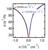
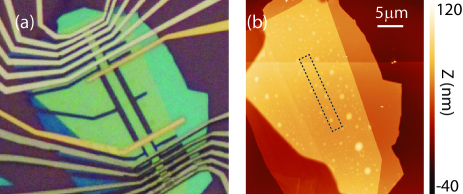
An optical image of device 1 after fabrication is shown in Fig. 1 (b). It is a two terminal hBN/Gr/hBN heterostructure with a large aspect ratio (length/width), which makes it ideal for magnetoconductance measurements. The conductivity as a function of charge carrier density is shown in Fig. 1 (c), from which we extract a mobility of and a residual doping of . At low temperature, phase coherent transport leads to weak localization as shown in Fig. 1 (d). Here, we plot an ensemble averaged quantum correction to the magneto conductivity at different temperatures, which we obtain by subtracting the classical magneto conductivtiy measured at from the low temperature measurements. The quantum correction to the magnetoconductivity can be fitted by the standard weak localization (WL) formula for grapheneMcCann et al. (2006):
| (1) |
where , with being the digamma function, , where is the diffusion constant, the phase coherence time, the intervalley scattering time and the intravalley scattering time. We fit the curves corresponding to the three different temperatures within the same fitting procedure (global fit), where only is allowed to change with temperature to extract all relevant scattering time scalesTikhonenko et al. (2008). We generally find phase coherence times on the order of a few pico seconds at a temperature of a few Kelvins and an intervalley scattering time of and very small intravalley scattering times . Whereas the extraction of inter and intravalley scattering times might be challenging in certain cases, the phase coherence time can be reliably extracted in all cases since it is given by the curvature of the magnetoconductivty at zero out-of-plane magnetic field.
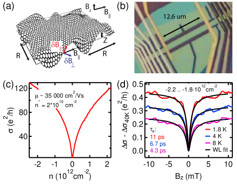
In order to probe the out-of-plane corrugations we study phase coherent transport as a function of small out-of-plane magnetic fields in the presence of large, static in-plane magnetic fields. It is obvious that a homogeneous in-plane magnetic field leads to random out-of-plane components if the graphene sheet has out-of-plane corrugations, see Fig. 1 (a). These random out-of-plane magnetic field components can be described as random vector potentials that affects phase coherent transport.
First experiments have been realized on Si inversion layersMensz et al. (1987); Anderson et al. (1993) and two-dimensional electron gases in GaAs-heterojunctionsMensz et al. (1987). A direct correlation between the topographic morphology and the dephasing rate has been found. Motivated by these findings, Mathur and Baranger have calculated the additional dephasing for a two-dimensional electron gas originating from Gaussian correlated corrugations in the presence of an in-plane magnetic fieldMathur and Baranger (2001):
| (2) |
Here, is the root-mean-square of the corrugation height, the lateral correlation length of the corrugations, is the in-plane magnetic field, the Fermi velocity and constants and are the electronic charge and the reduced Planck constant respectively.
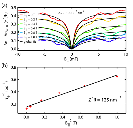
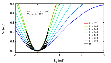
The quantum correction to the magnetoconductivity for different in-plane magnetic fields is shown in Fig.2 (a). Here we show a representative data set for hole doping. Single WL curves represent an ensemble averaged measurement over a density range of . Similar effects have been observed for electron doping. Different colours represent WL curves measured at different in-plane magnetic fields. As the in-plane field increases, the dip around zero magnetic field gets less pronounced and the overall magnetoconductance reduces. This changes can be understood by a reduced phase coherence time .
In order to perform a quantitative analysis, we apply a global fit (fitting all the curves with different at the same time) where only is allowed to vary since neither nor are expected to be affected by . The extracted dephasing rate is shown in Fig. 2 (b) as a function of . A clear linear behaviour is observed that allows us to extract the corrugation volume using Eq. 2. The relatively large corrugation volume, which is much larger than the previously reported value of for graphene on SiO2 Lundeberg and Folk (2010), can be explained by the presence of bubbles in the device. Bubbles with contaminations are known to spontaneously form at interfaces of vdW heterostructures Haigh et al. (2012); Kretinin et al. (2014) and were confirmed by optical and AFM images of device 1. Therefore, it is not surprising that an additional dephasing is observed when device 1 is placed in an in-plane magnetic field.
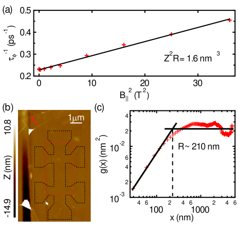
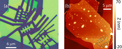
However, we also found an additional dephasing in much cleaner and essentially bubble free hBN/Gr/hBN heterostructures. We have measured the phase coherence time as a function of in-plane magnetic field . Here we directly show in Fig. 3 (a) the extracted dephasing rate as a function of of device 2 at a doping of . The dephasing rate was extracted from the curvature of the magnetoconductivity at zero out-of-plane magnetic field, see Fig. 5 in appendix B for more details. This device, which is free from bubbles (confirmed by AFM measurements, see Fig. 3 (b)), shows a corrugation volume . This is two orders of magnitude smaller than the extracted volume for device 1 that contains bubbles and surprisingly close to the corrugation volume of graphene on SiO2.
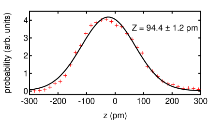
The additional dephasing in an in-plane magnetic field only gives access to the total corrugation volume and not to the individual contributions of height and radius . We used high resolution AFM images to extract the standard deviation of a Gaussian height distribution that corresponds to the corrugation height and the height-height correlation length that corresponds to the corrugation radius . An AFM image of device 2, with the outline of the Hall bar, before placing the top hBN, is shown in Fig. 3 (b)(see appendix for further fabrication details). From the height distribution, we extracted =, see Fig. 9 in appendix C. In addition, the same dataset is used to extract the height-height correlation length, which is the characteristic length scale for the corrugations. As shown in Fig. 3 (c), the correlation length corresponds to the crossover between the small and large length scale behaviour of the correlation function as evident in a log-log plot. We find for this device. Analysis of further graphene/hBN half-stacks prepared in the same manner, revealed very similar values for the height distribution and lateral correlation length. Thus, we find a corrugation volume by analysing AFM images . This independent rough estimation of the corrugation volume matches the corrugation volume extracted from transport measurements well.
Even though graphene is sandwiched between two layers of atomically flat hBN crystals, out-of-plane corrugations are present. The corrugation volume in bubble free hBN encapsulated graphene () is similar to the corrugation volume of SiO2 supported graphene (). However, in the case of hBN encapsulated graphene, the corrugations have a smaller height but larger lateral extension compared to the relatively short length scales in graphene on SiO2, which is on the order of a few nanometers Lundeberg and Folk (2010); Ishigami et al. (2007).
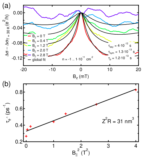
Out-of-plane corrugations are not limited to hBN encapsulated graphene, but are a generic phenomena in vdW-hetersotructures. Here we present phase coherent transport in hBN/Gr/WSe2 heterostructures, where additional dephasing is observed when an in-plane magnetic field is applied. Fig. 4 (a) shows the quantum correction of the magneto conductivity that exhibits weak anti-localization (WAL) due to graphene’s proximity to the TMDC WSe2 Zihlmann et al. (2018). In the case of graphene, the quantum correction to the magneto conductivity in the presence of strong SOC is given by McCann and Fal’ko (2012):
| (3) |
where , with being the digamma function, , where is the diffusion constant, the phase coherence time, () the spin-orbit scattering time that takes only spin-orbit terms into account that are asymmetric (symmetric) in direction. Assuming that and are independent of , we perform a global fit where only is allowed to vary with . We have also varied the spin orbit times, which did essentially not change within the limits of the extraction method, see also Ref. Zihlmann et al., 2018 for further information. The extracted dephasing rate scales linearly as a function of as shown in Fig. 4 (b). Using equation 2, a corrugation volume is extracted. This is roughly an order of magnitude smaller (larger) than in device 1 (2).
III Discussion
Despite the fact that hBN crystals are atomically flat and of high quality, graphene encapsulated between two such crystals exhibits out-of-plane corrugations. The corrugation volume extracted from phase coherent transport measurements varies among different vdW heterostructures depending on their interface and crystal quality. The large corrugation volume observed in device 1 is obviously originating from bubbles at the Gr/hBN interface and can be avoided by utilizing heterostructures with a better interface quality or by designing the active area of the device in a bubble free part of the heterostructure. However, in essentially bubble free heterostructures, out-of-plane corrugations are still present. Whereas for device 3 the vdW-interface might still be the limiting factor in terms of origin of out-of-plane corrugations, this is certainly not the case in device 2 where AFM images show a smooth, atomically flat surface without any bubbles or contaminations. Here, a different explanation for the presence of out-of-plane corrugations has to be invoked. One possibility is that the crystal quality of hBN might influence the remaining out-of-plane corrugations since defects in the hBN crystal (also in layers far away from the interface to the graphene) might lead to long-range height fluctuationsRooney et al. (2017). Moreover, residues trapped at the bottom hBN - SiO2 interface might lead to long range height fluctuations at the top of the bottom hBN.
Our results are in agreement with previous measurements on graphene on SiO2 substrate (Lundeberg and Folk, 2010). It is clear that devices with bubbles exhibit a larger corrugation volume than devices on a clean SiO2 surface. However, it is surprising that not even the best hBN/Gr/hBN devices show a smaller corrugation volume than devices on SiO2 substrates. It is important to note, that even though the corrugation volume is similar, the lateral correlation length is much longer and the height variation is considerably smaller for vdW heterostructures ( , ) compared to a SiO2 substrate ( , Geringer et al. (2009); Cullen et al. (2010)). Therefore, the deformations of the graphene lattice and hence the random strain fluctuations are greatly reduced in graphene in vdW-heterostructures compared to graphene on SiO2 substrates. This might be one of the reasons why the graphene quality in fully encapsulated graphene can be exceptionally good.
Finally, we would like to raise the point that the presence of out-of-plane corrugations (even in the cleanest devices) might impose severe limitations on phase coherent experiments relying on large in-plane magnetic fields. This for example prevents one from studying the transition from WAL to WL in graphene with spin-orbit coupling triggered by an in-plane magnetic field McCann and Fal’ko (2012); Zihlmann et al. (2018). In addition, the magnitude of the supercurrent in a graphene based Josephson junction in an in-plane magnetic field could be reduced due to a reduced phase coherence time.
IV Conclusion
In conclusion, phase coherent transport has shown that out-of-plane corrugations are present in vdW-heterostructures. The corrugation volume strongly depends on the interface quality between graphene and other 2D-material (e.g. hBN and WSe2) but is non-zero even for the best interface and device quality ( ). The presence of out-of-plane corrugations implies distortions of the graphene lattice and hence also random strain fluctuations. While the corrugation volume for the cleanest hBN/Gr/hBN device is similar to graphene on SiO2, its effect on transport is greatly reduced because of the long range nature of the corrugations in hBN/Gr/hBN (smaller strain fluctuations). Nonetheless, phase coherent experiments relying on large in-plane magnetic fields could suffer from the out-of-plane corrugations due to a reduced phase coherence time.
Acknowledgements.
This work has received funding from the European Union’s Horizon 2020 research and innovation programme under grant agreement 696656 (Graphene Flagship), 787414 (ERC-Adv TopSupra), and 824109 (European Microkelvin Platform EMP); the Swiss National Science Foundation (including 179024); the Swiss Nanoscience Institute; the Swiss NCCR QSIT; and Topograph FlagERA network OTKA FK-123894. This research was supported by the National Research, Development and Innovation Fund of Hungary within the Quantum Technology National Excellence Program (Project Nr. 2017-1.2.1-NKP-2017-00001). P.M. acknowledges support from the Marie Curie and Bolyai fellowships. K.W. and T.T. acknowledge support from the Elemental Strategy Initiative conducted by the MEXT, Japan ,Grant Number JPMXP0112101001, JSPS KAKENHI Grant Numbers JP20H00354 and the CREST(JPMJCR15F3), JST.Author contributions
Devices were fabricated by S.Z., M.K.R, D.I. and M.K. Measurements were performed by S.Z. and M.K.R with the help of P.M.. S.Z. and M.K.R. analysed the data with help from P.M. and inputs from C.S. and D.M.Z.. S.Z., P.M., L.W., D.I. and C.S. were involved in the interpretation of the results. S.Z. and P.M. co-wrote the manuscript with inputs from all authors. D.M.Z, C.S. and P.M. guided the work. K.W. and T.T. provided the hBN crystals used in the devices.
Appendix A Overview of the measured devices
Table 1 shows an overview of the three devices.
| cm2/Vs | 1012cm-2 | m2/s | |||||||
|---|---|---|---|---|---|---|---|---|---|
| device 1 | -2.2..-1.8 | 0.32 | 640 | 8 | 1.6 | na | |||
| hBN/Gr/hBN | |||||||||
| device 2 | 0.3..1.2 | 0.23 | 460 | 4.3 | |||||
| hBN/Gr/hBN | |||||||||
| device 3 | -0.1..0.1 | 0.075 | 150 | 3.8 | 0.53 | na | |||
| WSe2/Gr/hBN |
Fabrication of device 1 and device 3
The vdW-heterostructures of device 1 and device 3 were assembled using a dry pick-up method Zomer et al. (2014) and Cr/Au 1D-edge contacts were usedWang et al. (2013). After shaping the vdW-heterostructure into a Hall-bar geometry by a reactive ion etching plasma employing SF6 as the main reactive gas, Ti/Au top gates with an MgO dielectric layer were fabricated on device 3. A heavily-doped silicon substrate with SiO2 was used as a global back gate for both devices.
Fabrication of device 2
Device 2 was not fabricated using the dry pick-up method but relying on a wet process where the graphene is transferred by a PMMA membrane on a hBN flake Dean et al. (2010). After PMMA removal in acetone, the sample was annealed at in a hydrogen atmosphere (). Clean and wrinkle-free areas were identified imaging the the heterostructure by non-contact AFM prior to the deposition of a top hBN layer to protect the graphene from further fabrication steps. These AFM images were also used to extract the data shown in Fig. 3. The deposition of the top hBN could in principle induce additional corrugation. However, The device shaping as well as the contact deposition was performed in the same way as for device 1 and device 3.
Measurements
Standard low frequency lock-in techniques were used to measure two- and four-terminal conductances and resistances. Weak (anti-)localization was measured at a temperature of whereas a classical background was measured at sufficiently large temperatures of for device 1 and device 3. Device 2 was measured at and no classical background was subtracted. A vector magnet was used to independently control the in-plane () and out-of-plane () magnetic field component.
The quantum correction to the magnetoconductivity was only analysed in the interval , where is the so-called transport field that describes the limit of diffusive transport.
The diffusion constant was calculated in the following way:
| (4) |
where is the reduced Planck constant, the Fermi velocity of graphene, and the fundamental unit of charge. The conductivity was measured and was calculated from a parallel plate capacitor model. The residual doping, , was used as a cut-off to calculate around the charge neutrality point.
Appendix B Magneto conductivity of device 2
Instead of fitting the full WL formula 1 to the magneto conductivity, the phase coherence time can also be extracted from the curvature of the magnetoconductance () at zero out-of-plane magnetic field () Lara-Avila et al. (2015):
| (5) |
where is the diffusion constant, is the phase coherence time and the constants and are the electron’s charge and Planck’s constant respectively. This is especially useful for very high mobility devices where is very small. Fig. 5 shows the magneto conductivity for electron doping for various in-plane magnetic fields. It is clearly observable that the curvature at zero gets smaller for larger in-plane magnetic field, hence the phase coherence time is smaller as well.
Appendix C Additional information on the AFM analysis
The AFM analysis presented in the main text and below has been performed on device 2 before placing the top hBN. The area marked by the red dashed rectangle shown in Fig. 3 (b), which corresponds to the area where the Hall bar has been defined, was used to extract and . Therefore, the AFM analysis and the transport measurements probe the same area. A tilted plane has been subtracted from the height data prior to the detailed analysis described in the following.
The rms height () of the corrugations can directly be extracted from AFM measurements by either calculating it from the raw data (point by point) or by fitting the height distribution with a Gaussian model. The point by point calculation of is given as:
| (6) |
where is the height value of point and is the average height value of all points of the AFM image. Additionally, the height distribution as shown in Fig. 9, can be used to extract . We find = from the width of the height distribution, which is in good agreement with literature values for graphene on hBNDean et al. (2010).
The height-height correlation function in one dimension Ishigami et al. (2007) is defined as follows for a discrete dataset:
| (7) |
where and is the spacing between two points. Eq. 7 represents the 1-dimensional height-height correlation function averaged over lines of the second lateral dimension as commonly used in the analysis of AFM images, where is calculated for the fast scanning directions and averaged over the slow scanning direction. Eq. 7 has been used to calculate , which is shown in Fig. 3 (c) in the main text. The correlation length is identified as the crossover from the polynomial short range behaviour to the constant long range behaviour.
For a Gaussian correlated surface, as assumed by Mathur and BarangarMathur and Baranger (2001) for their calculation, the height-height correlation function takes the form:
| (8) |
where is the root mean square deviation from the mean height and is the correlation length. This is a direct result of the assumption of a Gaussian correlated surface that is defined by a height distribution with zero mean and a variance given by
| (9) |
where and are positions along the x-direction, is the rms height fluctuation and is the correlation length.
The crossover between the short range behaviour and the long range behaviour takes place at , as indicated by the crossing of the black dashed lines in Fig. 3(c) in the main text. In addition, the value for the long range behaviour ( as given by eq. 8 for large, uncorrelated distances) agrees well with extracted from the height distribution. Fitting the data with eq. 8 results in and , which gives a reasonable agreement with the general calculation.
We would like to note that the corrugation volume extracted from transport measurements can directly be compared to the corrugation volume extracted from AFM measurements, see Ref. Mathur and Baranger, 2001; Anderson et al., 1993; Minkov et al., 2004 for further information. In order that eq. 2 is valid, it is assumed that the correlation length () is of short range compared to the mean free path Mathur and Baranger (2001). This condition is fulfilled for device 2 where the correlation length has been determined by AFM measurements. It is a question whether this condition is valid for device 1 and 3. However, the experimental finding () suggests also a homogeneous broadening described by eq. 2.
References
- Peierls (1934) Rudolf Peierls, “Bemerkungen über umwandlungstemperaturen,” Helvetica Physica Acta 7 (1934).
- Peierls (1935) Rudolf Peierls, “Quelques propriétés typiques des corps solides,” Annales de l’institut Henri Poincaré 5, 177–222 (1935).
- Landau (1937) L. D. Landau, “Zur theorie der phasenumwandlungen ii,” Phys. Z. Sowjetunion 11, 26–35 (1937).
- Mermin (1968) N. D. Mermin, “Crystalline order in two dimensions,” Phys. Rev. 176, 250–254 (1968).
- Novoselov et al. (2004) K. S. Novoselov, A. K. Geim, S. V. Morozov, D. Jiang, Y. Zhang, S. V. Dubonos, I. V. Grigorieva, and A. A. Firsov, “Electric Field Effect in Atomically Thin Carbon Films,” Science 306, 666–669 (2004), http://www.sciencemag.org/content/306/5696/666.full.pdf .
- Novoselov et al. (2005) K. S. Novoselov, D. Jiang, F. Schedin, T. J. Booth, V. V. Khotkevich, S. V. Morozov, and A. K. Geim, “Two-dimensional atomic crystals,” Proceedings of the National Academy of Sciences of the United States of America 102, 10451–10453 (2005), http://www.pnas.org/content/102/30/10451.full.pdf .
- Meyer et al. (2007) Jannik C. Meyer, A. K. Geim, M. I. Katsnelson, K. S. Novoselov, T. J. Booth, and S. Roth, “The structure of suspended graphene sheets,” Nature 446, 60–63 (2007).
- Fasolino et al. (2007) A. Fasolino, J. H. Los, and M. I. Katsnelson, “Intrinsic ripples in graphene,” Nature Materials 6, 858–861 (2007).
- Ishigami et al. (2007) Masa Ishigami, J. H. Chen, W. G. Cullen, M. S. Fuhrer, and E. D. Williams, “Atomic structure of graphene on sio2,” Nano Lett. 7, 1643–1648 (2007).
- Lui et al. (2009) Chun Hung Lui, Li Liu, Kin Fai Mak, George W. Flynn, and Tony F. Heinz, “Ultraflat graphene,” Nature 462, 339–341 (2009).
- Geringer et al. (2009) V. Geringer, M. Liebmann, T. Echtermeyer, S. Runte, M. Schmidt, R. Rückamp, M. C. Lemme, and M. Morgenstern, “Intrinsic and extrinsic corrugation of monolayer graphene deposited on ,” Phys. Rev. Lett. 102, 076102 (2009).
- Cullen et al. (2010) W. G. Cullen, M. Yamamoto, K. M. Burson, J. H. Chen, C. Jang, L. Li, M. S. Fuhrer, and E. D. Williams, “High-fidelity conformation of graphene to topographic features,” Phys. Rev. Lett. 105, 215504 (2010).
- Katsnelson and Geim (2008) M. I. Katsnelson and A. K. Geim, “Electron scattering on microscopic corrugations in graphene,” Philosophical Transactions of the Royal Society A: Mathematical, Physical and Engineering Sciences 366 (2008).
- Couto et al. (2014) Nuno J. G. Couto, Davide Costanzo, Stephan Engels, Dong-Keun Ki, Kenji Watanabe, Takashi Taniguchi, Christoph Stampfer, Francisco Guinea, and Alberto F. Morpurgo, “Random Strain Fluctuations as Dominant Disorder Source for High-Quality On-Substrate Graphene Devices,” Phys. Rev. X 4, 041019 (2014).
- Kim et al. (2019) Youngwook Kim, Patrick Herlinger, Takashi Taniguchi, Kenji Watanabe, and Jurgen H. Smet, “Reliable postprocessing improvement of van der waals heterostructures,” ACS Nano 13, 14182–14190 (2019).
- Wang et al. (2019) Lujun Wang, Péter Makk, Simon Zihlmann, Andreas Baumgartner, David I. Indolese, Kenji Watanabe, Takashi Taniguchi, and Christian Schönenberger, “Mobility enhancement in graphene by in situ reduction of random strain fluctuations,” (2019), arXiv:1909.13484 .
- Lundeberg and Folk (2010) Mark B. Lundeberg and Joshua A. Folk, “Rippled Graphene in an In-Plane Magnetic Field: Effects of a Random Vector Potential,” Phys. Rev. Lett. 105, 146804 (2010).
- Dean et al. (2010) C. R. Dean, A. F. Young, I. Meric, C. Lee, L. Wang, S. Sorgenfrei, K. Watanabe, T. Taniguchi, P. Kim, K. L. Shepard, and J. Hone, “Boron nitride substrates for high-quality graphene electronics,” Nat Nano 5, 722–726 (2010).
- Wang et al. (2013) L. Wang, I. Meric, P. Y. Huang, Q. Gao, Y. Gao, H. Tran, T. Taniguchi, K. Watanabe, L. M. Campos, D. A. Muller, J. Guo, P. Kim, J. Hone, K. L. Shepard, and C. R. Dean, “One-Dimensional Electrical Contact to a Two-Dimensional Material,” Science 342, 614–617 (2013), http://science.sciencemag.org/content/342/6158/614.full.pdf .
- Kretinin et al. (2014) A. V. Kretinin, Y. Cao, J. S. Tu, G. L. Yu, R. Jalil, K. S. Novoselov, S. J. Haigh, A. Gholinia, A. Mishchenko, M. Lozada, T. Georgiou, C. R. Woods, F. Withers, P. Blake, G. Eda, A. Wirsig, C. Hucho, K. Watanabe, T. Taniguchi, A. K. Geim, and R. V. Gorbachev, “Electronic properties of graphene encapsulated with different two-dimensional atomic crystals,” Nano Lett. 14, 3270–3276 (2014).
- Lu et al. (2014) Chih-Pin Lu, Guohong Li, K. Watanabe, T. Taniguchi, and Eva Y. Andrei, “: Choice substrate for accessing and tuning the electronic properties of graphene,” Phys. Rev. Lett. 113, 156804 (2014).
- Banszerus et al. (2017) L Banszerus, H Janssen, M Otto, A Epping, T Taniguchi, K Watanabe, B Beschoten, D Neumaier, and C Stampfer, “Identifying suitable substrates for high-quality graphene-based heterostructures,” 2D Materials 4, 025030 (2017).
- Zihlmann et al. (2018) Simon Zihlmann, Aron W. Cummings, Jose H. Garcia, Máté Kedves, Kenji Watanabe, Takashi Taniguchi, Christian Schönenberger, and Péter Makk, “Large spin relaxation anisotropy and valley-Zeeman spin-orbit coupling in /graphene/-BN heterostructures,” Phys. Rev. B 97, 075434 (2018).
- Banszerus et al. (2019) L. Banszerus, T. Sohier, A. Epping, F. Winkler, F. Libisch, F. Haupt, K. Watanabe, T. Taniguchi, K. Müller-Caspary, N. Marzari, F. Mauri, B. Beschoten, and C. Stampfer, “Extraordinary high room-temperature carrier mobility in graphene-wse2 heterostructures,” (2019), arXiv:1909.09523 .
- Engels et al. (2014) S. Engels, B. Terrés, A. Epping, T. Khodkov, K. Watanabe, T. Taniguchi, B. Beschoten, and C. Stampfer, “Limitations to carrier mobility and phase-coherent transport in bilayer graphene,” Phys. Rev. Lett. 113, 126801 (2014).
- Mathur and Baranger (2001) H. Mathur and Harold U. Baranger, “Random berry phase magnetoresistance as a probe of interface roughness in si mosfet’s,” Phys. Rev. B 64, 235325 (2001).
- McCann et al. (2006) E. McCann, K. Kechedzhi, Vladimir I. Fal’ko, H. Suzuura, T. Ando, and B. L. Altshuler, “Weak-Localization Magnetoresistance and Valley Symmetry in Graphene,” Phys. Rev. Lett. 97, 146805 (2006).
- Tikhonenko et al. (2008) F. V. Tikhonenko, D. W. Horsell, R. V. Gorbachev, and A. K. Savchenko, “Weak Localization in Graphene Flakes,” Phys. Rev. Lett. 100, 056802 (2008).
- Mensz et al. (1987) P. M. Mensz, R. G. Wheeler, C. T. Foxon, and J. J. Harris, “Determination of spatial potential fluctuations in si and gaas inversion layers by weak localization,” Applied Physics Letters 50, 603–605 (1987), https://doi.org/10.1063/1.98094 .
- Anderson et al. (1993) W. R. Anderson, D. R. Lombardi, R. G. Wheeler, and T. . Ma, “Determination of si/sio/sub 2/ interface roughness using weak localization,” IEEE Electron Device Letters 14, 351–353 (1993).
- Haigh et al. (2012) S. J. Haigh, A. Gholinia, R. Jalil, S. Romani, L. Britnell, D. C. Elias, K. S. Novoselov, L. A. Ponomarenko, A. K. Geim, and R. Gorbachev, “Cross-sectional imaging of individual layers and buried interfaces of graphene-based heterostructures and superlattices,” Nature Materials 11, 764–767 (2012).
- McCann and Fal’ko (2012) Edward McCann and Vladimir I. Fal’ko, “ Symmetry of Spin-Orbit Coupling and Weak Localization in Graphene,” Phys. Rev. Lett. 108, 166606 (2012).
- Rooney et al. (2017) Aidan. P. Rooney, Aleksey Kozikov, Alexander N. Rudenko, Eric Prestat, Matthew J. Hamer, Freddie Withers, Yang Cao, Kostya S. Novoselov, Mikhail I. Katsnelson, Roman Gorbachev, and Sarah J. Haigh, “Observing imperfection in atomic interfaces for van der waals heterostructures,” Nano Letters 17, 5222–5228 (2017).
- Zomer et al. (2014) P. J. Zomer, M. H. D. Guimarães, J. C. Brant, N. Tombros, and B. J. van Wees, “Fast pick up technique for high quality heterostructures of bilayer graphene and hexagonal boron nitride,” Applied Physics Letters 105, 013101 (2014), http://dx.doi.org/10.1063/1.4886096.
- Lara-Avila et al. (2015) Samuel Lara-Avila, Sergey Kubatkin, Oleksiy Kashuba, Joshua A. Folk, Silvia Lüscher, Rositza Yakimova, T. J. B. M. Janssen, Alexander Tzalenchuk, and Vladimir Fal’ko, “Influence of impurity spin dynamics on quantum transport in epitaxial graphene,” Phys. Rev. Lett. 115, 106602 (2015).
- Minkov et al. (2004) G. M. Minkov, O. E. Rut, A. V. Germanenko, A. A. Sherstobitov, B. N. Zvonkov, V. I. Shashkin, O. I. Khrykin, and D. O. Filatov, “Transverse negative magnetoresistance of two-dimensional structures in the presence of a strong in-plane magnetic field: Weak localization as a probe of interface roughness,” Phys. Rev. B 70, 035304 (2004).