CLICTD: A monolithic HR-CMOS sensor chip for the CLIC silicon tracker
Abstract:
The CLIC Tracker Detector (CLICTD) is a monolithic pixelated sensor chip produced in a nm imaging CMOS process built on a high-resistivity epitaxial layer. The chip, designed in the context of the CLIC tracking detector study, comprises a matrix of elongated pixels, each measuring . To ensure prompt charge collection, every elongated pixel is segmented in eight sub-pixels, each containing a collection diode and a separate analog front-end. A simultaneous -bit time measurement with ns time bins and -bit energy measurement with programmable range is performed in the on-pixel digital logic. The main design aspects as well as the first results from laboratory measurements with the CLICTD chip are presented.
[table]capposition=top
1 Introduction
A novel monolithic pixel sensor chip, the CLIC Tracker Detector (CLICTD), is presented. The CLICTD chip features a matrix of rows and columns with pixels of . The chip was designed according to the requirements for the silicon tracker at the future Compact Linear Collider (CLIC) [2]. These requirements include a Time of Arrival (ToA) measurement with ns time bins, and a -bit Time over Threshold (ToT) measurement for time walk correction. Moreover, the -bit ToT measurement (which has a programmable range from to ) enables a precise hit position interpolation that is needed to reach a single point resolution of along the transverse plane with the pitch of . Other requirements include a total material budget of X0 per detection layer (allowing for for the silicon layers) and an average power consumption below . In order to minimise the average analog power consumption, the analog front-end can be set to a standby power mode in the ms gaps between subsequent colliding bunch trains (power pulsing), taking advantage of the low duty cycle of the CLIC beam [3]. The digital power consumption is minimised by means of clock gating. Details on the CLICTD chip design have been presented in [4].
2 Process description
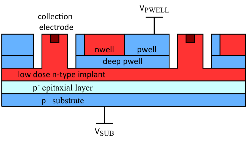
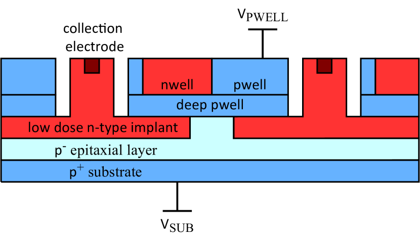
The design was implemented in a nm High-Resistivity (HR) CMOS imaging process, where a deep P-well is used in order to shield the on-pixel electronics from the collection electrode. The signal is collected with a small area N-well on top of a P-type high resistivity epitaxial layer. This results in a small capacitance (a few fF) for the collection electrode and helps to minimise the analog power consumption and the noise in the front-end. Full depletion of the epitaxial layer is achieved by including an additional deep N-type implant. Two different pixel layouts were implemented and manufactured through a process split on different wafers. As illustrated in Figure 1, the first pixel layout is with a continuous deep N-type implant, and the second with a segmented deep N-type implant to increase the lateral field and thereby reduce the charge collection time [5]. In addition, reduced charge sharing is expected because of the gap in the N-implant. The gap is introduced only along the long dimension of the pixel, as the short pixel dimension corresponds to the transverse detector plane, where charge sharing can be beneficial for improving the position resolution through hit position interpolation.
3 The CLICTD prototype chip
The CLICTD matrix comprises elongated pixels of . Each pixel is segmented in eight sub-pixels, each with its individual collection diode and analog front-end, to ensure prompt charge collection. The diodes are therefore spaced by along the long pixel direction. Every front-end includes level shifter, voltage amplifier, discriminator and a -bit local threshold tuning DAC. The level shifter acts as a unity gain buffer and is placed as close to the collection electrode as possible to minimise the input capacitance. One bit indicating whether the front-end detected a particle is stored for each sub-pixel, while the simultaneous -bit ToA and -bit ToT measurement is performed in the on-pixel digital logic for the combined output (by means of an ”OR” gate) of all eight discriminator outputs. Thus, the time-stamp of the first hit and the integral ToT of all hits within the same frame are read out for each pixel. A serial readout at MHz is employed. To reduce the amount of data shifted out of the chip, a compression algorithm is applied. The data acquired during the frame are shifted out only for pixels that detected a particle. For pixels that did not detect a particle, only one bit is shifted out.
4 Measurement results
Once fabricated, the CLICTD chip was characterised using the CaRIBOu readout system [6].
4.1 I-V characteristic
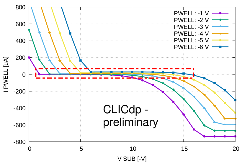
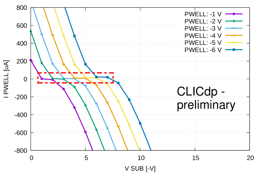
The sensor bias operation range was determined by measuring its I-V characteristics. The leakage current at the P-wells in the pixel area (biased at VPWELL in Figure 1) was measured, while scanning the substrate bias voltage, and for given values of the P-well bias ranging from to V. The region where the leakage current remains stable and relatively low ( for the full chip) is the region where the sensor can be operated (marked in red in Figure 2). For the first pixel layout in Figure 1(a), the continuous deep N-type implant offers a better isolation between the P-wells and the substrate. Therefore, the substrate can be biased to a higher (in absolute value) voltage, as shown in Figure 2(a). Due to the reduced isolation originating from the gap in the deep N-type implant in the second pixel layout, the sensor can be operated only when the two nodes are biased at a similar voltage level (Figure 2(b)), a result which is in agreement with simulations [5].
4.2 Noise measurements and equalisation
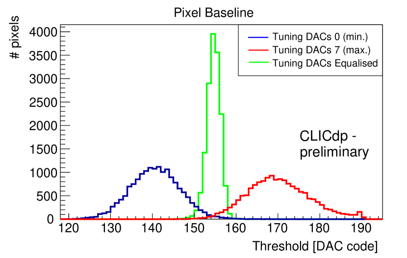
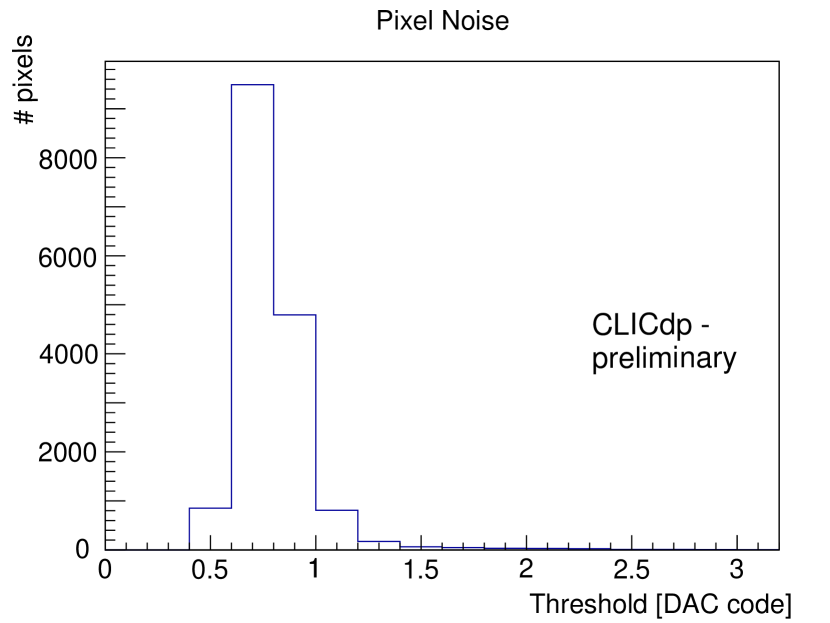
During the threshold equalisation for the CLICTD pixel matrix, the baseline for each sub-pixel is extracted as the mean value of the curve produced after scanning the threshold and counting the number of noise hits for each threshold. In order to equalise the matrix on a sub-pixel basis, the scan was performed for each of the eight sub-pixels in the pixel, while the rest of the sub-pixels were masked. The threshold scans were performed for the lowest and highest code of the -bit threshold tuning DAC in the front-end. A linear interpolation was applied in order to select the DAC codes for which the threshold dispersion over the matrix is minimised. Figure 3(a) presents the threshold scan for lowest (blue curve), highest (red curve) and equalised (green curve) DAC code. A histogram of the noise RMS per sub-pixel, extracted in threshold DAC codes as the RMS value of the curve resulting from the threshold scan for each sub-pixel, is plotted in Figure 3(b). Based on the threshold DAC step to electrons conversion extracted in Section 4.3, the threshold dispersion for the equalised CLICTD matrix is about e- and the mean value of the noise RMS is e-. The above results are from a CLICTD sample with gap in the n-layer, with both the P-wells and the substrate biased to V.
4.3 Measurements with radiation sources
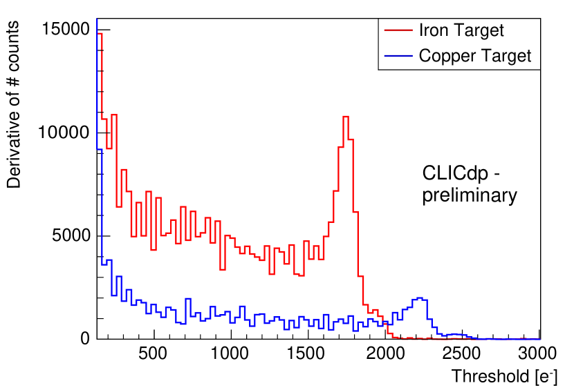
Figure 4(a) presents the fluorescence spectra from an iron (red curve) and a copper (blue curve) target, measured with the CLICTD chip using an X-ray beam. The CLICTD threshold was scanned during this measurement and the number of detected photons was stored in each pixel and read out for every threshold. The produced occupancy curve gives the number of counts above threshold, for each applied threshold step. For a given beam intensity and frame duration, this number depends on the fluorescence emission spectrum of the target. A differentiation of the occupancy curve gives the measured energy spectrum.
From the mean values of the Gaussian fits for the K peaks for iron ( keV) and copper ( keV), and with an electron-hole pair creation energy in silicon of eV, the LSB of the threshold DAC has been extracted to correspond to e-. The minimum detectable charge for the chip settings applied for this measurement is estimated to be e-.
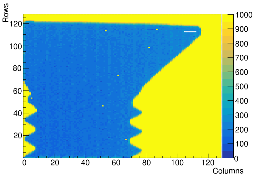
Using the same setup, an X-ray image of a small item (screw) was taken with the CLICTD chip. The image presented in Figure 4(b) was produced with acquisitions of shutter length, with equalised matrix. The number of frames when a hit was detected is plotted for each sub-pixel.
For the above measurements, a CLICTD sample with continuous N-implant was used, while the reverse bias was set to V at the P-wells and to V at the substrate. The sensor capacitance (and consequently the front-end performance) strongly depends on the sensor bias [7]. The front-end was biased at its default values after chip reset and the operation parameters were not yet tuned for signal-to-noise performance. Under these bias conditions, the analog part of the matrix consumes , while the on-pixel digital logic consumes another . The expected average power consumption of the CLICTD matrix over the cycle of the CLIC accelerator, as extrapolated from static power measurements and simulated values, is , after applying the power pulsing scheme introduced in Section 1. In addition, are consumed by the analog and digital periphery electronics.
5 Summary
A monolithic sensor chip, the CLIC Tracker Detector (CLICTD), designed in the framework of the CLIC silicon tracker study, has been presented. The chip was produced in a modified CMOS imaging process and features a novel architecture with segmented pixels. Preliminary results show a threshold dispersion of e- and a mean noise RMS of e- over the CLICTD matrix, after threshold equalisation. The average power consumption over the CLIC beam cycle is estimated to be for the pixel matrix, plus for the periphery electronics.
Acknowledgements
This project has received funding from the European Union’s Horizon 2020 research and innovation programme under grant agreement No 654168.
References
- [1]
- [2] D. Dannheim, A. Nurnberg, Requirements for the CLIC tracker readout, CLICdp-Note-2017-002. 2017.
-
[3]
Physics and Detectors at CLIC: CLIC Conceptual Design Report,
edited by L. Linssen, A. Miyamoto, M. Stanitzki, H. Weerts, CERN-2012-003. 2012. - [4] I. Kremastiotis et al., Design of a monolithic HR-CMOS sensor chip for the CLIC silicon tracker, CLICdp-Conf-2018-008. 2018.
- [5] M. Munker et al., Simulations of CMOS pixel sensors with a small collection electrode, improved for a faster charge collection and increased radiation tolerance, JINST 14 C05013. 2019.
- [6] A. Fiergolski, A multi-chip data acquisition system based on a heterogeneous system-on-chip platform, CLICdp-Conf-2017-012. 2017.
- [7] M. Munker, Test beam and simulation studies on High Resistivity CMOS pixel sensors, CERN-THESIS-2018-202. 2018.
- [8]