Interface Dark Excitons at Sharp Lateral Two-Dimensional Heterostructures
Abstract
We study the dark excitons at the interface of a sharp lateral heterostructure of two-dimensional transition metal dichalcogenides (TMDs). By introducing a low-energy effective Hamiltonian model, we find the energy dispersion relation of exciton and show how it depends on the onsite energy of composed materials and their spin-orbit coupling strengths. It is shown that the effect of the geometrical structure of the interface, as a deformation gauge field (pseudo-spin-orbit coupling), should be considered in calculating the binding energy of exciton. By discretization of the real-space version of the dispersion relation on a triangular lattice, we show that the binding energy of exciton depends on its distance from the interface line. For exciton near the interface, the binding energy is equal to 0.36 eV, while for the exciton far enough from the interface, it is equal to 0.26 eV. Also, it has been shown that for a zigzag interface the binding energy increases by 0.34 meV compared to an armchair interface due to the pseudo-spin-orbit interaction (gauge filed). The results can be used for designing 2D-dimensional-lateral-heterostructure- based optoelectronic devices to improve their characteristics.
pacs:
73.63.-b, 71.35 Cc, 71.70.EjI Introduction
Direct band gap semiconductors are one of the main candidates of photon absorption or emission. If the energy of photons be equal or greater than the energy band gap of the semiconductors they will excite the electrons from valence band to the conduction band. Also, the photons will be emitted by coming back the excited electrons to the valence band. By adding the n (p)-type impurities to semiconductors new energy levels are created near the conduction (valence) band edge inside the band gap of semiconductors. The electrons and holes can be exited to the new energy levels in photon absorption process or coming back to the valence band in photon emission process. Another mechanism for creating an energy level inside the band gap is the creation of exciton. An exciton can be created by coupling an electron with a hole. If the spin of electron and hole be not (be) same a dark (bright) ecxiton is created. Also, by absorption of photons near the junction area of a reversed bias pn-junction the created electrons (holes) will be injected to the n (p)-region and in consequence a photocurrent is created. If the band gap of the semiconductor be small, such as Indium Antimonite (InSb), the device should be cooled to very low temperature. Therefore, the direct or indirect type of band gap, the value of the band gap, the working temperature of device and the creation of energy levels in the band gap by adding the impurities or creation of exciton are important factors in designing the optoelectronic devices.
A homojunction can be created by doping an impurity in a semiconductor material with specific band gap energy. The interface of two dissimilar semiconductors forms a heterojunction. The combination of multiple heterojunctions together in a device is called heterostructure. The semiconductors band alignment in heterojunctions can be categorized into three different types. In type I (straddling gap), the conduction band minimum (CBM) of one material is contained (nested) inside the band gap of other material. If the band-gap of one material is rested inside the band gap of the other material, the type II alignment (staggered gap) is formed. In type III (broken gap), the CBM of one material is equal to the valence band maximum (VBM) of the other material. Therefore, the different types of heterostructures can be created by using the heterojunctions and the band gap engineering technique. The new heterostructures can be considered as new candidate for designing the optoelectronic devices.
Recently, two dimensional materials (2DMs) have been considered as the new candidate for manufacturing heterostructurs. Different two-dimensional materials with honeycomb structures have been investigated. Hexagonal boron nitride (h-BN) Lin, Williams, and Connell (2010); Weng et al. (2016), transition metal dichalcogenides (TMDs) Lv et al. (2015); Tan and Zhang (2015), black phosphorus (BP) Liu et al. (2015); Chen et al. (2018) and silicene Kara et al. (2012) are the most widely studied 2DMs. By vertical (vertical heterostructures (VHSs)) or lateral (lateral heterostructures (LHSs)) integration of 2DMs, an artificial heterostructured 2D layer can be fabricated. The single-, double-, and multi-step chemical vapor deposition (CVD) approaches have been used to grow large -area, sharp 2D heterostructures Duan et al. (2014a); Heo et al. (2015); Gong et al. (2015); Zhang et al. (2017). Also, using the techniques, researchers could grow hetero-triangles composed of a central TMD and an outer triangular ring of another TMD Duan et al. (2014a); Huang et al. (2014); Gong et al. (2014). The other structures such as truncated triangles, hexagons, hexagrams Zhang et al. (2015a) and more complex patterned structures have also been reported Mahjouri-Samani et al. (2015).
The built-in potential in pn-junction and its increasing rate under the reversed bias condition are important parameters in designing the homojundtion-based optoelectronic devices. Similarly, the band alignment (or band offset) across the junction is an important parameter in material design. The band offset in VHSs Gong et al. (2013); Kosmider and Rossier (2017) and in LHSs Kang et al. (2013) have been studied by using the density functional theory (DFT). Ozcelik et al., have introduced the periodic table of heterostructures (HSs) based on the band offset between them Ozcelik et al. (2016). For studying the properties of HSs the tight-binding approach has been used for not only commensurate HSs Zhang et al. (2016); Avalos-Ovando, Mastrogiuseppe, and Ulloa (2019) but also for incommensurate types Choukroun et al. (2019).
Different types of devices can be designed and manufactured after acquisition of design and manufacturing technologies of two dimensional Heterostures (2DHSs). For example, by using monolayer WSe2-WS2 HS, high mobility field-effect transistors (FETs), complementary metal-oxide semiconductor (CMOS) and superior photovoltaic devices have been demonstrated Duan et al. (2014b). A light-emitting device (LED) with large conversion efficiency has been built by using the lateral WSe2-MoS2 HS Li et al. (2018). It has been shown that one can manufacture a photodiode with high photodetectivity of Jones and short response time of sub- by using the LHS of graphene and thin amorphous carbon Chen et al. (2019). Amani et al., have reported near-unity photon quantum yield in TMD monolayer, which led to the development of highly efficient optoelectronic devices Amani et al. (2015). It has been shown that Mo- and W-based TMDs have bright and dark exciton ground states, respectively, due to the reversal of spins in the conduction band Godde et al. (2016); Zhang et al. (2015b).
As it has been mentioned above, exciton energy level is placed inside the energy band gap region. Therefore, the creation of exciton in 2DHSs is important from the 2DHS-based optoelectronic devices point of view. The long-lived interlayer excitons in monolayer MoSe2-WSe2 HS have been reported Rivera, Yao, and et al. (2015), and the light-induced exciton spin Hall effect in van der Waals HSs has been studied Li et al. (2015). Latini et al., have studied the role of the dielectric screening on the properties of excitons in van der Waals HSs Latini, Olsen, and Thygesen (2015). Lau et al., have studied the interface excitons at lateral heterojunctions in monolayer semiconductors and shown that the competition between the lattice and Coulomb potentials implies the properties of exciton at the interface Lau et al. (2018).
One of the important properties of 2DMs is the effect of its boundary on the electronic properties of the nanoribbons composed by the materials. Therefore, it is expected that by changing the electronic property of the nanoribbons, due to the change in their boundaries, the photon absorption and emission by the nanoribbons change, too. It means that in addition to the previous important parameters, the boundary condition or the geometry of two-dimensional nanoribbons be another important parameter in designing and manufacturing the 2DHS-basde optoelectronic devices. For example, it has been shown that the plane integrated modular wave functions of the VBM and CBM for different LHSs with long armchair and zigzag interfaces are localized on Mo-side and W-side, respectively Jin et al. (2019). Also, it has been shown that the wave function behavior is quite different in LHSs with zigzag interface compared to armchair interfaceJin et al. (2019).For studying the effect of geometry on the wave function, the normal derivative is substituted by the covariant derivative. It is done by introducing a deformation gauge filed which is subtracted from the momentum operate in the Hamiltonian of the systemJin et al. (2019).
The above short review shows that band gap energy, band offset voltage, type of alignment, interface structure, and the type of chalcogenide in the lateral MiXj-MkXl (M=transition metal, X=chalcogenide) heterostructures are important in designing an exciton-based optoelectronic devices. The importance of these factors motivated us to study the relationship between the energy of exciton, its binding energy, and the mentioned parameters in the LHSs.
In this paper, we consider monolayer LHSs of transition metal dichalcogenide with armchair and zigzag interfaces. By introducing a low-energy effective Hamiltonian model,we find the energy dispersion relation of dark exciton and show how it depends on the onsite energy of composed materials and their spin-orbit coupling strengths. Using the real-space version of exciton dispersion energy relation and its discretizing on a triangular lattice we find the binding energy of exciton. It is shown that the binding energy depends on the distance of the exciton from the interface line which is governed by the competition between lattice and Coulomb potentials. We show that the effect of the geometrical structure of the interface appears as a deformation gauge field and increases the binding energy of exciton in the zigzag interface. The structure of the article is as follows: Section II includes the Hamiltonian model. The numerical calculations are provided in section III. The results and discussion and summary are provided in sections IV and V, respectively.
II Hamiltonian model
Let us, consider a lateral heterostructure of MoX2-WX2 with an armchair interface. Since the plane integrated modular wave function of VBM and CBM are localized on W-side and Mo-side, respectively Jin et al. (2019), near -point we can consider the low-energy two-band Hamiltonian model (Appendix A) in both sides for studying the behavior of electrons and holes. If the wave functions of Mo (W)-side are called and , a new base function can be defined such that
| (1) |
where, and . It should be noted that the Hamiltonian of spin-down hole in W-side is given by . Since, the spin of electron is up and the spin of the hole is down th etotal spin of the exciton is zero. It means that the exciton is dark. Now, we introduce four eigenfunctions as below
| (2) |
| (3) |
| (4) |
| (5) |
Here, () and () are attributed to Mo (W)-side and their definitions are provided in Appendix A.
Using the results of appendix A, the low-energy Hamiltonian of lateral heterostructure can be written as
| (6) |
where, the subscript 1 (2) is attributed to Mo (W)-side. Therefore, it can be easily shown that
| (7) |
| (8) |
| (9) |
| (10) |
It is obvious that the Hamiltonian matrix, , can be diagonalized by using the matrix i.e.,
| (11) |
However, the eigenfunction includes the eigenfunction of electrons which belongs to Mo-side with energy , and the eigenfunction of electrons which belongs to W-side with energy . The eigenvalue related to is ().
Up to now, we assumed that the electrons and holes moves freely in the conduction and valence band, respectively. But the electron and hole of exciton are coupled to each other. In the other words, the coupling and the lattice potentials should be added to the total Hamiltonian martix at the begining of the calculation. After adding the all potential terms, the Hamiltonian matrix of Eq.6 can be divided to four matrices. It has been shown that if the non-diagonal elements of the matrix, which is palced at the down right corner of Hamiltonian matrix, be equal to zero and the low momentum behavior are only considered the next calculations can be simplifiedLi et al. (2015). Under these assumptions, they have shown that Eq.13 is satisfied. Instead of using the assumptions, we use a mathematical trick i.e., we consider the free electrons and holes and found the eigenvalue of the eigenfunction . Now, if we add the lattice potential and Coulomb potential to the eigenvalue of we will find the energy equation of the exciton as below
| (12) |
We can fit a parabola to the energy dispersion curve of Mo-side and W-side near -point and show (Appendix A) and . Therefore, the energy dispersion relation of exciton is as below
| (13) |
It means that the final result of our mathematical trick is equal to the final result of Li et al.Li et al. (2015). In the otherwords, we used a simpler method and showed that the final results are same.
Now a question can be asked. How it would be in other kinds of interfaces? The effect of interface structure can be understood by adding a deformation gauge field to the Hamiltonian Jin et al. (2019). An in- plane gauge field, , creates a magnetic filed which acts as a pseudo-spin-orbit coupling and splits the CBM and VBM and creates the surface states (Appendix A). For example, if for a zigzag interface, then and the energy of the surface states located in the vicinity of the interface reads Jin et al. (2019); Sasaki, Murakami, and Saito (2006):
| (14) |
Therefore, The eigenvalues of zigzag interface differ from armcair interface due to the existance of the surface states. It means that, as it is shown in Appendix A, by changing the geometrical structure of the interface, the eigenvalues of the Hamiltonian, , changes, and it is expected that the exciton binding energy changes, too (Appendix A). It should be noted that the above results can be used for studying the excitons in van der Waals heterostructures of TMDs because the electrons are localized on the top (bottom) layer while the holes are localized on the bottom (top) layer. Ofcourse, the suitable and should be used Latini, Olsen, and Thygesen (2015). Also, for studying the bright exciton, one should only use the Hamiltonian instead of .
III Numericall calculations
By using the Fourier transformation, one can find the real-space version of Eq.10. Since, the center-of-mass and relative space coordinates are
| (15) |
| (16) |
the Hamiltonian of exciton in real space will be equal to
| (17) |
where, and . By considering the symmetry of and by using the Born-Oppenheimer approximation (BOA) it can be shown that the corresponding Schrodinger’s equations for the relative motion and center-of-mass motion read Lau et al. (2018)
| (18) |
| (19) |
where, is the ground state energy. By discretizing Eq.18, one can find the minimum eigenvalue under open boundary conditions for both directions. By using the minimum value, the exciton energy, , can be found by solving the Eq.19. The binding energy will be found by using the relation where is the energy of a noninteracting electron-hole pair at the interface.
How can one discretize Eq.18? Liu et al., introduced a three-band tight-binding model for describing the low-energy physics in a monolayer of TMDs Liu et al. (2014). They showned that the conduction and valence bands are accurately described by orbitals of metal atoms. Their model involving up to the third-nearest-neighbor hoppings can well reproduce the energy band in the entire Brillouin zone Liu et al. (2014). Therefore, we can assume that the electrons and holes hop between metal atoms that construct a triangular lattice structure. It means that the relative coordinate, , moves on a triangular lattice structure when the electron (hole) the hop and hole (electron) is fixed. Therefore, we consider the triangular lattice of metal atoms and discretize the Eq.18. It can be shown that the hopping integral on triangular lattice is equal to , where is the lattice constant (Appendix B). It shoul be noted that a nanoribbon can be constructed by repeating a supercell. In electron-side and hole-side of the nanoribbon, we consider a supercell. The geometry and the number of atoms in each supercell change by changing the geometry of the interface. In consequence, in tight-binding method, the elements of the Hamiltonian matrix changes by changing the geometry of the interface and the boundary conditions are implimented.
It is expected that the excitons are created in the vicinity of the interface line by competition between Coulomb and band offset potentials Jin et al. (2019); Lau et al. (2018). Therefore, we can consider , where and is the distance from the interface line in -direction. It means that because . But, depends on the competition between and , and in consequence, the broadening of and its value depend on the competition. Hence, the values and are very important for calculating and .
However, what are the suitable formulas of and for the numerical calculations? The Coulomb potential and its usage for studying the Hydrogen-like atoms and the dielectric properties of two-dimensional materials have been widely studied Latini, Olsen, and Thygesen (2015); Cudazzo, Tokatly, and Rubio (2011); Hai (2011); Sous and Alhaidari (2016); Gonzalez-Espimoza and Ayers (2016); Sous and EI-Kawni (2018); Chaves and Jimenez (2018); Felbacq and Rousseau (2019); Zhang and Ma (2019); Pulci et al. (2015). Felbacq et al., have used the below formula for studying the dielectric properties of two-dimensional materials Felbacq and Rousseau (2019)(Appendix C):
| (20) |
where, . Also, they showed that their results are in a good agreement with the results of others Lv et al. (2015). Therefore, we use the above equation in the following numerical calculations and, for we set . The assupmtion have been used by Ref.32 and Ref.42 in order to make the calculation convergent.
The lattice potential possesses the translational symmetry along the width of the nanoribbon and changes along its length in type II lateral heterostructure of TMDs. Also, the conduction and valence band edges as functions of position are regarded as the step functions Lau et al. (2018). Lau et al., has numerically modeled the interface potential as and Lau et al. (2018). Here, is the width of the interface which is very small in sharp interface and characterizes the difference of the band offsets for electron and hole. they have considered the symmetric heterostructures with and where is the lattice constantLau et al. (2018). We use a model such that it covers all the length of the nanoribbon. Therefore by sssuming a symmetric heterostructure with type- II interface and finite width, we will use the below formula for lattice potential in the next calculations.
| (21) |
where, is the width of the interface, is x-coordinate on triangular lattice, is the band offset voltage,
and is the maximum value of . It should be noted that for sharp interfaces, is very small.
IV Results and discussion
Theoretically, in Eq.10 for , if , we can write
| (22) |
where, is the binding energy of exciton. The Coulomb potential attempts to bind the electron and hole while the lattice potential at interface attempts to separate them and prefers to place them on the complementary sides of the interface. Therefore, the properties of the exciton depend on the competition between these potentials, especially at the interface. But, the plane integrated modular square wave function of VBM and CBM for different LHSs are localized on W-side and Mo-side, respectively Jin et al. (2019). Hence, as the Coulomb potential decays rapidly from the interface line, it is expected that the excitons are created in the vicinity of the interface. Ofcourse, Kang et al., investigated the band offsets and heterostructures of monolayer and few-layer transition-metal dichalcogenides MX2 (M=Mo, W; X=S, Se, Te) and showed that eVKang et al. (2013). A tight-binding model has been introduced for studying the properties of the lateral heterostructures of two-dimensional materials Xiao et al. (2012). They demonstrtated that the onsite energy in the presence of . So, () eV for MoS2-WS2 (MoSe2-WSe2) lateral heterostructure because, eV, eV, eV, eV, eV, and eV Xiao et al. (2012).
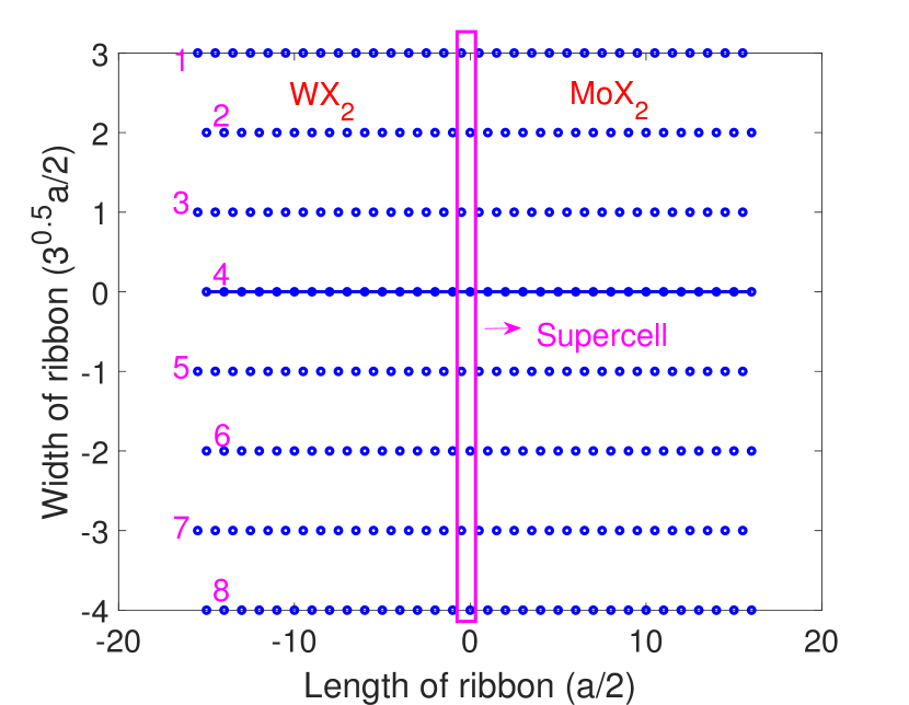
Now let us find the binding energy of exciton numerically. Fig.1 shows the triangular grid of a lateral heterostructure of 2D-TMDs with an armchair interface. If the scale of -axis is multiplied by (), the structure of the zigzag interface will be found.
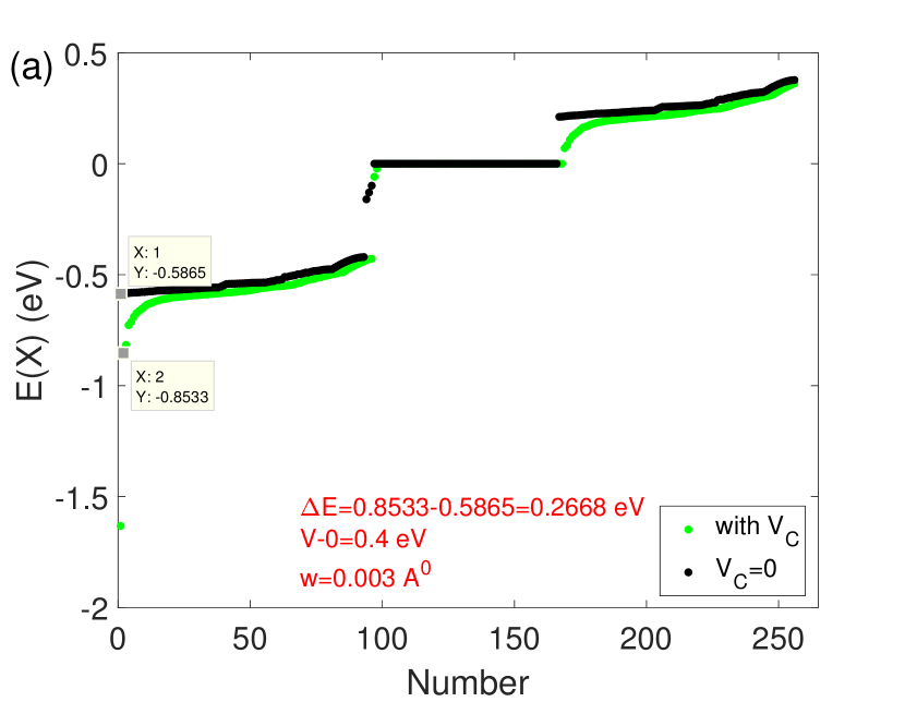
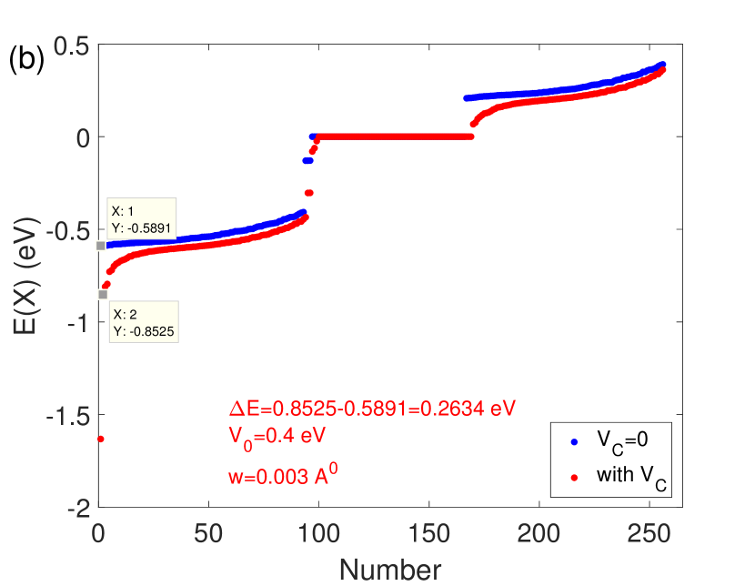
First, we consider the armchair interface. Here, the hopping integral is equal to 0.0218 eV because and Angstrom () Lau et al. (2018). In the type-II heterostructures, the interface is atomically sharp, and in consequence, we can set in Eq.21. Because, for the value of from Eq.20 will be at the order of , we set eV and will show how its effects on the final results can be compensated by a suitable choice of band offset energy, . Fig.2 shows a typical comparison between and . It should be noted that in each supercell, there are eight atoms, and four of them have the same x-coordinate, and consequently, the same lattice potential .
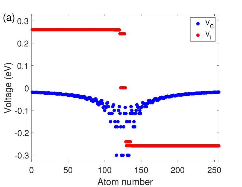
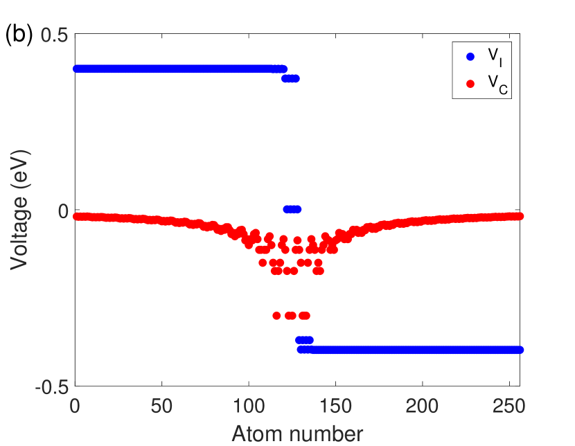
(not shown). eV. eV.
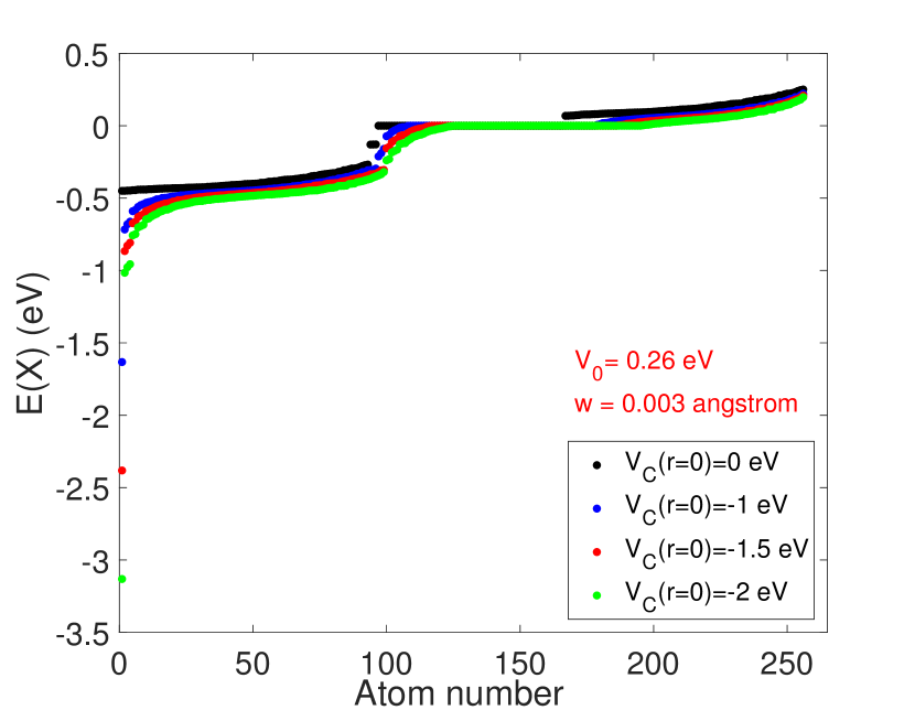
As Fig.2 shows the Coulomb potential has a significant value only at the interface and couples the electrons and holes at the region. For studying the effect of , we should obtain for different values of by attention to the value of the band offset voltage. It has been shown that there are two characteristic behaviors, the regime of small band offset ( eV) and large band offset ( eV) Lau et al. (2018). For sufficiently large , the electron and hole are well separated into opposite regions, while for small and intermediate , the separation is weak, and in consequence, on-site Coulomb interaction plays the main role. For example, it has been shown that for eV, the binding energy of the interface exciton is about 0.22 eV which is about 0.1 eV smaller than that of the 2D exciton Lau et al. (2018). The effect of Coulomb potential on the energy of excitons () is shown in Fig.3, for eV. It can be seen that the exciton energy depends on because at some atomic sites near the interface (Fig.2(a)). However, for eV, as Fig.4 shows, the second minimum eigenvalue does not change when the value of changes. Under this condition, and lattice potential dominates (Fig.2(b)), and therefore, the effect of on the second minimum of eigenvalue is negligible. We consider eV and the second minimum eigenvalue as in the next calculations and will show that under these conditions the correct binding energy can be calculated for MoX2-WX2 LHSs. Also, as Fig.4 shows, the Coulomb potential decreases the second minimum of energy by 0.26 eV. It means that the system is more stable now. As the first approximation, we can consider the difference as the binding energy of exciton which is of the same order as a two-dimensional exciton in TMDs. In what follows, we will show that under which conditions the approximation is satisfied.
eV.
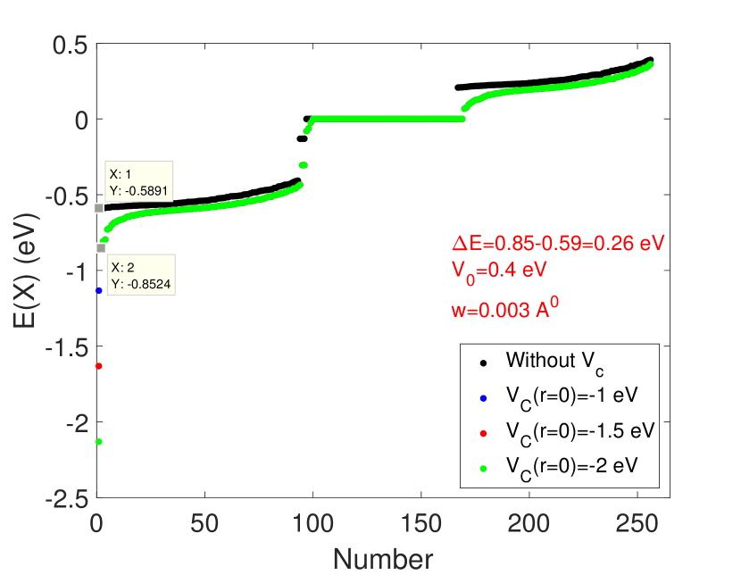
eV.
Our guess for the wave function of center-of-mass was where . As electron and hole are well separated into opposite regions for eV even for very long nanoribbon Lin, Williams, and Connell (2010); Liu et al. (2015) and considering the behavior and value of the Coulomb potential compared to the lattice potential (Fig.2(b)), it is expected that decays to of its maximum value for a specific value of (called . For we have and in consequence:
| (23) |
Therefore, by increasing (well separation of electron and hole) the term decreases rapidly and . But, the minimum value of is equal to Angstrom when one electron is at interface () and one hole is at (). So, the maximum value of eV and . Under this condition, eV which is equal to the binding energy of 2D exciton, approximately Lau et al. (2018). As a result, it can be concluded that near the interface eV and far from it eV. It means that the binding energy of exciton depends on its distance from the interface.
Now let us, study the effect of the interface structure on binding energy. Fig. 5 shows the comparison between the binding energy of zigzag and armchair interfaces. As it shows, the difference is meV. is created by the deformation gauge field which is a pseudo spin-orbit coupling. Its value is small due to its nature.
eV.
V Summary
We studied the dark exciton in two –dimensional dichalcogenide LHSs with a sharp interface. We introduced a low-energy effective Hamiltonian model and found the energy dispersion relation of exciton and showed how it depends on the onsite energy of composed materials and their spin-orbit coupling strengths. It was shown that the balance between the Coulomb and offset potential implies the behavior of exciton, especially at the interface. Also, by assigning a deformation gauge field to the geometrical structure of the interface, we could find the effect of the geometry on the binding energy of exciton. By discretization of the real-space version of dispersion relation on a triangular lattice, the exciton binding energy calculated as 0.34 eV near (far from) the interface i.e., the binding energy of exciton depends on its distance from the interface line. Finally, we could show that the binding energy of a zigzag interface increases by 0.34 meV in comparison with an armchair interface due to the pseudo-spin-orbit coupling term (deformation gauge field). The results can be useful in the design of new optoelectronic devices with improved performance and characteristics.
VI Data availablity
The data that supports the findings of this study are available within the article and its Appendices.
Appendix A
The low-energy two-band effective Hamiltonian of spin-up electrons near the K-point is given by Xiao et al. (2012)
| (24) |
where, , and , , and are the energy band gap, lattice constant, and hopping integral, respectively. Here, is the spin-orbit coupling (SOC) strength. It can be shown that the eigenvalues are given by
| (25) |
By defining = and , one can easily diagonalize the Hamiltonian, , by using the matrix and shows
| (26) |
For , the energy eigenvalues are and in consequence the conduction band minimum (CBM) and valence band maximum (VBM) are equal to and , respectively. For spin-down electrons, CBM and VBM are and , respectively. So, the band splitting happens at VBM by the SOC.
If the eigenfunctions and are used it can be shown that
| (27) |
| (28) |
For adding a gauge field, , to the Hamiltonian, we should use the covariant derivatives. It means that we should replace by in the Hamiltonian matrix. If we consider the equation , it can be shown that
| (29) |
where, is Fermi velocity, , , and . If , and by neglecting the term , it can be shown that
| (30) |
If then
| (31) |
and
| (32) |
Therefore, the term is pseudo-spin orbit coupling and splits not only VBM but also CBM. Because for the Eq.(A-6) has a non-trivial solution, the surface states exist.
Appendix B
In -plane, one can define three vectors , , and and shows that
| (33) |
| (34) |
| (35) |
In a triangular lattice, and and in consequence Evans (2007)
| (36) |
Now by discretizing the right-hand side of the Eq.(B-4), the below equation can be derivedEvans (2007)
| (37) |
where, , , and are in , , and directions. Therefore, the hopping integral is equal to where, is the lattice constant.
Appendix C
It is assumed that two electric charges and are located at positions and , respectively in a slab of dielectric constant . The slab width is and is surrounded by a medium of dielectric constant and a medium of dielectric constant . Felbacq et al., have shown that the electrostatic energy between both charges is given byFelbacq and Rousseau (2019):
| (38) |
where, is the dielectric constant of slab, , , , and . Here,
| (39) |
where and is Bessel function. By proofing a theorm, they have shown that the kernel of the first integral tends exponentially fast toward zero and it defines a function that regular near the origin . It means that the screened electrostatic potential in a dielectric slab can be considered as the usual Coulomb potential plus a correction termFelbacq and Rousseau (2019). If the slab width is large compared to the relative distance between the two electric charges the correction term is exponentially small. Also, if the height z approaches zero, the expression does not present any divergenceFelbacq and Rousseau (2019). The expression is suitable for further numerical calculations aiming to compute the binding energy of excitons in quasi-2D materialsFelbacq and Rousseau (2019).
References
- Lin, Williams, and Connell (2010) Y. Lin, T. Williams, and J. Connell, Phys. Chem. Lett. 1, 277 (2010).
- Weng et al. (2016) Q. Weng, X. Wang, X. Wang, Y. Bando, and D. Golberg, Chem. Soc. Rev. 45, 3989 (2016).
- Lv et al. (2015) R. Lv, J. Robinson, R. Schaak, D. Sun, Y. Sun, T. Mallouk, and M. Terrones, Acc. Chem. Res. 48, 56 (2015).
- Tan and Zhang (2015) C. Tan and H. Zhang, Chem. Soc. Rev. 44, 2713 (2015).
- Liu et al. (2015) H. Liu, Y. Du, Y. Deng, and P. Ye, Chem. Soc. Rev. 44, 2732 (2015).
- Chen et al. (2018) P. Chen, N. Li, X. Chen, W. Ong, and X. Zhao, 2D Mater. 5, 014002 (2018).
- Kara et al. (2012) A. Kara, H. Enriquez, A. Seitsonen, L. Voon, S. Vizzini, B. Aufray, and H. Oughaddou, Surf. Sci. Rep. 67, 1 (2012).
- Duan et al. (2014a) X. Duan, C. Wang, J. C. Shaw, R. Cheng, Y. Chen, H. Li, X. Wu, Y. Tang, Q. Zhang, A. Pan, J. Jiang, R. Yu, Y. Huang, and X. Duan, Nanotechnol. 9, 1024 (2014a).
- Heo et al. (2015) H. Heo, J. H. Sung, G. Jin, J. H. Ahn, K. Kim, M. J. Lee, S. Cha, H. Choi, and M. H. Jo, Adv. Mater. 27, 3803 (2015).
- Gong et al. (2015) Y. Gong, S. Lei, G. Ye, B. Li, Y. He, K. Keyshar, X. Zhang, Q. Wang, J. Lou, Z. Liu, R. Vajtai, W. Zhou, and P. M. Ajayan, Nano Lett. 15, 6135 (2015).
- Zhang et al. (2017) Z. Zhang, P. Chen, X. Duan, K. Zang, J. Luo, and X. Duan, Science 357, 788 (2017).
- Huang et al. (2014) C. Huang, S. Wu, A. M. Sanchez, J. J. P. Peters, R. Beanland, J. S. Ross, P. Rivera, W. Yao, D. H. Cobden, and X. Xu, Nat. Mater. 13, 1096 (2014).
- Gong et al. (2014) Y. Gong, J. Lin, X. Wang, G. Shi, S. Lei, Z. Lin, X. Zou, G.Ye, R. Vajtai, B. I. Yakobsoni, H. Terrones, M. Terrones, B. K. Tay, J. Lou, S. T. Pantelides, Z. Liu, W. Zhou, and P. Ajayan, Nat. Mater. 13, 1135 (2014).
- Zhang et al. (2015a) X. Q. Zhang, C. H. Lin, Y. W. Tseng, K. H. Huang, and Y. H. Lee, Nano Letters 15, 410 (2015a).
- Mahjouri-Samani et al. (2015) M. Mahjouri-Samani, M. W. Lin, K. Wang, A. R. Lupini, J. Lee, L. Basile, A. Boulesbaa, C. M. Rouleau, A. A. Puretzky, I. N. Ivanov, K. Xiao, M. Yoon, and D. B. Geohegan, Nat. Commun. 6, 7749 (2015).
- Gong et al. (2013) C. Gong, H. Zhang, W. Wang, L. Colombo, R. M. Wallace, and K. Cho, Appl. Phys. Lett. 103, 053513 (2013).
- Kosmider and Rossier (2017) K. Kosmider and J. F. Rossier, Phys Rev B 87, 075451 (2017).
- Kang et al. (2013) J. Kang, S. Tongay, J. Zhou, J. Li, and J. Wu, Appl. Phys. Lett. 102, 012111 (2013).
- Ozcelik et al. (2016) V. O. Ozcelik, J. G. Azadani, C. Yang, S. J. Koester, and T. Low, Phys. Rev. B 94, 035125 (2016).
- Zhang et al. (2016) Z. Zhang, Y. Xie, Q. Peng, and Y. Chen, Sci. Rep. 6, 21639 (2016).
- Avalos-Ovando, Mastrogiuseppe, and Ulloa (2019) O. Avalos-Ovando, D. Mastrogiuseppe, and S. E. Ulloa, Phys. Rev. B 99, 035107 (2019).
- Choukroun et al. (2019) J. Choukroun, M. Pala, S. Fang, E. Kaxiras, and P. Dollfus, Nanotechnology 30, 025201 (2019).
- Duan et al. (2014b) X. Duan, C. Wang, J. Shaw, R. Cheng, and Y. C. et al., (2014b), Nat. Nanotechnol. .
- Li et al. (2018) M. Li, J. Pu, J. Huang, Y. Miyauchi, K. Matsuda, T. Takenobu, and L. Li, Adv. Funct. Mater. 28, 1706860 (2018).
- Chen et al. (2019) D. Chen, M. Hofmann, H. Yao, S. Chiu, S. Chen, Y. Luo, C. Hsu, and Y. Hsieh, ACS Appl. Mater. Interfaces 11, 6384 (2019).
- Amani et al. (2015) M. Amani, D. H. Lien, D. Kiriya, J. Xiao, A. Azcatl, J. Noh, S. R. Madhvapathy, R. Addou, K. Santosh, and M. Dubey, Science 4, 350 (2015).
- Godde et al. (2016) T. Godde, D. Schmidt, J. Schmutzler, M. Asmann, J. Debus, F. Withers, E. M. Alexeev, O. D. Pozo-Zamudio, O. V. Skrypka, K. S. Novoselov, M. Bayer, and A. I. Tartakovskii, Phys. Rev. B 94, 165301 (2016).
- Zhang et al. (2015b) X. Zhang, Y. You, S. Y. F. Zhao, and T. F. Heinz, Phys. Rev. Lett. 115, 257403 (2015b).
- Rivera, Yao, and et al. (2015) P. Rivera, W. Yao, and X. D. X. et al., ., Nat. Commun. 6, 6242 (2015).
- Li et al. (2015) Y. M. Li, J. Li, L. K. Shi, D. Zhang, W. Yang, and K. Chang, Phys. Rev. Lett. 115, 166804 (2015).
- Latini, Olsen, and Thygesen (2015) S. Latini, T. Olsen, and K. S. Thygesen, Phys. Rev. B 92, 245123 (2015).
- Lau et al. (2018) K. W. Lau, Calvin, Z. Gong, H. Yu, and W. Yao, Phys. Rev. B 98, 115427 (2018).
- Jin et al. (2019) H. Jin, V. Michaud, Z. R. Gong, L. Wan, Y. Wei, and H. Guo, J. Mater. Chemi. 7, 13 (2019).
- Sasaki, Murakami, and Saito (2006) K. Sasaki, S. Murakami, and R. Saito, J. Phys. Soc. Jpn 75, 7 (2006).
- Liu et al. (2014) G. B. Liu, W. Y. Shan, Y. Yao, W. Yao, and D. Xiao, Phys. Rev. B 89, 039901 (2014).
- Cudazzo, Tokatly, and Rubio (2011) P. Cudazzo, I. V. Tokatly, and A. Rubio, Phys. Rev. B 84, 085406 (2011).
- Hai (2011) D. S. Hai, Commum. Theor. Phys. 55, 969 (2011).
- Sous and Alhaidari (2016) A. J. Sous and A. D. Alhaidari, J. Appl. Mathe. and Phys. 4, 79 (2016).
- Gonzalez-Espimoza and Ayers (2016) C. E. Gonzalez-Espimoza and P. W. Ayers, Theor. Chemist. Accou. 135, 256 (2016).
- Sous and EI-Kawni (2018) A. J. Sous and M. I. EI-Kawni, J. Appl. Mathe. and Phys. 6, 901 (2018).
- Chaves and Jimenez (2018) F. A. Chaves and D. Jimenez, Nanotech. 29, 27 (2018).
- Felbacq and Rousseau (2019) D. Felbacq and E. Rousseau, Ann. Phys. (Berlin) 531, 1800486 (2019).
- Zhang and Ma (2019) J. Z. Zhang and J. Z. Ma, Conden. Matt. 31, 10 (2019).
- Pulci et al. (2015) O. Pulci, M. Marsili, V. Garbuio, P. Gori, I. Kupchak, and F. Bechstedt, Phys. Stat. Sol. B 252, 72 (2015).
- Xiao et al. (2012) D. Xiao, G. B. Liu, W. Feng, X. Xu, and W. Yao, Phys. Rev. Lett. 108, 196802 (2012).
- Evans (2007) D. J. Evans, Int. J. Comput. Math. 39, 1 (2007).