Electronic, thermal, and optical properties of graphene like SiCx structures:
Significant effects of Si atom configurations
Abstract
We investigate the electronic, thermal, and optical characteristics of graphene like SiCx structure using model calculations based on density functional theory. The change in the energy bandgap can be tuned by the Si atomic configuration, rather than the dopants ratio. The effects of the concentration of the Si atoms and the shape of supercell are kept constant, and only the interaction effects of two Si atoms are studied by varying their positions. If the Si atoms are at the same sublattice positions, a maximum bandgap is obtained leading to an increased Seebeck coefficient and figure of merit. A deviation in the Wiedemann-Franz ratio is also found, and a maximum value of the Lorenz number is thus discovered. Furthermore, a significant red shift of the first peak of the imaginary part of the dielectric function towards the visible range of the electromagnetic radiation is observed. On the other hand, if the Si atoms are located at different sublattice positions, a small bandgap is seen because the symmetry of sublattice remains almost unchanged. Consequently, the Seebeck coefficient and the dielectric function are only slightly changed compared to pristine graphene. In addition, the electron energy loss function is suppressed in Si-doped graphene. These unique variations of the thermal and the optical properties of Si-doped graphene are of importance to understand experiments relevant to optoelectronic applications.
keywords:
Energy harvesting , Thermal transport , Optical properties , Graphene , Density Functional Theory , Electronic structure1 Introduction
The discovery of carbon-related materials and their development has been considered to be crucial for the future of technology [1, 2, 3, 4, 5, 6]. Carbon based material such as monolayer graphene offers good possibility of device performance down to the atomic limit [7]. Extraordinary properties of graphene make it an interesting material for many electronic devices. The zero band gap of graphene leads it to be a metallic like material with nontrivial physical properties such as high electron mobility at room temperature and exceptional thermal conductivity [8]. The bandgap of graphene can be tuned by several techniques termed functionalization strategies [9], doping [10], application of an electric field [11] or a magnetic field [12], or strain [13], etc. Among these methods, the doping process is considered one of the most feasible ways to tune the bandgap of graphene and altering its physical characteristics, for the reason that doping can break or alter the symmetric structure of graphene [14].
The integration of two-dimensional graphene into silicon chips promises a better heterogeneous platform to deliver a massively enhanced potential based on silicon technology [15]. Silicon doped graphene systems (SixCy) have emerged as new 2D materials called siligraphenes. They have been considered as good composite materials based on graphene to study enormously interesting physical application such as solar cell devices [16] and gas sensors [17]. Si-substituted graphenes have been identified as significant structures for technological application [18]. The ratio of the Si doping in graphene determines the potential or the functionality of the structure. For instance, SiC2 can be used to built solar cell devices due to its finite band gap [16], SiC3 and SiC5 can be used as topological insulators and semi-metals [17, 19], while SiC7 is suggested for photovoltaic devices [20, 21].
In recent years, the investigation of thermal properties of graphene like SiCx structures (g-SiCx) has been attracting the attention of many researchers, and the interest in the subject is still growing [22, 23]. It has been shown that the electrical and thermal properties of two configurations of siligraphene, g-SiC3 and g-SiC7 can be tuned by the concentration of the silicon. The thermal conductivity of g-SiC7 is exponentially enhanced with temperature, but it varies parabolically for g-SiC3 [24, 25]. Composite thermal interface materials have been optimized with an admixture of graphene structures with different doped materials leading to a high enhancement of the effective thermal conductivity [5], which has been beneficial for large range of materials used by industry. Therefore, graphene based materials can be used for energy harvesting and increased efficiency of solar cell devices at room temperature due to a high-recorded thermal property dominated by the acoustic phonons [26].
Optical properties of g-SiCx is another important aspect of research in which the g-SiCx has been used for solar cell application. Optical properties such as the optical conductivity, reflectivity and refractive index have been studied and it has been demonstrated that the optical conductivity is enhanced due to the Si-dopant [27, 28]. Theoretical studies have shown that the bandgap of g-SiCx is decreased with increasing applied external electrical field intensity. The dielectric functions and the refractive indexes at low frequency are decreased compared with those of pristine graphene [29]. Furthermore, the optical absorption spectra of a Si-doped graphene are dominated by bound Frenkel exciton and the Si-dopant enhances the optical conductivity of graphene in the visible range [30].
In this work, we model Si-doped graphene nanosheets with a concentration ratio of Si-atoms. We will show the influence of Si atomic configurations, and the Si-Si interactions on the electronic, thermal and optical characteristics using model calculations based on Density Functional Theory (DFT) [31, 32, 33].
2 Computational Tools
We consider two-dimensional Si-doped sheet of graphene with atoms consisting of carbon and silicon atoms. It is configured into a supercell with Si doping concentration ratio. The electronic properties of the systems are calculated within a self-consistent field (SCF) approximation. We use a Kohn-Sham local density approximation [34] augmented a with generalized gradient approximation (GGA), as implemented by the Quantum Espresso (QE) package for the band structure and the density of states of the systems [35].
The Brillouin zone is sampled using a -centered -point grid and atomic relaxations are continued until the Helmann-Feynman forces acting on the atoms is less than and the total energy changes are less than eV. In addition, the convergence criteria of the SCF and the non-SCF of density of state calculations are set to be eV with an , and a -point grid, respectively. A plane-wave projector-augmented wave (PAW) method with a kinetic energy cut-off equal to eV is implemented in the DFT code [36, 37, 38, 39]. Furthermore, the exchange-correlation function calculated by the non-relativistic Perdew Burke Ernzerhof (PBE) approach is utilized in our model using the QE package [40].
The calculations of the thermal properties of the systems are carried out using the Boltzmann theory implemented in the BoltzTraP package [41, 42]. The BoltzTraP code uses a mesh of band energies and is well documented within the QE guidelines. We calculate the Seebeck coefficient, , the figure of merit, , of the systems. In the BoltzTraP, the Seebeck coefficient is given by [43]
| (1) |
where
| (2) |
Herein, is the unit charge, is the Boltzmann’s constant, indicates the number of -points, refers to the unit cell volume, is the electrical conductivity, is the band energy, represents Fermi-Dirac distribution function, stands for the chemical potential, is the temperature measured in Kelvin, is the relaxation time, is the group velocity of the charges, and is the Dirac delta function. The subscripts and mean the crystal momentum and the band index [41, 44].
In addition, the is defined by the following equation:
| (3) |
where is the sum of both the electron and the phonon thermal conductivity.
The imaginary part of dielectric function , in the long wavelength limit, can be obtained directly from the electronic structure calculation
| (4) |
where are the dipole transition matrix elements [45].
3 Results
In this section, we present the main results calculated via DFT. We consider three Si doped graphene structures in addition to pure graphene (PG) as shown in Fig. 1(a-d). The three Si-doped graphene structures are: First, the two Si atoms (yellow) are doped at a para- and an ortho-position which means that the Si atoms are adjacent. The structure is identified as a g-SiC-1 (b). So, the two Si atoms are at different sublattice positions in which one dopant atom is placed at sublattice A and the other is at B. Second, the two Si atoms are put at the para- and the meta-position, the Si atoms are at the same sublattice positions (either A or B), forming g-SiC-2 (c).
Finally, the two Si atoms are both located at a para-position, resulting in g-SiC-3, shown in (d), in this case the two Si atoms are at different lattice positions [46, 47].
Among these Si-doped structures, g-SiC-1 seems to be less structurally stable compared to g-SiC-2 and g-SiC-3 since sp2-hybridization is not favored by Si–Si bonds, a planar structure should be energetically unfavorable [48].
The electron charge distributions of the four structures are plotted in Fig. 1 (contour plots). The high electron charge distribution between the carbon atoms in the PG indicates strong and stiff covalent bonds forming between the C atoms. Therefore, PG boasts of great stability and a very high tensile strength (the force with which one can stretch something before it breaks) [49]. In the g-SiC-1 structure, the Si atoms form Si-Si bonds and the electron charge distribution between the Si atoms is very weak because of the presence a strong repulsive force between the Si atoms. Furthermore, the C-Si bonds are somewhat polarized towards the C atoms due to carbon’s greater electronegativity. The electron charge distribution thus concentrates around the C atoms.
The same scenarios for electron charge distribution are also true for the other two Si-doped structures, g-SiC-2 and g-SiC-3. The electron charge distributions of all three Si-doped structures confirm that the C-Si bonds are longer and weaker than the C–C bonds. This could be expected because of the larger atomic radius of a Si compared to a C atom.
Electronic band structure is calculated along the high-symmetry -K-M- directions. By looking at the band structures, we can see that the conduction and valence bands touch at the Fermi level, zero energy, as is presented in Fig. 1(e) for PG. One can see from the band structures in Fig. 1(f–h) that the maximum band gap appears for g-SiC-2 and it is equal to meV. The category of g-SiC-2 originates when both the Si dopants are placed at the same sublattice positions (either A or B). This observation confirms that the origin of the bandgap is due to symmetry breaking of graphene sublattices, which is maximized in these configurations. The same scenario has been seen for Boron or Nitrogen doped graphene [46].
3.1 Thermal properties
We display thermoelectric properties at K which is in the intermediate temperature range, K, where the electron and the lattice temperatures are decoupled. The electronic thermal conductivity is thus proportional to the charge conductivity at a given temperature. In this temperature range, the electron and the lattice temperatures are very well decoupled in low-disorder graphene [50, 51].
Figure 2 shows the contributions of the electrons to different thermoelectric parameters, the Seebeck coefficient (a) and the figure of merit (b). In general, semiconductor materials with high a bandgap effectively minimize free charge carrier contributions. The Seebeck coefficient is thus enhanced since is inversely proportional to charge carrier concentration [52]. The Seebeck coefficient is found to be significant and as high as mV K-1 for g-SiC-2 (green line), higher than the value of 6 V K-1 for PG. The enhancement of the Seebeck coefficient is attributed to the existence of the high bandgap of g-SiC-2 compared to PG. In addition, the Seebeck coefficient of g-SiC-1 and g-SiC-3 is smaller than that of g-SiC-2 due to the smaller bandgaps of these two structures.
Figure of merit is what ultimately would determine the efficiency of the devices. It is interesting to compare the of the four aforementioned structures. One can see that increased Seebeck coefficient raises the enhancement of figure of merit as is presented in Fig. 2(b), where the maximum is found for g-SiC-2 (green line).
We now consider the Wiedemann-Franz (WF) law for our model. The WF law states that the ratio of to is given by
| (5) |
which is constant for ordinary metals, where W K-2, called the Lorenz number [53, 54]. For graphene, the low chemical potential makes the Lorenz number sensitive to resonance scattering and the energy dependence of the relaxation time [55]. Figure 3 displays the Lorenz factor for all four structures shown in Fig. 1 at the intermediate temperature K. It can clearly be seen that strongly depends on the energy or chemical potential, especially around the resonance states. In addition, the value of depends on the location of the resonance states of the different Si atomic configuration in our calculations. The maximum value of W K-2 is found for g-SiC-2. We conclude that the WF law is not obeyed in our Si-doped graphene structures at K [50].
3.2 Optical properties
Graphene has unique optical characteristics and can absorb a wide range of electromagnetic radiation [56]. PG is known to emit light when it has been excited by a near-infrared laser [57]. In the case of doped graphene, photoluminescence is observed by creation of a bandgap [58].
We use the three aforementioned silicon atom configurations to investigate the optical properties of doped graphene. The imaginary part of the dielectric function, , is presented in Fig. 4 for PG (brown), g-SiC-1 (blue), g-SiC-2 (green), and g-SiC-3 (red) in the case of parallel (a) and perpendicular (b) electric field. In the case of PG, two peaks in the imaginary part of dielectric function for a parallel electric field are observed (brown line), one at eV indicating transition and another at eV displaying transition. The position of both peaks in our calculation is in a good agreement with the literature [59, 60]. The intensity ratio of these two peaks is demonstrating that the transition is stronger than the transition. This is what should be obtained for monolayer pure graphene. In the case of a perpendicular electric filed Fig. 4(b), two main peaks for PG appear at and eV belonging to the and the transitions, respectively.
Let’s look at the effect of silicon doping of graphene on the imaginary part of dielectric function. It is interesting to see an extra peak at eV, in the visible range, in the case of a parallel electric field for g-SiC-2 (see the inset of Fig. 4(a)) [61]. The extra peak can be referred to the existence of a finite bandgap. Our analysis shows a significant red shift of the first peak of the dielectric function towards the visible range. The peak structure becomes more complex due to the Si doping, and more peaks may be identified in the visible range. Furthermore, the intensity of both peaks is decreased in the case of Si-doping for perpendicular electric field as is shown in Fig. 4(b). This indicates that both transitions, and , are weaker compared to the corresponding transitions active in PG. These unique variations of the dielectric function of Si doped graphene are of importance to understand relevant experiments and design for optoelectronic applications [62, 63].
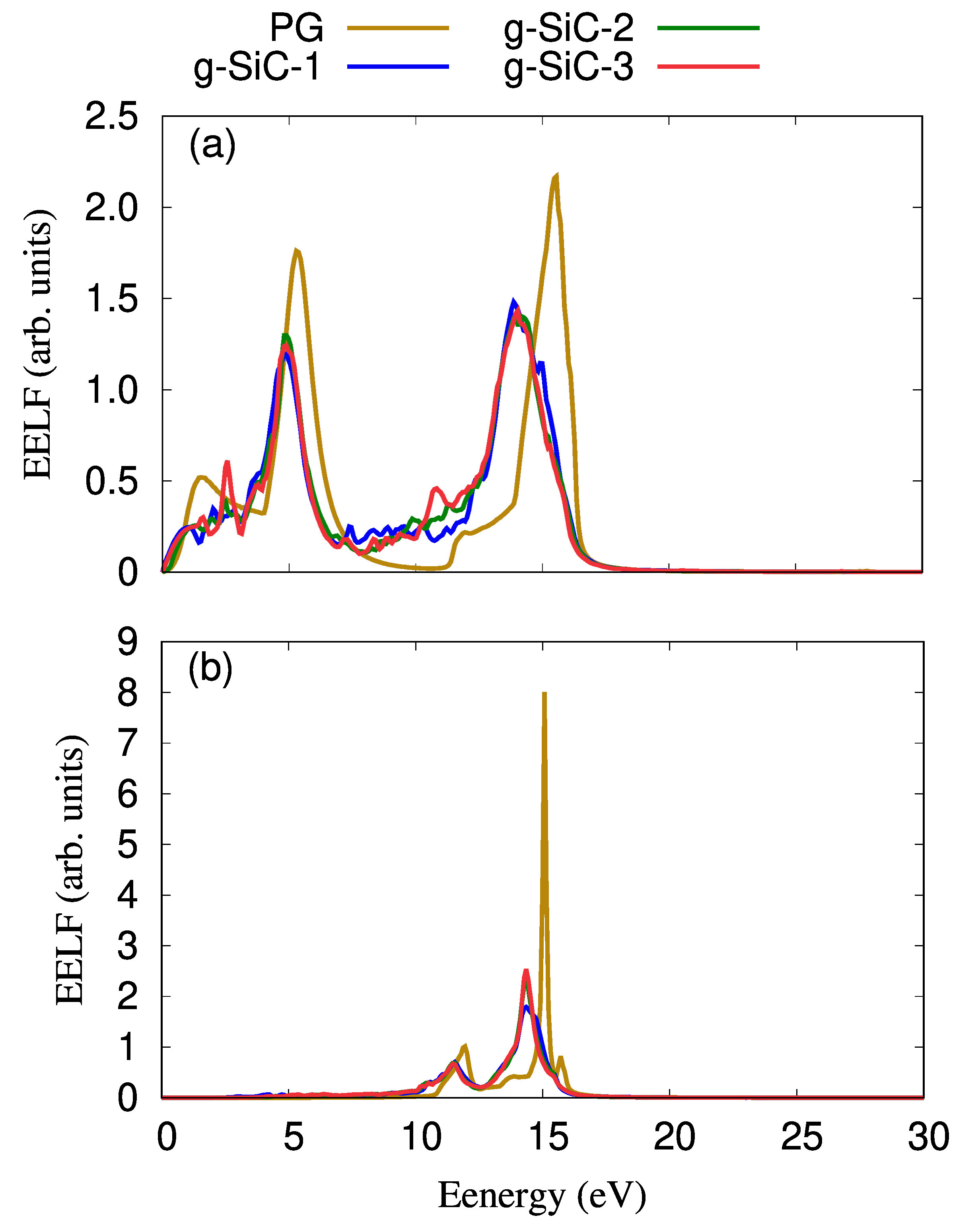
The electron energy-loss function (EELF) is shown in Fig. 5 in the presence of parallel (a) and perpendicular (b) electric field for PG (brown), g-SiC-1 (blue), g-SiC-2 (green), and g-SiC-3 (red). The electron inelastic interaction with a structure is closely related to the EELF which represents the probability of inelastic scattering events. It can clearly be seen that the EELF is decreased for all three Si-doped graphene structures. This is attributed to the low probability of charge concentration close to a Si-dopant in the graphene nanosheets [60]. It should be mentioned that EELS obtains a maximum value where has a finite small value. So, plasmonic excitations can be responsible for the maximum intensity of EELS peak [64].
4 Conclusion
In summary, the characteristics of monolayer graphene-like materials with SiCx stoichiometry are investigated where the position of the Si atoms plays an important role for their physical properties. The electronic band structure of graphene can be remarkably modulated by different Si doping configurations, leading to Dirac point shifting and even opening of bandgaps. Consequently the figure of merit is enhanced. In addition, the optical properties, such as the dielectric and the electron energy loss function are influenced by the tuning of the bandgap. As a result, a reduction in electron energy loss function has been found, and an extra peak in imaginary part of the dielectric function towards the visible range is found. Last but not least, we show that our model does not obey the Wiedemann-Franz law. Therefore, a maximum value of Lorenz number is found around resonant scattering states.
5 Acknowledgment
This work was financially supported by the University of Sulaimani and the Research center of Komar University of Science and Technology. The computations were performed on resources provided by the Division of Computational Nanoscience at the University of Sulaimani.
References
- [1] Deji Akinwande, Cedric Huyghebaert, Ching-Hua Wang, Martha I. Serna, Stijn Goossens, Lain-Jong Li, H. S Philip Wong, and Frank H. L. Koppens. Graphene and two-dimensional materials for silicon technology. Nature, 573(7775):507–518, 2019.
- [2] Phaedon Avouris. Graphene: Electronic and photonic properties and devices. Nano Letters, 10(11):4285–4294, 2010. PMID: 20879723.
- [3] Amin Salehi-Khojin, David Estrada, Kevin Y. Lin, Ke Ran, Richard T. Haasch, Jian-Min Zuo, Eric Pop, and Richard I. Masel. Chemical sensors based on randomly stacked graphene flakes. Applied Physics Letters, 100(3):033111, 2012.
- [4] Changgu Lee, Xiaoding Wei, Jeffrey W. Kysar, and James Hone. Measurement of the elastic properties and intrinsic strength of monolayer graphene. Science, 321(5887):385–388, 2008.
- [5] Khan M. F. Shahil and Alexander A. Balandin. Thermal properties of graphene and multilayer graphene: Applications in thermal interface materials. Solid State Communications, 152(15):1331–1340, 2012.
- [6] Yuanbo Zhang, Yan-Wen Tan, Horst L. Stormer, and Philip Kim. Experimental observation of the quantum hall effect and berry’s phase in graphene. Nature, 438(7065):201–204, 2005.
- [7] René H. J. Vervuurt, Wilhelmus M. M. (Erwin) Kessels, and Ageeth A. Bol. Atomic layer deposition for graphene device integration. Advanced Materials Interfaces, 4(18):1700232, 2017.
- [8] Wei Yu, Huaqing Xie, Luqiao Yin, Junchang Zhao, Ligang Xia, and Lifei Chen. Exceptionally high thermal conductivity of thermal grease: Synergistic effects of graphene and alumina. International Journal of Thermal Sciences, 91:76–82, 2015.
- [9] Ankita Sinha, Dhanjai, Jiping Chen, and Rajeev Jain. Graphene Functionalization Strategies: From Synthesis to Applications, chapter Functionalized Graphene-Metal Nanoparticles Nanohybrids as Electrochemical Sensors, pages 49–62. Springer Singapore, Singapore, 2019.
- [10] Seon-Myeong Choi, Seung-Hoon Jhi, and Young-Woo Son. Controlling energy gap of bilayer graphene by strain. Nano Letters, 10(9):3486–3489, Sep 2010.
- [11] A. A. Avetisyan, B. Partoens, and F. M. Peeters. Electric-field control of the band gap and fermi energy in graphene multilayers by top and back gates. Phys. Rev. B, 80:195401, Nov 2009.
- [12] S. Bala Kumar, M. B. A. Jalil, S. G. Tan, and Gengchiau Liang. Magnetoresistive effect in graphene nanoribbon due to magnetic field induced band gap modulation. Journal of Applied Physics, 108(3):033709, 2010.
- [13] U. Monteverde, J. Pal, M.A. Migliorato, M. Missous, U. Bangert, R. Zan, R. Kashtiban, and D. Powell. Under pressure: Control of strain, phonons and bandgap opening in rippled graphene. Carbon, 91:266–274, 2015.
- [14] Hongtao Liu, Yunqi Liu, and Daoben Zhu. Chemical doping of graphene. J. Mater. Chem., 21:3335–3345, 2011.
- [15] Kinam Kim, Jae-Young Choi, Taek Kim, Seong-Ho Cho, and Hyun-Jong Chung. A role for graphene in silicon-based semiconductor devices. Nature, 479(7373):338–344, 2011.
- [16] Liu-Jiang Zhou, Yong-Fan Zhang, and Li-Ming Wu. Sic2 siligraphene and nanotubes: Novel donor materials in excitonic solar cells. Nano Letters, 13(11):5431–5436, 2013. PMID: 24134541.
- [17] Huilong Dong, Lu Wang, Liujiang Zhou, Tingjun Hou, and Youyong Li. Theoretical investigations on novel sic5 siligraphene as gas sensor for air pollutants. Carbon, 113:114–121, 2017.
- [18] Ruitao Lv, Maria Cristina dos Santos, Claire Antonelli, Simin Feng, Kazunori Fujisawa, Ayse Berkdemir, Rodolfo Cruz-Silva, Ana Laura Elías, Nestor Perea-Lopez, Florentino López-Urías, Humberto Terrones, and Mauricio Terrones. Large-area si-doped graphene: Controllable synthesis and enhanced molecular sensing. Advanced Materials, 26(45):7593–7599, 2014.
- [19] Mingwen Zhao and Ruiqin Zhang. Two-dimensional topological insulators with binary honeycomb lattices: siligraphene and its analogs. Phys. Rev. B, 89:195427, May 2014.
- [20] Huilong Dong, Liujiang Zhou, Thomas Frauenheim, Tingjun Hou, Shuit-Tong Lee, and Youyong Li. Sic7 siligraphene: a novel donor material with extraordinary sunlight absorption. Nanoscale, 8(13):6994–6999, 2016.
- [21] Nzar Rauf Abdullah, Thorsten Arnold, Chi-Shung Tang, Andrei Manolescu, and Vidar Gudmundsson. Photon-induced tunability of the thermospin current in a rashba ring. Journal of Physics: Condensed Matter, 30(14):145303, mar 2018.
- [22] Byoung Seo Lee and Joon Sik Lee. Thermal conductivity reduction in graphene with silicon impurity. Applied Physics A, 121(3):1193–1202, Nov 2015.
- [23] Ishtiaque Ahmed Navid and Samia Subrina. Thermal transport characterization of carbon and silicon doped stanene nanoribbon: an equilibrium molecular dynamics study. RSC Adv., 8:31690–31699, 2018.
- [24] M. Houmad, A. El Kenz, and A. Benyoussef. Thermal and electrical properties of siligraphene and its derivatives. Optik, 157:936–943, 2018.
- [25] M. Houmad, I. Essaoudi, A. Ainane, A. El Kenz, A. Benyoussef, and R. Ahuja. Improving the electrical conductivity of siligraphene sic7 by strain. Optik, 177:118–122, 2019.
- [26] Alexander A. Balandin. Thermal properties of graphene and nanostructured carbon materials. Nature Materials, 10:569, Jul 2011. Review Article.
- [27] M. Houmad, H. Zaari, A. Benyoussef, A. El Kenz, and H. Ez-Zahraouy. Optical conductivity enhancement and band gap opening with silicon doped graphene. Carbon, 94:1021–1027, 2015.
- [28] Nzar Rauf Abdullah. Optical control of spin-dependent thermal transport in a quantum ring. Physics Letters A, 382(21):1432 – 1436, 2018.
- [29] Yuhua Wang, Weihua Wang, Shuyun Zhu, Ge Yang, Zhiqiang Zhang, and Ping Li. Theoretical studies on the structures and properties of doped graphenes with and without an external electrical field. RSC Adv., 9:11939–11950, 2019.
- [30] Masoud Shahrokhi and Céline Leonard. Tuning the band gap and optical spectra of silicon-doped graphene: Many-body effects and excitonic states. Journal of Alloys and Compounds, 693:1185–1196, 2017.
- [31] Hunar Omar Rashid, Nzar Rauf Abdullah, and Vidar Gudmundsson. Silicon on a graphene nanosheet with triangle- and dot-shape: Electronic structure, specific heat, and thermal conductivity from first-principle calculations. Results in Physics, 15:102625, 2019.
- [32] Nzar Rauf Abdullah, Hunar Omar Rashid, Mohammad T. Kareem, Chi-Shung Tang, Andrei Manolescu, and Vidar Gudmundsson. Effects of bonded and non-bonded b/n codoping of graphene on its stability, interaction energy, electronic structure, and power factor. Physics Letters A, 384(12):126350, 2020.
- [33] Nzar Rauf Abdullah, Hunar Omar Rashid, Chi-Shung Tang, Andrei Manolescu, and Vidar Gudmundsson. Modeling electronic, mechanical, optical and thermal properties of graphene-like bc6n materials: Role of prominent bn-bonds. arXiv:2003.08467 [cond-mat.mes-hall], 2020.
- [34] W. Kohn and L. J. Sham. Self-consistent equations including exchange and correlation effects. Phys. Rev., 140:A1133–A1138, Nov 1965.
- [35] Paolo Giannozzi, Stefano Baroni, Nicola Bonini, Matteo Calandra, Roberto Car, Carlo Cavazzoni, Davide Ceresoli, Guido L Chiarotti, Matteo Cococcioni, Ismaila Dabo, Andrea Dal Corso, Stefano de Gironcoli, Stefano Fabris, Guido Fratesi, Ralph Gebauer, Uwe Gerstmann, Christos Gougoussis, Anton Kokalj, Michele Lazzeri, Layla Martin-Samos, Nicola Marzari, Francesco Mauri, Riccardo Mazzarello, Stefano Paolini, Alfredo Pasquarello, Lorenzo Paulatto, Carlo Sbraccia, Sandro Scandolo, Gabriele Sclauzero, Ari P Seitsonen, Alexander Smogunov, Paolo Umari, and Renata M Wentzcovitch. QUANTUM ESPRESSO: a modular and open-source software project for quantum simulations of materials. Journal of Physics: Condensed Matter, 21(39):395502, sep 2009.
- [36] John P. Perdew, Kieron Burke, and Matthias Ernzerhof. Generalized gradient approximation made simple. Phys. Rev. Lett., 77:3865–3868, Oct 1996.
- [37] G. Kresse and D. Joubert. From ultrasoft pseudopotentials to the projector augmented-wave method. Phys. Rev. B, 59:1758–1775, Jan 1999.
- [38] P. E. Blöchl. Projector augmented-wave method. Phys. Rev. B, 50:17953–17979, Dec 1994.
- [39] Nzar Rauf Abdullah and Vidar Gudmundsson. Single-photon controlled thermospin transport in a resonant ring-cavity system. Physica E: Low-dimensional Systems and Nanostructures, 104:223 – 228, 2018.
- [40] Max Petersen, Frank Wagner, Lars Hufnagel, Matthias Scheffler, Peter Blaha, and Karlheinz Schwarz. Improving the efficiency of fp-lapw calculations. Computer Physics Communications, 126(3):294–309, 2000.
- [41] Georg K. H. Madsen and David J. Singh. Boltztrap. a code for calculating band-structure dependent quantities. Computer Physics Communications, 175(1):67–71, 2006.
- [42] Nzar Rauf Abdullah, Chi-Shung Tang, Andrei Manolescu, and Vidar Gudmundsson. Manifestation of the purcell effect in current transport through a dot–cavity–qed system. Nanomaterials, 9(7):1023, 2019.
- [43] M. W. Oh, D. M. Wee, S. D. Park, B. S. Kim, and H. W. Lee. Electronic structure and thermoelectric transport properties of agtlte: First-principles calculations. Phys. Rev. B, 77:165119, Apr 2008.
- [44] Nzar Rauf Abdullah, Chi-Shung Tang, Andrei Manolescu, and Vidar Gudmundsson. The photocurrent generated by photon replica states of an off-resonantly coupled dot-cavity system. Scientific Reports, 9(1):14703, 2019.
- [45] R. Khenata, A. Bouhemadou, M. Sahnoun, Ali. H. Reshak, H. Baltache, and M. Rabah. Elastic, electronic and optical properties of zns, znse and znte under pressure. Computational Materials Science, 38(1):29–38, 2006.
- [46] Pooja Rani and V. K. Jindal. Designing band gap of graphene by b and n dopant atoms. RSC Adv., 3:802–812, 2013.
- [47] Xiao-Lin Wei, Xun Wen, Li-Chun Xu, Xiang-Yang Peng, Li-Min Liu, Ru-Zhi Wang, and Jue-Xian Cao. Significant interplay effect of silicon dopants on electronic properties in graphene. Physics Letters A, 378(26):1841–1844, 2014.
- [48] Pengfei Li, Rulong Zhou, and Xiao Cheng Zeng. The search for the most stable structures of silicon-carbon monolayer compounds. Nanoscale, 6(20):11685–11691, 2014.
- [49] Hamzeh Kashani, Yoshikazu Ito, Jiuhui Han, Pan Liu, and Mingwei Chen. Extraordinary tensile strength and ductility of scalable nanoporous graphene. Science Advances, 5(2), 2019.
- [50] S. Yiğen and A. R. Champagne. Wiedemann–franz relation and thermal-transistor effect in suspended graphene. Nano Letters, 14(1):289–293, 2014. PMID: 24341325.
- [51] J. K. Viljas, A. Fay, M. Wiesner, and P. J. Hakonen. Self-heating and nonlinear current-voltage characteristics in bilayer graphene. Phys. Rev. B, 83:205421, May 2011.
- [52] Helin Zou, D.M Rowe, and Gao Min. Growth of p- and n-type bismuth telluride thin films by co-evaporation. Journal of Crystal Growth, 222(1):82–87, 2001.
- [53] Koichi Saito, Jun Nakamura, and Akiko Natori. Ballistic thermal conductance of a graphene sheet. Phys. Rev. B, 76:115409, Sep 2007.
- [54] S. G. Sharapov, V. P. Gusynin, and H. Beck. Transport properties in the d-density-wave state in an external magnetic field: The wiedemann-franz law. Phys. Rev. B, 67:144509, Apr 2003.
- [55] M. Inglot, A. Dyrdał, V. K. Dugaev, and J. Barnaś. Thermoelectric effect enhanced by resonant states in graphene. Phys. Rev. B, 91:115410, Mar 2015.
- [56] Yansong Fan, Chucai Guo, Zhihong Zhu, Wei Xu, Fan Wu, Xiaodong Yuan, and Shiqiao Qin. Monolayer-graphene-based broadband and wide-angle perfect absorption structures in the near infrared. Scientific Reports, 8(1):13709, 2018.
- [57] Peining Li, Tao Wang, Hannes Böckmann, and Thomas Taubner. Graphene-enhanced infrared near-field microscopy. Nano Letters, 14(8):4400–4405, 2014. PMID: 25019504.
- [58] Zhengtang Luo, Patrick M. Vora, Eugene J. Mele, A. T. Charlie Johnson, and James M. Kikkawa. Photoluminescence and band gap modulation in graphene oxide. Applied Physics Letters, 94(11):111909, 2009.
- [59] V. G. Kravets, A. N. Grigorenko, R. R. Nair, P. Blake, S. Anissimova, K. S. Novoselov, and A. K. Geim. Spectroscopic ellipsometry of graphene and an exciton-shifted van hove peak in absorption. Phys. Rev. B, 81:155413, Apr 2010.
- [60] T. Eberlein, U. Bangert, R. R. Nair, R. Jones, M. Gass, A. L. Bleloch, K. S. Novoselov, A. Geim, and P. R. Briddon. Plasmon spectroscopy of free-standing graphene films. Phys. Rev. B, 77:233406, Jun 2008.
- [61] Pooja Rani, Girija S. Dubey, and V.K. Jindal. Dft study of optical properties of pure and doped graphene. Physica E: Low-dimensional Systems and Nanostructures, 62:28–35, 2014.
- [62] Jingang Wang, Xijiao Mu, Mengtao Sun, and Tingjie Mu. Optoelectronic properties and applications of graphene-based hybrid nanomaterials and van der waals heterostructures. Applied Materials Today, 16:1 – 20, 2019.
- [63] Vidar Gudmundsson, Nzar Rauf Abdulla, Anna Sitek, Hsi-Sheng Goan, Chi-Shung Tang, and Andrei Manolescu. Electroluminescence caused by the transport of interacting electrons through parallel quantum dots in a photon cavity. Annalen der Physik, 530(2):1700334, 2018.
- [64] Namrata Dhar and Debnarayan Jana. Effect of beryllium doping and vacancy in band structure, magnetic and optical properties of free standing germanene. Current Applied Physics, 17(12):1589–1600, 2017.