Single-electron control in a foundry-fabricated two-dimensional qubit array
Silicon spin qubits have achieved high-fidelity one- and two-qubit gates Veldhorst2015 ; Muhonen2014 ; Watson2018 ; He2019 ; Zajac2018 , above error-correction thresholds Yoneda2018 , promising an industrial route to fault-tolerant quantum computation. A significant next step for the development of scalable multi-qubit processors is the operation of foundry-fabricated, extendable two-dimensional (2D) arrays. In gallium arsenide, 2D quantum-dot arrays recently allowed coherent spin operations and quantum simulations Mortemousque2018 ; Dehollain2019 . In silicon, 2D arrays have been limited to transport measurements in the many-electron regime Betz2016 . Here, we operate a foundry-fabricated silicon 2x2 array in the few-electron regime, achieving single-electron occupation in each of the four gate-defined quantum dots, as well as reconfigurable single, double, and triple dots with tunable tunnel couplings. Pulsed-gate and gate-reflectometry techniques permit single-electron manipulation and single-shot charge readout, while the two-dimensionality allows the spatial exchange of electron pairs. The compact form factor of such arrays, whose foundry fabrication can be extended to larger 2xN arrays, along with the recent demonstration of coherent spin control Maurand2016 and readout Crippa2019 ; Urdampilleta2019 , paves the way for dense qubit arrays for quantum computation and simulation Vandersypen2017 .
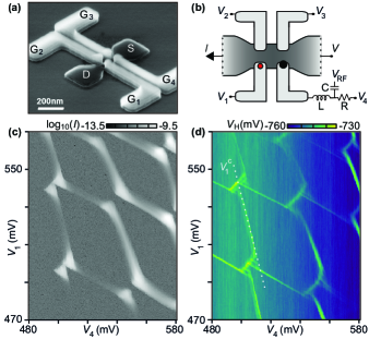
Our device architecture consists of an undoped silicon channel (Fig. 1a, dark grey) connected to a highly-doped source (S) and drain (D) reservoir. Metallic polysilicon gates (light grey) partially overlap the channel, each capable of inducing one quantum dot with a controllable number of electrons Barraud2016 ; Houtin2019 . While devices with a larger number of split-gate pairs are possible Chanrion2020 , we focus on a 22 quantum-dot array as the smallest two-dimensional unit cell in this architecture, i.e. a device with two pairs of split-gate electrodes, labelled Gn with corresponding control voltages . The device studied is similar to the one shown in Fig. 1a, but additionally has a common top gate 300 nm above the channel, and was encapsulated at the foundry by a back-end that includes routing to wirebonding pads. Quantum dots are induced in the 7-nm-thick channel by 32-nm-long gates, separated from each other by 32-nm silicon nitride (see Supplementary Information). The handle of the silicon-on-insulator wafer is grounded during measurements, but can in principle be utilized as a back gate.
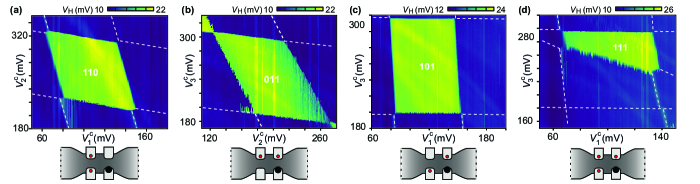
Figure 1b shows a schematic of the device with tuned to induce a few-electron double quantum dot underneath G1 and G4. Source and drain contacts allow conventional transport characterization, while an inductor (wirebonded to G4) allows gate-based reflectometry, in which a radio-frequency carrier () and a homodyne detection circuit yields a demodulated voltage Volk2019a . Bias tees connected to G1-3 (not shown) allow the application of high-bandwidth voltage signals.
Measurement of the source-drain current as a function of and reveals a conventional double-dot stability diagram (Fig. 1c), with bias triangles arising from a finite source bias mV and co-tunneling ridges indicating substantial tunnel couplings in this few-electron regime (each dot is occupied by 6-9 electrons). The characteristic honeycomb pattern is also observed in the demodulated voltage (Fig. 1d, acquired simultaneously with Fig. 1c), and suggests the potential use of G4 for (dispersively) sensing charge rearrangements (quantum capacitance) anywhere within the 2D array. In the following, we keep dot 4 in the few-electron regime (6-9 electrons, serving as a sensor dot), resulting in an enhancement of whenever dot 4 exchanges electrons with its reservoir, and reduce the occupation number of the other three dots (which in the single-electron regime we refer to as qubit dots). In fact, the large capacitive shift of the dot-4 transition by nearby electrons (evident in Fig. 1c for dot 1) was used to count the absolute number of electrons within each of the three qubit dots (see Supplementary Information).
It is convenient to control the chemical potential of the three qubit dots without affecting the chemical potential of the sensor dot, as illustrated for dot 1 by the compensated control parameter (Fig. 1d). This is done experimentally by calibrating the capacitive matrix elements such that compensates for electrostatic cross coupling between and dot 4, i.e. by updating voltage whenever is changed relative to a chosen reference point . The presence of this compensation is indicated by adding a subscript “c” to the respective control parameters. Using this compensation, and setting the operating point of dot 4 with , the associated reflectometry signal can be used to detect charge movements between the three qubit dots.
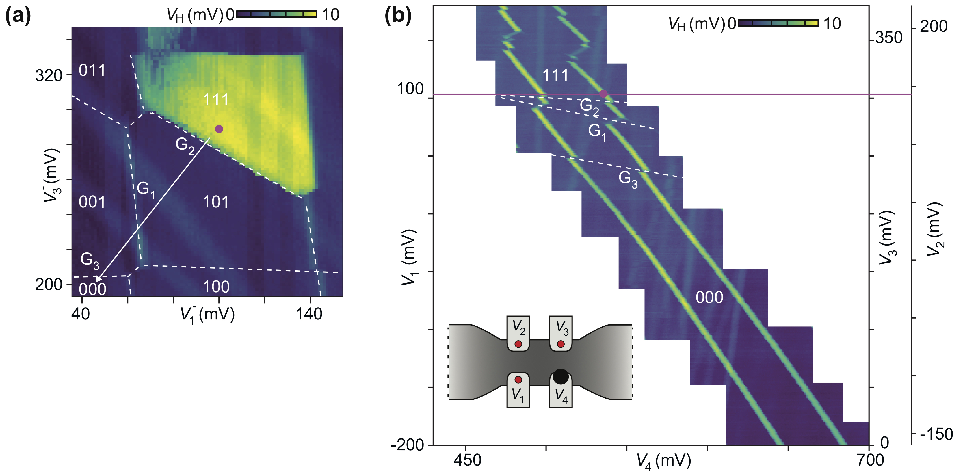
The compensated voltages are used to map out ground-state regions of various desired charge configurations of the qubit array. For example, Figure 2a was acquired by first parking and in the first Coulomb valley of dot 1 and dot 2 (keeping dot 3 empty by setting ), then tuning to the degeneracy point of dot 4 (maximum of ), before sweeping vs . The enhancement of clearly shows the extent of the 110 ground-state region. (Here, numbers indicate the occupation of the three qubit dots, as illustrated in the schematics of Fig. 2.) Due to the relatively large capacitive coupling of the sensor dot to the qubit dots, dot 4 is in Coulomb blockade outside the 110 region; there reduces to its approximately constant background. (The gain of the reflectometry circuit had been changed relative to the acquisition in Fig. 1d).
In addition to the transverse double dot in Fig. 2a, we also demonstrate the longitudinal (Fig. 2b) and diagonal (Fig. 2c) double dots. While such a degree of single-electron charge control is impressive for a reconfigurable, silicon-based multi-dot circuit, it is not obvious how coherent single-spin control (for example via micromagnetic field gradients Kawakami2014 or spin-orbit coupling Crippa2019 ) can most easily be implemented in these foundry-fabricated structures. One option is to encode qubits in suitable spin states of 111 triple dots, and operate these as voltage-controlled exchange-only qubits Medford2013 ; Russ2017 . To this end, we demonstrate in Fig. 2d the tune-up of a 111 triple dot (in order to populate also dot 2, was chosen more positive relative to Fig. 2c), revealing the pentagonal boundary expected for the exchange-only qubit Gaudreau2006 ; Medford2013 .
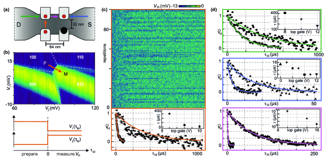
To demonstrate fast single-shot charge readout of the qubit array, we apply voltage pulses to G1-G3 while digitizing Volk2019a . Specifically, two-level voltage pulses are designed to induce one-electron tunneling events into the qubit array or within the array, as illustrated by color-coded arrows in Fig. 3a. One such pulse is exemplified in Fig. 3b, preparing one electron in dot 1 (P) before moving it to dot 2 (M). P and M are chosen such that the ground-state transition of interest (in this case the interdot transition) is expected halfway between P and M, using a pulse amplitude of 2 mV. This pulse is repeated many times, with fixed at a voltage that gives good visibility of the transition of interest in . Here, serves as a single-shot readout trace that probes for a tunneling event at time after the gate voltages are pulsed to the measurement point.
Figure 3d shows the repetition of 100 such readout traces obtained at a top gate voltage of 6 V, revealing the stochastic nature of tunneling events, in this case with an averaged tunneling time of 300 s. This time is obtained by averaging all single-shot traces and fitting an exponential decay. In the lower panel of Fig. 3c, indicates that the average (triangles) has been normalized according to the offset and amplitude fit parameters, which allows comparison with similar data (stars) obtained at a top gate voltage of 10 V (see Supplementary Information). The deviation of the data from the fitted exponential decay (solid line) may indicate the presence of multiple relaxation processes, and the reported decay times should therefore be understood as an approximate quantification of characteristic tunneling times within the array.
While the compact one-gate-per-qubit architecture in accurately-dimensioned Si-MOS devices may ultimately facilitate the wiring fanout of a large-scale quantum computer Franke2019 , an overall tunability of certain array parameters may initially be essential. Figure 3d reports averaged decays for the other transitions within the qubit array, phenomenologically demonstrating that various tunnel couplings within the array can be increased significantly by increasing the common top-gate voltage (insets).
An important resource for tunnel-coupled two-dimensional qubit arrays is the ability to move or even exchange individual electrons (and their associated spin states) in real space. In fact, a two-dimensional triple dot, as in our device, is the smallest array that allows the exchange of two isolated electrons (Heisenberg spin exchange, as demonstrated in linear arrays Maune2012 , requires precisely timed wavefunction overlap).
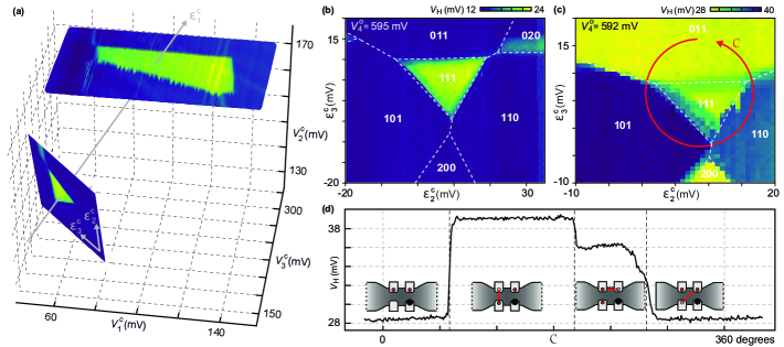
To demonstrate the spatial exchange of two electrons, we first follow the 111 ground-state region of Fig. 2d towards lower voltages on G1-3. In Figure 4a, this is accomplished by reducing the common-mode voltage , such that the 111 region only borders with two-electron ground states. In this gate-voltage region, the qubit array is most intuitively controlled using a symmetry-adopted coordinate system defined by
Physically, induces overall gate charge in the qubit array, whereas detuning () relocates gate charge within the array along (across) the silicon channel (cf. Fig. 1b). As expected from symmetry, the 111 region within the - control plane appears as a triangular region, surrounded by the three two-electron configurations 011, 101 and 110, as indicated by guides to the eye in Fig. 4b. Importantly, due to the finite mutual charging energies within the array (set by inter-dot capacitances), these three two-electron regions are connected to each other, allowing the cyclic permutation of two electrons without invoking doubly-occupied dots (wavefunction overlap) or exchange with a reservoir.
In principle, any closed control loop traversing 011101110011 should exchange the two electrons, which are isolated at all times by Coulomb blockade, making this a topological operation that may find use in permutational quantum computing Jordan2010 . In practice, leakage into unwanted qubit configurations (such as 111, 200, 020, etc) can be avoided by mapping out their ground-state regions, as demonstrated in Fig. 4c by slightly adjusting the operating point of the sensor dot. This sensor tuning also allows us to verify the sequence of qubit configurations while sweeping gate voltages along the circular shuttling path C, by simultaneously digitizing . The time trace of one shuttling cycle, starting and ending in 011, is plotted in Fig. 4d, and clearly shows the three charge transitions associated with the two-dimensional exchange (i.e. spatial permutation) of two electrons.
In this experiment, only gates G1, G2, and G3 can be pulsed quickly, due to our choice of wirebonding G4 as a reflectometry sensor. We verified that dot 4 can also be depleted to the last electron (see Supplementary Information), and future work will investigate whether the sensor dot can simultaneously serve as a qubit dot. Our choice of utilizing dot 4 as a charge sensor (read out dispersively from its gate) realizes a compact architecture for spin-qubit implementations where each gate in principle controls one qubit. This technique also alleviates drawbacks associated with the pure dispersive sensing of quantum capacitance, such as tunneling rates constraining the choice of rf carrier frequencies or significantly limiting the visibility of transitions of interest. For example, the honeycomb pattern in Fig. 1d with a clear visibility of dot-4 and dot-1 transitions is unusual for gate-based dispersive sensing in the few-electron regime, where small tunneling rates typically limit the visibility of dot-to-lead or interdot transitions Gonzalez-Zalba2015 . This is a consequence of the strong cross-capacitance between the reflectometry gate G4 and dot 1, allowing the rf excitation to probe also the quantum capacitances arising from dot 1. This also explains the observed discrete features within the bias triangles and shows the potential of gate-based reflectometry for directly revealing excited quantum dot states. The binary nature of the high-bandwidth charge signal (evident in Fig. 2) may also simplify the algorithmic tuning of qubit arrays Baart2016b .
While all data presented was obtained at zero magnetic field, application of finite magnetic fields to explore spin dynamics should also be possible Maurand2016 ; Urdampilleta2019 . We further expect significant improvements of the reflectometry signal by using superconducting inductors Ahmed2018 and Josephson parametric amplifiers Schaal2019 .
In conclusion, we demonstrate a two-dimensional array of quantum dots implemented in a foundry-fabricated silicon nanowire device. Each dot can be depleted to the last electron, and pulsed-gate measurements and single-shot charge readout via gate-based reflectometry allow manipulation of individual electrons within the array, while a common top gate provides an overall tunability of tunnel couplings. We demonstrate that the array is reconfigurable in situ to realize various multi-dot configurations, and utilize the two-dimensional nature of the array to physically permute the position of two electrons. These results constitute key steps towards fault-tolerant quantum computing based on scalable, gate-defined quantum dots.
I Acknowledgements
We thank Silvano De Franceschi for technical help and the coordination of samples. This project received funding from the European Union’s Horizon 2020 research and innovation programme under grant agreement MOS-quito (No. 688539). F.A. acknowledges support from the Marie Sklodowska-Curie Action Spin-NANO (Grant Agreement No. 676108). A.C. acknowledges support from the EPSRC Doctoral Prize Fellowship. F.K. acknowledges support from the Independent Research Fund Denmark.
References
- (1) Veldhorst, M. et al. A two-qubit logic gate in silicon. Nature 526, 410 (2015). eprint 1411.5760.
- (2) Muhonen, J. T. et al. Storing quantum information for 30 seconds in a nanoelectronic device. Nature Nanotechnology 9, 986 (2014).
- (3) Watson, T. F. et al. A programmable two-qubit quantum processor in silicon. Nature 555, 633–637 (2018).
- (4) He, Y. et al. A two-qubit gate between phosphorus donor electrons in silicon. Nature 571, 371 (2019).
- (5) Zajac, D. M. et al. Resonantly driven CNOT gate for electron spins. Science 359, 439–442 (2018).
- (6) Yoneda, J. et al. A quantum-dot spin qubit with coherence limited by charge noise and fidelity higher than 99.9%. Nature Nanotechnology 13, 102–106 (2018).
- (7) Mortemousque, P. A. et al. Coherent control of individual electron spins in a two dimensional array of quantum dots. eprint Preprint at https://arxiv.org/abs/1808.06180 (2018).
- (8) Dehollain, J. P. et al. Nagaoka ferromagnetism observed in a quantum dot plaquette. eprint Nature doi:10.1038/s41586-020-2051-0 (2020).
- (9) Betz, A. C. et al. Reconfigurable quadruple quantum dots in a silicon nanowire transistor. Applied Physics Letters 108, 203108 (2016).
- (10) Maurand, R. et al. A CMOS silicon spin qubit. Nature Communications 7, 13575 (2016).
- (11) Crippa, A. et al. Gate-reflectometry dispersive readout and coherent control of a spin qubit in silicon. Nature Communications 10, 2776 (2019).
- (12) Urdampilleta, M. et al. Gate-based high fidelity spin readout in a CMOS device. Nature Nanotechnology 14, 737–742 (2019).
- (13) Vandersypen, L. M. K. et al. Interfacing spin qubits in quantum dots and donors hot , dense , and coherent. npj Quantum Information 3, 34 (2017).
- (14) Barraud, S. et al. Development of a CMOS Route for Electron Pumps to Be Used in Quantum Metrology. Technologies 4, 10 (2016).
- (15) Hutin, L. et al. Gate reflectometry for probing charge and spin states in linear Si MOS split-gate arrays. eprint Preprint at https://arxiv.org/abs/1912.10884 (2019).
- (16) Chanrion, E. et al. Charge detection in an array of CMOS quantum dots. eprint Preprint at https://arxiv.org/abs/2004.01009 (2020).
- (17) Volk, C., Chatterjee, A., Ansaloni, F., Marcus, C. M. & Kuemmeth, F. Fast Charge Sensing of Si/SiGe Quantum Dots via a High-Frequency Accumulation Gate. Nano Letters (2019).
- (18) Kawakami, E. et al. Electrical control of a long-lived spin qubit in a Si/SiGe quantum dot. Nature Nanotechnology 9, 666 (2014).
- (19) Medford, J. et al. Self-consistent measurement and state tomography of an exchange-only spin qubit. Nature Nanotechnology 8, 654 (2013).
- (20) Russ, M. & Burkard, G. Three-electron spin qubits. Journal of Physics: Condensed Matter 29, 393001 (2017). eprint 1611.04945.
- (21) Gaudreau, L. et al. Stability Diagram of a Few-Electron Triple Dot. Physical Review Letters 97, 036807 (2006).
- (22) Franke, D. P., Clarke, J. S., Vandersypen, L. M. K. & Veldhorst, M. Rent’s rule and extensibility in quantum computing. Microprocessors and Microsystems 67, 1–7 (2019).
- (23) Maune, B. M. et al. Coherent singlet-triplet oscillations in a silicon-based double quantum dot. Nature 481, 344–347 (2012).
- (24) Jordan, S. P. Permutational Quantum Computing. Quantum Information and Computation 10, 470 (2010).
- (25) Gonzalez-Zalba, M. F., Barraud, S., Ferguson, A. J. & Betz, A. C. Probing the limits of gate-based charge sensing. Nature Communications 2, 1–8 (2015).
- (26) Baart, T. A., Eendebak, P. T., Reichl, C., Wegscheider, W. & Vandersypen, L. M. K. Computer-automated tuning of semiconductor double quantum dots into the single-electron regime. Applied Physics Letters 108, 213104 (2016).
- (27) Ahmed, I. et al. Radio-Frequency Capacitive Gate-Based Sensing. Physical Review Applied 10, 014018 (2018).
- (28) Schaal, S. et al. Fast Gate-Based Readout of Silicon Quantum Dots Using Josephson Parametric Amplification. Physical Review Letters 124, 067701 (2020).
- (29) eprint Electronic access: https://www.qdevil.com.
II Supplementary Information
II.1 Sample fabrication
Our quantum-dot arrays are fabricated at CEA-LETI using a top-down fabrication process on 300-mm silicon-on-insolator (SOI) wafers, adapted from a commercial fully-depleted SOI (FD-SOI) transistor technology Barraud2016 . Compared to single-gate transistors (in which a single gate electrode wraps across a silicon nanowire) two main changes in regards to gate patterning are needed in order to realize 2xN arrays. First, N gate electrodes are patterned, in series along one silicon channel. Second, a dedicated etching process is introduced that creates a narrow trench through the gate electrodes, along the nanowire, thereby splitting each gate electrode into one split-gate pair Houtin2019 . The main fabrication steps are described below. For illustrative purposes, the device shown in Fig. 1a was imaged after gate patterning and first spacer deposition Barraud2016 , and does not represent the top gate and back-end.
Starting with a blank SOI wafer (12 nm Si / 145 nm SiO2), the active mesa patterning is performed in order to define a thin, undoped nanowire via a combination of deep-ultra-violet (DUV) lithography and chemical etching. The silicon nanowire is 7-nm thin after oxidation, and has a width of approximately 70 nm for the device studied in this work. Then, a high-quality 6-nm thick SiO2 gate oxide is deposited via thermal oxidation. To define the metal gate, a 5-nm thick layer of TiN followed by 50 nm of n+ doped polysilicon is used from the standard FD-SOI processing. The gate is patterned using a combination of conventional DUV lithography combined with an electron-beam lithography process, allowing to achieve an aggressive intergate pitch down to 64 nm (gate length, longitudinal gate spacing, and transverse gate spacing as small as 32 nm). Then, 35-nm thick SiN spacers between gates and between gates and source/drain (S/D) regions are formed, which serve two roles: They protect the intergate regions from self-aligned doping (therefore keeping the channel undoped), and they define tunnel barriers within the array. Afterwards, raised S/D contacts are regrown to 18 nm to reduce access resistance. Then, to obtain low access resistances, S/D are doped in two steps: first with lightly-doped drain (LDD) implant (using As at moderate doping conditions) and consecutive annealing to activate dopants, and then with highly-doped drain (HDD) implant (As and P at heavy doping conditions). To complete the device fabrication, the gate and lead contact surfaces are metalized to form NiPtSi (salicidation), in preparation for metal lines to be routed to bonding pads on the surface of the wafer. Finally, a standard copper-based back-end-of-line process is used to define an optional metallic top gate 300 nm above the nanowire, to make interconnections to bonding pads, as well as to encapsulate the device in a protective glass of siliconoxide. Using the powerful parallelism of top-down fabrication, we obtain dozens of dies on a single 300-mm-diameter wafer, each of them containing hundreds of quantum-dot devices buried 2-3 m below the chip surface.
II.2 Voltage control
Low-frequency control voltages are generated by a multi-channel digital-to-analog converter (QDevil QDAC) QDevil , whereas high-frequency control voltages are generated using a Tektronix AWG5014C arbitrary waveform generator. To acquire voltage scans that involve compensated control voltages, we use appropriately programmed QDevil QDACs.
II.3 Radio-frequency reflectometry
The reflectometry technique is similar to that described in Ref. Volk2019a , in which a sensor dot tunnel-coupled to two reservoirs was monitored via a SMD-based tank circuit wirebonded to the accumulation gate of the sensor. In this work, the sensor dot (located underneath G4) is tunnel-coupled only to one reservoir (source in Fig. 1a), and the increased cross-capacitance to the three qubit dots results in much larger electrostatic shifts of dot 4 whenever the occupation of the qubit dots changes. For example, each pair of triple points in Fig. 1d is spaced significantly larger than the peak width associated with the sensor-dot transition.
In order to increase the signal intensity as well as to allow for inaccuracies in , we find it useful to occupy the sensor dot with several electrons (6-9 in Fig. 2), and to intentionally power-broaden the Coulomb peaks of dot 4 (with -70 dBm applied to the inductor) for all acquisitions in Fig. 2. The SMD inductance used is 820 nH, and the rf carrier has a frequency of a 191.3 MHz.
For the real-time detection of interdot tunneling events in Fig. 3c, an Alazar digitizing card (ATS9360) is used with a sample rate set to 500 kS/s. The integration time per pixel is set by a 30 kHz low-pass filter (SR560), yielding a signal-to-noise ratio as high as 1.4 in this device.
x
II.4 Determination of electron number
For a given tuning of the qubit array, the occupation number of each qubit dot is determined by counting the number of discrete electrostatic shifts of the sensor dot (i.e. shifts of a dot-4 Coulomb peak in along ) as the qubit array is emptied by continuously reducing the control voltage of the dot of interest. If the total number of electrons within the qubit array is desired, all three qubit voltages can be reduced simultaneously, while sweeping over one or more Coulomb peaks of dot 4, which serves as an electrometer. An example of such a diagnostic scan, for the case of a 111-occupied triple dot, is shown in Figure S1. To determine the number of electrons in the sensor (dot 4), we utilized Coulomb peaks associated with dot 1 as an electrometer for dot 4, while continuously reducing . This works because the strong dispersive signal associated with the dot-1-to-lead transition shows discrete shifts (along ) whenever the dot-4 occupation changes (note the large shifts of the dot-1 transition induced by dot 4 in Fig. 1d).
II.5 Capacitance matrix
To support our interpretation of dot i being localized predominantly underneath gate i (i=1…4), we extract from stability diagrams the capacitances between gate j and dot i (in units of aF):
In this capacitance matrix, the relatively large diagonal elements reflect the strong coupling between each gate and the dot located underneath it. By adding several electrons to the array, we have also observed that the capacitances change somewhat, indicating a spatial change of wavefunctions (not shown) and suggesting an alternative way to change tunnel couplings.
II.6 Fitting tunneling times
In Figure 3c we show 100 single-shot traces (upper panel) and the average of all traces. The average has been fitted by an exponential decay with the initial value, the 1/e time, and the long-time limit (offset) as free fit parameters. For plotting purposes, is then calculated by substracting the offset from the average, and dividing the result by the initial value. For clarity of presentation (the sampling rate for raw data of Fig. 3c was 500kS/s), in the lower panel of Fig. 3c we also decimated the time bins by a factor of 4.