Current address: ]Quantum Motion Technologies, Windsor House, Cornwall Road, Harrogate HG1 2PW, U.K.
Large dispersive interaction between a CMOS double quantum dot and microwave photons
Abstract
We report fast charge state readout of a double quantum dot in a CMOS split-gate silicon nanowire transistor via the large dispersive interaction with microwave photons in a lumped-element resonator formed by hybrid integration with a superconducting inductor. We achieve a coupling rate MHz by exploiting the large interdot gate lever arm of an asymmetric split-gate device, , and by inductively coupling to the resonator to increase its impedance, . In the dispersive regime, the large coupling strength at the double quantum dot hybridisation point produces a frequency shift comparable to the resonator linewidth, the optimal setting for maximum state visibility. We exploit this regime to demonstrate rapid dispersive readout of the charge degree of freedom, with a SNR of 3.3 in 50 ns. In the resonant regime, the fast charge decoherence rate precludes reaching the strong coupling regime, but we show a clear route to spin-photon circuit quantum electrodynamics using hybrid CMOS systems.
I Introduction
Electron spins in silicon quantum dots are promising candidates for large-scale quantum computation Zwanenburg et al. (2013). Their long coherence times enable high-fidelity single- and two- qubit gates Yoneda et al. (2018); Yang et al. (2019); Huang et al. (2019); Xue et al. (2019); Zajac et al. (2018) and their compatibility with industrial manufacturing processes Hutin et al. (2018); Pillarisetty et al. (2019); Zwerver et al. (2021) facilitates the fabrication of large quantum dot arrays, and their integration with classical electronics Schaal et al. (2019). All quantum computing architectures aiming to achieve fault tolerance Fowler et al. (2012) require high-fidelity quantum state readout. To implement quantum error correction (QEC), this readout must be achieved in time scales significantly shorter than the coherence time of the qubits ( ms Veldhorst et al. (2014)), and ideally faster than the time scales of single- and two-qubit gates to avoid becoming the bottleneck in error-correction cycles. For the highest fidelity gates, these timescales are sub-s Yang et al. (2019) and 5 s Huang et al. (2019), respectively. Renewed efforts have been directed at achieving this goal using charge sensors combined with amplification at the millikelvin stage Curry et al. (2019) or with radio-frequency techniques Urdampilleta et al. (2019); Volk et al. (2019), reaching a promising 97% fidelity in s Keith et al. (2019).
Circuit quantum electrodynamics (cQED) provides an alternative readout approach which removes the necessity for a charge sensor and simplifies the qubit architecture Blais et al. (2004a); Wallraff et al. (2004); Blais et al. (2020). The qubit interacts with photons in a detuned microwave cavity whose eigenfrequencies are modified conditional on the qubit state. Recent results have demonstrated this is a competitive approach for silicon spin qubits and have reached fidelities of 73% in 2.6 ms West et al. (2019) and 82.9% in 300 s Pakkiam et al. (2018), when using hybrid resonant circuits, and 98% in 6 s, when using on-chip resonators Zheng et al. (2019). Although on-chip integration has enabled faster readout, it poses an important challenge for the future development of compact nanometre-scale spin qubit arrays, given that current microwave resonator designs have characteristic length scales of the order of m Samkharadze et al. (2018); Stockklauser et al. (2017). Hybrid multi-chip modules give freedom to optimise the layout of the qubit layer without the spatial constraints of the microwave electronics and are likely to facilitate the development of two-dimensional qubit arrays Veldhorst et al. (2017); Li et al. (2018), a requirement for the implementation of the surface code QEC Fowler et al. (2012). However, the technology to achieve readout times compatible with QEC using hybrid multi-chip modules requires further development.
In this paper, we demonstrate fast charge state readout of a complementary-metal-oxide-semiconductor (CMOS) double quantum dot (DQD) coupled to a high-impedance lumped-element resonator. We measure an interdot charge transition with a signal-to-noise ratio (SNR) of 3.3 in just 50 ns. The signal, which represents that of a singlet outcome in singlet-triplet readout schemes, should enable high-fidelity spin readout in sub-s time scales. Our large signal is achieved by increasing the charge-photon coherent coupling rate to MHz, comparable to those reported in fully-integrated circuits Stockklauser et al. (2017); Samkharadze et al. (2018). The large coupling results directly from exploiting the large interdot gate lever arm of an asymmetric split-gate device, , and from inductively coupling to the resonator to increase its impedance. It allows us to operate the system in the intermediate dispersive regime, where the dispersive frequency shift of the microwave cavity, , is as large as the photon decay rate, ; the condition for maximum state visibility Schuster (2007). Furthermore, we show the scalability of the architecture by simultaneously reading two resonators, each of them containing a quantum dot device, via frequency multiplexing. Finally, by tuning the charge configuration of the DQD, we reach the resonant regime of cQED, where the qubit and resonator energies match. Although , the fast decay rate of the charge degree of freedom of the DQD precludes reaching the strong coupling limit in this experiment. By coupling to the long-lived spin degree of freedom Ciriano-Tejel et al. (2021), it may be possible to reach the strong coupling limit, which has been achieved in Si/SiGe heterostructures Samkharadze et al. (2018); Mi et al. (2018), but not yet in Si/SiO2 systems. We note that the microwave circuitry presented here should readily improve the readout fidelity not only of CMOS-based devices but of any semiconductor-based system, especially those with a large gate lever arm such as topological qubits de Jong et al. (2019); Sabonis et al. (2019).
II Architecture
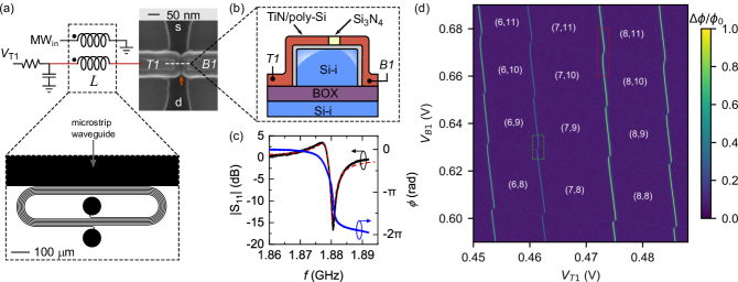
Our multi-module assembly consists of a silicon chiplet and a superconducting chiplet, connected via wire-bonds. The superconducting chiplet contains an elongated spiral inductor and a 50 microstrip waveguide, fabricated using optical lithography from an 80 nm thick sputter-deposited NbN film on a sapphire substrate, shown in Fig. 1(a). The structure is designed to allow microwave radiation to be inductively coupled into the inductor from the waveguide. We connect the inner bond pad of the inductor to the T1 gate of an -type split-gate silicon-on-insulator nanowire field-effect transistor (NWFET), see Fig. 1(b), and the outer bond pad to a bias-tee to enable DC gating. More details of the circuit can be found in Appendix B.
The intrinsic-Si body of the nanowire, with a height of 7nm and width 70 nm, is covered by 6 nm SiO2 gate oxide and separated from the silicon substrate by a 145 nm buried oxide. Two gates, arranged face-to-face, wrap around the sides and part of the top surface of the nanowire. The gates have a length along the nanowire of 60 nm, and surrounding the gates the nanowire is covered by 34 nm Si3N4 spacers. The gap between the gates at the top of the nanowire is 40 nm wide, and is also covered by Si3N4 Lundberg et al. (2020). An orange arrow on the top-down SEM image, Fig. 1(a), highlights the gap between the gates. We connect the inductor to the gate with the larger overlap to make use of the larger interdot gate lever arm, as we will see later. Under the appropriate bias, a DQD forms within the corners of the NWFET, as illustrated in Fig. 1(b) Betz et al. (2015). We model a single valence electron in the DQD as a coupled two-level system with eigenfrequencies where is the tunnel coupling and is the frequency detuning between dots.
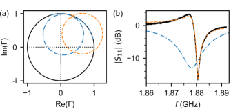
The combined inductor-DQD system forms an resonant circuit. We study the properties of the resonator by monitoring the amplitude and phase of the reflected signal when applying a microwave tone to the microwave input line, MW, with the NWFET grounded at 12 mK, see Fig. 1(c). We find a resonance at = 1.88 GHz, which can be fitted using a complex external Q-value (see red dashed line in Fig. 1(c)) Wisbey et al. (2010); Khalil et al. (2012). From the fit and our experimentally measured inductance value nH Ahmed et al. (2018), we deduce a total parasitic capacitance fF, a characteristic impedance , an internal (external) decay rate MHz ( MHz) and a total photon decay rate of MHz. Moreover, we plot the phase shift across the resonance (blue trace) and observe a phase shift confirming that photons predominantly escape the resonator before decaying Ibberson et al. (2019).
Next, at fixed frequency, we monitor the phase shift of the reflected signal as a function of the gate biases and , see Fig. 1(d). An enhancement of the phase signal in a quasi-periodic honeycomb pattern is clearly visible. The lines correspond to charge bistable regions in a DQD where the charge susceptibility of the DQD is non-zero Mizuta et al. (2017); Benito et al. (2017). We infer the electron population in each quantum dot by using a visible dot-to-reservoir transition of one dot as a charge sensor of the other dot, see Appendix D. Then we invert the role of the dots and count the number of electrons in the opposite dot Lundberg et al. (2020). The numbers in parentheses in Fig. 1(d) indicate the number of electrons on the dot under the (T1, B1) gates. Interdot charge transitions (ICTs) at intersections of the horizontal and vertical lines are not visible for electron populations smaller than those presented on this plot, indicating insufficient wavefunction overlap for tunneling to occur in the timescale of the resonator period Gilbert et al. (2020).
In the remainder of this paper, we focus on studying the interaction between the resonator and the DQD. We use two ICTs with different tunnel couplings to access two different regimes. First, the dispersive regime, where the qubit frequency is greater than the resonator frequency, which we use to achieve fast readout of the charge state (red dotted box in Fig. 1(d)) and second, the resonant regime, where the qubit and resonator frequencies are equal (green dashed box in Fig. 1(d)).
III Large dispersive interaction
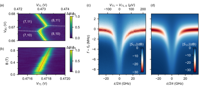
We bias the DQD to the ICT between charge states (7,11) and (8,10), see Fig. 2(a). The ICT and the T1 dot-to-reservoir (DTR) lines are visible, but the B1 DTR ones are not because of the weak lever arm of the T1 gate to the B1 dot. We focus on the ICT and extract the interdot gate lever arm from the voltage shift of the transition as the magnetic field is increased, see Fig. 2(b). For an even parity transition such as this, where the total number of valence electrons is even (for example a transition), the position of the ICT shifts with a slope determined by , where is the electron -factor and is the Bohr magneton Mizuta et al. (2017). The signal at T originates from charge transitions between states with different spin numbers. The reason for spin transitions occurring under the microwave electric field is unknown, but could potentially be explained by electrically driven Landau-Zener transitions followed by a fast relaxation hotspot near the point of anticrossing Yang et al. (2013). We obtain . The large is a direct consequence of the large asymmetric channel overlap of T1 and represents the highest reported for any silicon device. Previous measurements of a device from the same wafer used the gate electrode with the smaller overlap (B1) which yielded Lundberg et al. (2020). Achieving a large is of great importance for cQED architectures since it relates directly to the dipole moment of the quantum system and hence to the coherent coupling constant , where is the resistance quantum Childress et al. (2004).
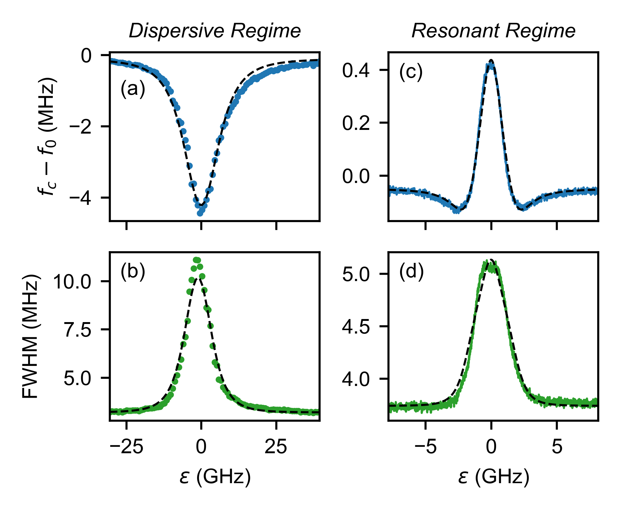
To explore the interaction between the resonator and the DQD, we measure the reflected spectrum of the resonator as we change the DQD frequency detuning, , via , see Fig. 2(c). We apply the input signal with a power of -125 dBm at , well below the onset of power broadening. At , the resonator exhibits a maximum frequency shift with respect to the bare resonator frequency, MHz. This value is comparable to the bare cavity linewidth . In addition, we observe an increase in the effective resonator linewidth, , which we attribute to the interaction of the resonator with a fast decaying DQD, as we shall confirm later.
To extract the relevant parameters of the resonator-DQD system, and to simulate the response, we model the DQD as a coupled two-level system, and the microwaves by a weak periodic field Petersson et al. (2012). In the rotating-wave approximation, we obtain the effective Hamiltonian
| (1) |
where , , , is the inversion operator, are the raising and lowering operators of the DQD and and are the photon annihilation and creation operators. We use the input operator formalism and develop the Heisenberg-Langevin equations of motion to obtain the reflection coefficient in the steady state when neglecting quantum noise contributions
| (2) |
where is the reflected power ratio, is the susceptibility of the DQD and is the DQD decay rate. We use Eq. 2 to simulate the experimental results, see Fig. 2(d). From the -dependent shift in the resonance frequency, , and the resonance linewidth increase , see Appendix A, we determine the relevant system parameters: MHz, GHz and GHz. From these values, we can draw some important conclusions. Firstly, the DQD presents a fast decay rate, in line with reports in the literature for the charge degree of freedom in silicon MOS structures Dupont-Ferrier et al. (2013); Gonzalez-Zalba et al. (2016); Chatterjee et al. (2018). We discard Purcell-enhanced relaxation, 3.7 kHz Blais et al. (2004b), and measurement-induced decoherence due to photon shot noise, MHz Yan et al. (2016) (where is the average photon number) as the cause of the large , and instead attribute it to charge noise at the Si/SiO2 interface. Secondly, although , we note that the coupling strength is much greater than the resonator linewidth (i.e. ) and hence our system satisfies one of the requirements to reach the strong coupling regime. Finally, since and , our measurements are in the intermediate dispersive limit, relevant for high-fidelity qubit readout.
IV Dispersive Readout Performance
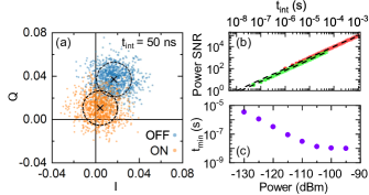
We now evaluate the dispersive readout performance by measuring the signal-to-noise ratio (SNR) of the charge transition as a function of integration time, . Using a continuous-wave excitation, we measure the and demodulated components of the reflected signal at the two voltage positions marked in Fig. 2(a); the Coulomb blockaded region (blue cross) and the charge degenerate regime (orange cross). This corresponds to the expected signal in a singlet-triplet spin readout scheme West et al. (2019), in the limit where the valley splitting is larger than the tunnel coupling. Measurements of the valley splitting in excess of eV have been reported for corner dots in the single-electron regime Ciriano-Tejel et al. (2021) which is much larger than the tunnel coupling measured in this work, eV. As shown in Fig. 3(a), the distributions of points at the two voltages are separated in the plane. We use this data to calculate the power SNR, given by , where is the distance between the centers of the clusters (marked by black crosses), and is the average standard deviation of the two states (dotted circles). In Fig. 3(b), the red and green dots plot the SNR for two instrument configurations, using either a 1 MHz or 20 MHz maximum measurement bandwidth respectively. From a linear fit to the data, we extract , defined as the integration time for which SNR = 1. At the optimal input power of -100 dBm (see Fig. 3(c)), for the 1 MHz data we find ns. This value is shorter than other silicon implementations which have benefited from either a Josephson Parametric Amplifier (JPA) Schaal et al. (2020), or a fully-integrated resonator Zheng et al. (2019). Our result is comparable to the best reported in any dispersively detected semiconductor quantum dot, which was obtained in InAs and utilised a JPA Stehlik et al. (2015). Furthermore, following a simple readout fidelity model Barthel et al. (2009), we obtain a 99.7% electrical readout fidelity in 300 ns. Using the 20 MHz bandwidth configuration (green dots), we can experimentally access integration times down to 50 ns. We note that the lower SNR in the 20 MHz case is due to the comparably larger equivalent noise bandwidth of the filtering system. We measure an SNR of 3.3 at ns, for which the data is plotted in Fig. 3(a). This result agrees well with the estimated SNR in the intermediate dispersive regime 2.6, where is the Boltzmann constant and K is the noise temperature of the cryogenic amplifier, see Appendix F.
Finally, we highlight that this architecture can be easily extended to read out several qubits from a single transmission line by adding additional spirals along the length of the microstrip waveguide and employing frequency-multiplexing techniques Hornibrook et al. (2014); Heinsoo et al. (2018). We simultaneously read the charge states of two separate NWFETs embedded in resonators of different frequencies (1.8 GHz and 2.4 GHz, corresponding to superconducting inductors with nH and nH respectively), see Appendix C for experimental details.
V Resonant regime
In our split-gate geometry, we are not able to tune the tunnel coupling independently, however can vary with electron occupation. We bias the DQD to a different ICT (highlighted by the green dashed rectangle in Fig. 1(d)) and investigate the effect of the DQD on the resonator in this case. In Fig. 4(a), we measure the resonator’s frequency spectrum as we vary across the transition, and observe a substantially different response with respect to the dispersive regime (also note the reduced span of the horizontal axis). In this case, close to , the resonator’s frequency increases as opposed to the previous configuration. In addition, we again observe an increase of the effective resonator linewidth . We attribute these effects to the qubit and the resonator becoming resonant at some where . However, due to the a large DQD decay rate, we are unable to observe the vacuum Rabi mode splitting characteristic of the strong coupling regime. To confirm our hypothesis, we repeat the process described in Appendix A to fit the data. Using the lever arm measurement , obtained from magnetospectroscopy of this ICT, we find a coupling strength MHz, tunnel coupling MHz and decay rate GHz. The smaller lever arm accounts for part of the reduction in compared with the dispersive regime, and a further reduction may be linked to the smaller tunnel coupling, analogous to the dependence of the coherent coupling rate on Josephson energy for superconducting qubits Koch et al. (2007). The reduced in comparison to the dispersive regime can be understood by assuming phonon-mediated relaxation dominates, for which Boross et al. (2016). Our simulations confirm that the system reaches the resonant regime since the tunnel coupling is lower than the frequency of the resonator. Furthermore, the simulation confirms that the fast decay rate of the DQD prevents us observing the strong coupling limit.
VI Conclusion
We have presented a multi-module integrated circuit for fast readout of the charge state of quantum dot devices enabled by a large charge-photon coupling rate. In our demonstration, the enhanced coupling results from two critical improvements. First, the large interdot gate lever arm which arises from the thin gate oxide, the thin silicon-on-insulator layer, and the asymmetric gate overlap of the nanowire. Second, the enhanced resonator impedance due to the reduced capacitance of the resonator, achieved by coupling inductively rather than capacitively Ahmed et al. (2018); Schaal et al. (2020); Ibberson et al. (2019). In the dispersive regime, we achieve a frequency shift of the order of the resonator bandwidth, , the condition for maximum state visibility. Furthermore, the measured coupling rate is greater than the resonator linewidth, satisfying one of the requirements for strong coupling. Future experiments aiming to achieve strong coupling to the charge degree of freedom in multi-module quantum systems should focus on decreasing the DQD charge decay rate. One strategy to do this is to move to high-mobility heterostructures where lower have been demonstrated Mi et al. (2017); Scarlino et al. (2019), possibly because of the reduced charge noise when compared to Si/SiO2 interfaces. However, achieving a high in those systems is a complex technical challenge because of the typically large separation between the gates and the quantum dot. Alternatively, coupling to the spin rather than the charge degree of freedom should provide an optimal route to cQED in hybrid superconducting-CMOS systems, particularly if hole-based devices, which are subject to sizable spin-orbit coupling, are used Crippa et al. (2019); Maurand et al. (2016). Our work shows that, in the short term, it will be possible to reach the large coupling rates necessary for cQED without the necessity to integrate microwave resonators in a CMOS process. In the long-term, asymmetric gate designs made out of high kinetic inductance materials, like TiN, inductively coupled to a single input line, should provide a more scalable route to integrated CMOS cQED. Furthermore, if the large of CMOS DQDs were combined with even higher impedance resonators, it will be possible to access the ultrastrong coupling regime Forn-Díaz et al. (2019). We note that to achieve the fast readout presented in this paper, we did not use a JPA showing that there is room for further improvement. Finally, we expect that our approach should impact research aiming at improving the readout fidelity of Majorana-based quantum devices de Jong et al. (2019); Sabonis et al. (2019).
VII Acknowledgments
This research has received funding from the European Union’s Horizon 2020 Research and Innovation Programme under Grant Agreement No. 688539 (http://mos-quito.eu). M.F.G.Z. aknowledges support from the Royal Society and the Winton Programme of the Physics of Sustainability. D.J.I is supported by the Bristol Quantum Engineering Centre for Doctoral Training, EPSRC Grant No. EP/L015730/1. T.L. and G.A.O. acknowledge support from EPSRC Cambridge NanoDTC EP/L015978/1 and L.C. acknowledges support from EPSRC Cambridge UP-CDT EP/L016567/1.
Appendix A S-parameter analysis and fitting
For the analysis of the frequency spectrum of the DQD-resonator in Fig. 2 and Fig. 4 in the main paper, it becomes particularly useful to represent Eq. 2 in the form of a complex Lorentzian
| (3) |
where is the resonant angular frequency of the resonator and the center frequency is given by
| (4) |
and the effective linewidth of the resonator by
| (5) |
In the limit , Eq. 4 presents full-width-at-half-maximum in given by .
We now describe our method for extracting the coherent coupling rate , tunnel coupling , and charge relaxation rate from the frequency spectroscopy data, see Fig. 2(c) for the dispersive regime, and Fig. 4(a) for the resonant regime. For each step in the detuning , we extract the resonance frequency and the FWHM of the resonance. In Fig. A1 we plot and the FWHM in panels (a) and (b) respectively for the dispersive regime, and (c) and (d) respectively for the resonant regime. We then fit these peak shapes using Eq. 4 for and Eq. 5 for the FWHM. For best accuracy, we fit simultaneously and FWHM with common parameters , and . Fitting is performed using orthogonal distance regression (ODR), taking into account errors on both and axes for each plot. The dominant error on stems from the uncertainty in , and the errors on and the FWHM are given by the nonlinear least-squares fits used to extract their values from the data. The errors quoted on the fitted parameters, , , and , are obtained from the covariance matrix of the ODR fit. The quality of the resulting fits, indicated by the black dashed lines, gives high confidence in the calculated parameters.
Appendix B RF circuit design and operation
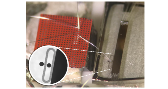
We present a photograph of the hybrid integrated system described in the main paper, showing the silicon NWFET and superconducting inductor on separate substrates, see Fig. A2. The T1 gate of the silicon CMOS transistor is connected to the centre of the NbN spiral inductor on the adjacent sapphire substrate, using an Al wire of length m and diameter m. An on-PCB bias-tee, not shown, is wire-bonded to the outer bond-pad of the spiral inductor, with an Al wire of similar length. The 50 microstrip waveguide runs approximately vertically on the right of the figure. The insert magnifies the elongated 6-turn spiral inductor which is separated from the microstrip waveguide by a m gap; the overall inductor footprint is m, including bond-pads.
The high impedance of the silicon NWFET split-gate is impedance-matched to the 50 microstrip waveguide, by embedding the device in an LC resonator and designing the distance between the spiral and the waveguide to achieve critical inductive coupling. The bias-tee capacitor (NPO COG 100 pF high-Q) acts as a short-circuit at the resonant frequency, thereby allowing high quality factors to be achieved by isolating the bias-tee resistor.
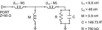
We now present two models of the resonant system formed by the NWFET, PCB, superconducting chiplet and bond wires, and attempt to reproduce the reflected spectrum data in Fig. 1(c). The first model consists of lumped elements only, illustrated in Fig. A3. In the second model, we use the Cadence® AWR® AXIEM® planar method-of-moments (MoM) software to simulate the NbN/sapphire/grounded-metal structure, which is then embedded in a lumped-element circuit representing the other structures that is simulated using Cadence® AWR® Microwave Office®, see Fig. A4.
In the first model, the coupled inductances of the NbN waveguide and spiral are represented using a T-circuit of inductors (see Fig. A3), where the central shunt inductance equals the mutual inductance, , and the left and right inductors are the stray inductances of the waveguide and spiral respectively, where is the inductance of the waveguide and is the spiral inductance. The capacitance, , that completes the resonator includes the self-capacitance of the spiral, the gate capacitance of the NWFET, and the total parasitic capacitances to ground. The resistor, , accounts for internal losses, namely dielectric losses of the two substrates and resistance of non-superconducting metals in the bias tee. We find from MoM simulations of the sapphire chip that nH, and deduce from our experimentally measured value of the spiral inductance (equal to ) that nH. The remaining parameters are then obtained by fitting the model to the data in Fig. 1(c) with and fixed. The asymmetry of the data is accounted for by including an additional parameter in the fit function, specifying the angle of rotation in the complex plane about the point marked by an orange X in Fig. A5(a). This rotation is caused experimentally by interference of the radiation reflected from the resonator with radiation reflected at other boundaries, in this case most likely the grounded end of the waveguide Khalil et al. (2010); Sage et al. (2011). Note that this model does not include the bias tee, making the assumption that it acts as a perfect ground in the vicinity of the resonant frequency.
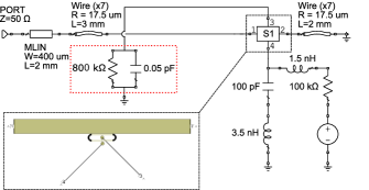
In the second model, we construct a planar model of the sapphire chip including, from bottom to top, the grounded metal plane on top of the PCB, the sapphire of thickness 500 m and dielectric constant 11.58, and the NbN microstrip and spiral. We model the NbN film as a perfect conductor with sheet inductance 1.35 pH/ to account for kinetic inductance, similar to other estimates Hayashi et al. (2014). This value was obtained by matching the simulated to the experimental resonant frequency of the un-bonded spiral, which was measured at 3.04 GHz. Wire bonds are also modelled in the MoM simulation in order to connect the spiral to the off-chip elements. Connected to the outer bond-pad via one of these wires is the bias tee, consisting of a 100 pF capacitor to ground, and a 100 k resistor through which the bias is applied. In addition, two inductors of a few nH each are included to model PCB tracks and thru-holes. Connected to the inner bond-pad of the spiral, are a resistor and capacitor in parallel to model the NWFET, similar to the previous model. We find that, to match the experimental resonant frequency, this capacitance must be reduced to fF, indicating that the majority of the 150 fF of the lumped-element model originates from the superconducting spiral. Moreover, separate simulations of the un-bonded spiral also show that its capacitance is approximately 100 fF, which could be reduced in future experiments Peruzzo et al. (2020). We have investigated the effects of different lengths of the bond-wires, which each contribute approximately 2 nH of inductance. For the bond-wire between spiral and NWFET, varying its length 50 produces 5 variation in the resonant frequency. A 50% variation in the length of the bond-wire between the spiral and the bias-tee shifts the resonant frequency by 3. No significant changes to the resonance width or depth were observed.
The simulated reflection spectra of the two models are compared with the experimental data in Fig. A5(b). The lumped-element model shows excellent agreement with the data, whereas for the MoM simulation, while its resonant frequency is close to the experiment, the width is overestimated. This can be attributed to our choice of value for the resistor modelling internal losses, for which we have used a value similar to the lumped-element model. This value is clearly an underestimate, from which we can conclude that the internal losses of the spiral predicted by the the MoM simulation have added a significant contribution. Note that varying the bias tee capacitor and resistor values by their rated tolerances has no visible effect. The MoM simulation also does not reproduce the asymmetry of the data.
Appendix C Frequency multiplexing
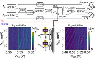
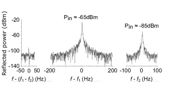
We fabricated a second NbN-on-sapphire chip that included multiple inductors close to the microstrip waveguide for frequency multiplexing experiments. Each inductor was wire-bonded to separate bias-tees and single-gate CMOS devices in the same configuration as before, enabling simultaneous measurement of two independent silicon quantum dots via the single microwave line. A 47 nH spiral inductor was bonded to a NWFET with gate length (L) 50 nm and width (W) 30 nm (device 1), and a 29 nH inductor was wire bonded to a NWFET with dimensions 50 nm (L) x 60 nm (W) (device 2), giving resonant frequencies at GHz and GHz respectively. A two-tone probe signal was synthesised by combining and from individual microwave generators and applied to the microstrip waveguide via an unattenuated coaxial line in our dilution refrigerator, see Fig. A6. The reflected signal was amplified at room temperature, split into two channels, and then demodulated separately with the generated and tones. By manipulating the gate and bias voltages of the two NWFETs at the same time, we simultaneously acquired the two Coulomb diamond plots shown in Fig. A6. We quantify the crosstalk between the two measurements by measuring the signal power of the intermodulation product at , see Fig. A7. It is not possible to observe the intermodulation product above the noise floor when applying the same input powers used to acquire the Coulomb diamonds, however, increasing the power of the tones resulted in an observable intermodulation product, at least 60 dB (40 dB) below the reflected () tones. The power of the intermodulation product is independent of the devices’ gate voltages, indicating that there is no crosstalk at the resonator-device level.
Using separate microwave generators is practical in “proof-of-principle” experiments requiring two or three frequencies, however, future experiments should focus on exploiting techniques used in software defined radio, where a multi-frequency signal is synthesised using digital signal processing, before being up-converted to microwave frequencies using a mixer and a reference source Jerger et al. (2012).
Appendix D Electron population
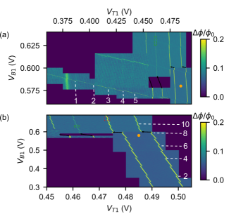
Here we present the data used to determine the electron population of the DQD. In Fig. A8(a), we zoom in on a charge transition of the B1 dot and count the discontinuities which indicate loading of electrons into the T1 dot, marked by the white dashed lines. No discontinuities are observed at V, so we conclude that the first shown here, occurring at V, corresponds to the first electron loaded into the T1 dot. In Fig. A8(b), we follow a transition of the T1 dot and count electrons loading into the B1 dot. No more discontinuities of this T1 transition are observed for V. The ICT investigated in Fig. 2(4) is indicated by the red dotted (green dashed) box, similarly to in Fig. 1(d).
Appendix E Large dispersive shift with a different NWFET
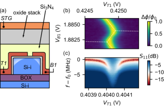
In this section, we show data obtained using our resonator with a different NWFET device. We exchange the device measured in the main section of the paper for one with a metal super-top gate (STG) which fully covers the poly-Si split gates, as shown in Fig. A9(a). The super-top gate is separated from the split-gates by 30 nm of Si3N4 followed by a 350 nm oxide stack. The nanowire and gate dimensions are the same as the previous device, but the devices are on different chips. The cavity resonance decreases slightly to GHz, which may be caused by a combination of the larger area of this silicon chip, and a small increase in the bond wire length. We tune the voltages of the three gates to the ICT shown in Fig. A9(b), where we estimate the total electron occupancy of the DQD to be around 20, similar to the dispersive regime in the previous device. We observe a large dispersive shift of 3.6 MHz in the cavity frequency, shown in Fig. A9(c), similar to the shift observed in Fig. 2(c) with the previous device. These results demonstrate the reproducibility of our approach across different devices.
Appendix F Condition of maximum state visibility for singlet-triplet readout
In order to calculate the condition of maximum state visibility, we calculate the maximum change in reflection coefficient between a singlet outcome, which induces a frequency shift , and triplet outcome that does not shift the resonator frequency Mizuta et al. (2017). Using Eq. 2, we find:
| (6) | ||||
We calculate the change in reflection coefficient and find:
| (7) |
The first condition for maximum state visibility occurs when Re. This requirement set the optimal operation detuning from the bare cavity frequency at , i.e. at the average frequency between singlet and triplet outcomes. In this case,
| (8) |
Equation 8 is maximum when , the condition of maximum state visibility. At this point , where is the coupling coefficient. Finally, we calculate the signal-to-noise ratio, knowing that photons leak out of the resonator at a rate
| (9) |
where is the photon noise and is the number of photons in the resonator. At the condition for maximum state visibility, for a critically coupled resonator driven at the critical photon number , we find
| (10) |
References
- Zwanenburg et al. (2013) Floris A. Zwanenburg, Andrew S. Dzurak, Andrea Morello, Michelle Y. Simmons, Lloyd C. L. Hollenberg, Gerhard Klimeck, Sven Rogge, Susan N. Coppersmith, and Mark A. Eriksson, “Silicon quantum electronics,” Rev. Mod. Phys. 85, 961–1019 (2013).
- Yoneda et al. (2018) Jun Yoneda, Kenta Takeda, Tomohiro Otsuka, Takashi Nakajima, Matthieu R Delbecq, Giles Allison, Takumu Honda, Tetsuo Kodera, Shunri Oda, Yusuke Hoshi, et al., “A quantum-dot spin qubit with coherence limited by charge noise and fidelity higher than 99.9%,” Nature nanotechnology 13, 102–106 (2018).
- Yang et al. (2019) C. H. Yang, K. W. Chan, R. Harper, W. Huang, T. Evans, J. C. C. Hwang, B. Hensen, A. Laucht, T. Tanttu, F. E. Hudson, S. T. Flammia, K. M. Itoh, A. Morello, S. D. Bartlett, and A. S. Dzurak, “Silicon qubit fidelities approaching incoherent noise limits via pulse engineering,” Nature Electronics 2, 151–158 (2019).
- Huang et al. (2019) W. Huang, C. H. Yang, K. W. Chan, T. Tanttu, B. Hensen, R. C. C. Leon, M. A. Fogarty, J. C. C. Hwang, F. E. Hudson, K. M. Itoh, A. Morello, A. Laucht, and A. S. Dzurak, “Fidelity benchmarks for two-qubit gates in silicon,” Nature 569, 532–536 (2019).
- Xue et al. (2019) X. Xue, T. F. Watson, J. Helsen, D. R. Ward, D. E. Savage, M. G. Lagally, S. N. Coppersmith, M. A. Eriksson, S. Wehner, and L. M. K. Vandersypen, “Benchmarking gate fidelities in a two-qubit device,” Phys. Rev. X 9, 021011 (2019).
- Zajac et al. (2018) David M Zajac, Anthony J Sigillito, Maximilian Russ, Felix Borjans, Jacob M Taylor, Guido Burkard, and Jason R Petta, “Resonantly driven cnot gate for electron spins,” Science 359, 439–442 (2018).
- Hutin et al. (2018) Louis Hutin, B Bertrand, Romain Maurand, A Crippa, M Urdampilleta, YJ Kim, A Amisse, H Bohuslavskyi, L Bourdet, Sylvain Barraud, et al., “Si mos technology for spin-based quantum computing,” in 2018 48th European Solid-State Device Research Conference (ESSDERC) (IEEE, 2018) pp. 12–17.
- Pillarisetty et al. (2019) R Pillarisetty, HC George, TF Watson, L Lampert, N Thomas, S Bojarski, P Amin, R Caudillo, E Henry, N Kashani, et al., “High volume electrical characterization of semiconductor qubits,” in 2019 IEEE International Electron Devices Meeting (IEDM) (IEEE, 2019) pp. 31–5.
- Zwerver et al. (2021) AMJ Zwerver, T Krähenmann, TF Watson, L Lampert, HC George, R Pillarisetty, SA Bojarski, P Amin, SV Amitonov, JM Boter, et al., “Qubits made by advanced semiconductor manufacturing,” arXiv preprint arXiv:2101.12650 (2021).
- Schaal et al. (2019) Simon Schaal, Alessandro Rossi, Virginia N Ciriano-Tejel, Tsung-Yeh Yang, Sylvain Barraud, John J L Morton, and M Fernando Gonzalez-Zalba, “A cmos dynamic random access architecture for radio-frequency readout of quantum devices,” Nature Electronics 2, 236–242 (2019).
- Fowler et al. (2012) Austin G. Fowler, Matteo Mariantoni, John M. Martinis, and Andrew N. Cleland, “Surface codes: Towards practical large-scale quantum computation,” Phys. Rev. A 86, 032324 (2012).
- Veldhorst et al. (2014) M Veldhorst, JCC Hwang, CH Yang, AW Leenstra, Bob de Ronde, JP Dehollain, JT Muhonen, FE Hudson, Kohei M Itoh, A Morello, et al., “An addressable quantum dot qubit with fault-tolerant control-fidelity,” Nature Nanotechnology 9, 981–985 (2014).
- Curry et al. (2019) M. J. Curry, M. Rudolph, T. D. England, A. M. Mounce, R. M. Jock, C. Bureau-Oxton, P. Harvey-Collard, P. A. Sharma, J. M. Anderson, D. M. Campbell, J. R. Wendt, D. R. Ward, S. M. Carr, M. P. Lilly, and M. S. Carroll, “Single-shot readout performance of two heterojunction-bipolar-transistor amplification circuits at millikelvin temperatures,” Scientific Reports 9, 16976 (2019).
- Urdampilleta et al. (2019) Matias Urdampilleta, David J. Niegemann, Emmanuel Chanrion, Baptiste Jadot, Cameron Spence, Pierre-André Mortemousque, Christopher Bäuerle, Louis Hutin, Benoit Bertrand, Sylvain Barraud, Romain Maurand, Marc Sanquer, Xavier Jehl, Silvano De Franceschi, Maud Vinet, and Tristan Meunier, “Gate-based high fidelity spin readout in a cmos device,” Nature Nanotechnology 14, 737–741 (2019).
- Volk et al. (2019) Christian Volk, Anasua Chatterjee, Fabio Ansaloni, Charles M Marcus, and Ferdinand Kuemmeth, “Fast charge sensing of si/sige quantum dots via a high-frequency accumulation gate,” Nano letters 19, 5628–5633 (2019).
- Keith et al. (2019) D. Keith, M. G. House, M. B. Donnelly, T. F. Watson, B. Weber, and M. Y. Simmons, “Single-shot spin readout in semiconductors near the shot-noise sensitivity limit,” Phys. Rev. X 9, 041003 (2019).
- Blais et al. (2004a) Alexandre Blais, Ren-Shou Huang, Andreas Wallraff, S. M. Girvin, and R. J. Schoelkopf, “Cavity quantum electrodynamics for superconducting electrical circuits: An architecture for quantum computation,” Phys. Rev. A 69, 062320 (2004a).
- Wallraff et al. (2004) Andreas Wallraff, David I Schuster, Alexandre Blais, Luigi Frunzio, R-S Huang, Johannes Majer, Sameer Kumar, Steven M Girvin, and Robert J Schoelkopf, “Strong coupling of a single photon to a superconducting qubit using circuit quantum electrodynamics,” Nature 431, 162–167 (2004).
- Blais et al. (2020) Alexandre Blais, Arne L Grimsmo, SM Girvin, and Andreas Wallraff, “Circuit quantum electrodynamics,” arXiv preprint arXiv:2005.12667 (2020).
- West et al. (2019) Anderson West, Bas Hensen, Alexis Jouan, Tuomo Tanttu, Chih-Hwan Yang, Alessandro Rossi, M Fernando Gonzalez-Zalba, Fay Hudson, Andrea Morello, David J Reilly, et al., “Gate-based single-shot readout of spins in silicon,” Nature nanotechnology 14, 437–441 (2019).
- Pakkiam et al. (2018) P. Pakkiam, A. V. Timofeev, M. G. House, M. R. Hogg, T. Kobayashi, M. Koch, S. Rogge, and M. Y. Simmons, “Single-shot single-gate rf spin readout in silicon,” Phys. Rev. X 8, 041032 (2018).
- Zheng et al. (2019) Guoji Zheng, Nodar Samkharadze, Marc L Noordam, Nima Kalhor, Delphine Brousse, Amir Sammak, Giordano Scappucci, and Lieven MK Vandersypen, “Rapid gate-based spin read-out in silicon using an on-chip resonator,” Nature nanotechnology 14, 742–746 (2019).
- Samkharadze et al. (2018) Nodar Samkharadze, Guoji Zheng, Nima Kalhor, Delphine Brousse, Amir Sammak, UC Mendes, Alexandre Blais, Giordano Scappucci, and LMK Vandersypen, “Strong spin-photon coupling in silicon,” Science 359, 1123–1127 (2018).
- Stockklauser et al. (2017) Anna Stockklauser, Pasquale Scarlino, J. V. Koski, Simone Gasparinetti, C. K. Andersen, Christian Reichl, Werner Wegscheider, Thomas Ihn, Klaus Ensslin, and Andreas Wallraff, “Strong coupling cavity qed with gate-defined double quantum dots enabled by a high impedance resonator,” Physical Review X 7, 011030 (2017).
- Veldhorst et al. (2017) M. Veldhorst, H. G. J. Eenink, C. H. Yang, and A. S. Dzurak, “Silicon cmos architecture for a spin-based quantum computer,” Nature Communications 8, 1766 (2017).
- Li et al. (2018) Ruoyu Li, Luca Petit, David P. Franke, Juan Pablo Dehollain, Jonas Helsen, Mark Steudtner, Nicole K. Thomas, Zachary R. Yoscovits, Kanwal J. Singh, Stephanie Wehner, Lieven M. K. Vandersypen, James S. Clarke, and Menno Veldhorst, “A crossbar network for silicon quantum dot qubits,” Science Advances 4, eaar3960 (2018).
- Schuster (2007) David Isaac Schuster, Circuit Quantum Electrodynamics, Ph.D. thesis, Department of Physics, Yale University, New Haven (2007).
- Ciriano-Tejel et al. (2021) Virginia N Ciriano-Tejel, Michael A Fogarty, Simon Schaal, Louis Hutin, Benoit Bertrand, M Fernando Gonzalez-Zalba, Jing Li, Y-M Niquet, Maud Vinet, and John JL Morton, “Spin readout of a cmos quantum dot by gate reflectometry and spin-dependent tunnelling,” PRX Quantum 2, 010353 (2021).
- Mi et al. (2018) Xiao Mi, Mónica Benito, Stefan Putz, David M Zajac, Jacob M Taylor, Guido Burkard, and Jason R Petta, “A coherent spin–photon interface in silicon,” Nature 555, 599–603 (2018).
- de Jong et al. (2019) Damaz de Jong, Jasper Van Veen, Luca Binci, Amrita Singh, Peter Krogstrup, L. P. Kouwenhoven, Wolfgang Pfaff, and J. D. Watson, “Rapid detection of coherent tunneling in an inas nanowire quantum dot through dispersive gate sensing,” Physical Review Applied 11, 044061 (2019).
- Sabonis et al. (2019) Deividas Sabonis, Eoin CT O’Farrell, Davydas Razmadze, David MT van Zanten, Judith Suter, Peter Krogstrup, and Charles M Marcus, “Dispersive sensing in hybrid inas/al nanowires,” Applied Physics Letters 115, 102601 (2019).
- Lundberg et al. (2020) Theodor Lundberg, Jing Li, Louis Hutin, Benoit Bertrand, David J Ibberson, Chang-Min Lee, David J Niegemann, Matias Urdampilleta, Nadia Stelmashenko, Tristan Meunier, et al., “A spin quintet in a silicon double quantum dot: Spin blockade and relaxation,” Phys. Rev. X 10, 041010 (2020).
- Betz et al. (2015) AC Betz, Romain Wacquez, Maud Vinet, Xavier Jehl, AL Saraiva, M Sanquer, AJ Ferguson, and MF Gonzalez-Zalba, “Dispersively detected pauli spin-blockade in a silicon nanowire field-effect transistor,” Nano letters 15, 4622–4627 (2015).
- Wisbey et al. (2010) David S Wisbey, Jiansong Gao, Michael R Vissers, Fabio CS da Silva, Jeffrey S Kline, Leila Vale, and David P Pappas, “Effect of metal/substrate interfaces on radio-frequency loss in superconducting coplanar waveguides,” Journal of Applied Physics 108, 093918 (2010).
- Khalil et al. (2012) MS Khalil, MJA Stoutimore, FC Wellstood, and KD Osborn, “An analysis method for asymmetric resonator transmission applied to superconducting devices,” Journal of Applied Physics 111, 054510 (2012).
- Ahmed et al. (2018) Imtiaz Ahmed, J. A. Haigh, Simon Schaal, Sylvain Barraud, Yi Zhu, Chang-min Lee, Mario Amado, J. W. A. Robinson, Alessandro Rossi, J. J. L. Morton, and M. F. Gonzalez-Zalba, “Radio-frequency capacitive gate-based sensing,” Physical Review Applied 10, 014018 (2018).
- Ibberson et al. (2019) David J Ibberson, Lisa A Ibberson, Geoff Smithson, James A Haigh, Sylvain Barraud, and M Fernando Gonzalez-Zalba, “Low-temperature tunable radio-frequency resonator for sensitive dispersive readout of nanoelectronic devices,” Applied Physics Letters 114, 123501 (2019).
- Mizuta et al. (2017) R. Mizuta, R. M. Otxoa, A. C. Betz, and M. F. Gonzalez-Zalba, “Quantum and tunneling capacitance in charge and spin qubits,” Physical Review B 95, 045414 (2017).
- Benito et al. (2017) Monica Benito, Xiao Mi, Jacob M Taylor, Jason R Petta, and Guido Burkard, “Input-output theory for spin-photon coupling in si double quantum dots,” Physical Review B 96, 235434 (2017).
- Gilbert et al. (2020) Will Gilbert, Andre Saraiva, Wee Han Lim, Chih Hwan Yang, Arne Laucht, Benoit Bertrand, Nils Rambal, Louis Hutin, Christopher C Escott, Maud Vinet, et al., “Single-electron operation of a silicon-cmos 2x2 quantum dot array with integrated charge sensing,” Nano Letters 20, 7882–7888 (2020).
- Yang et al. (2013) CH Yang, A Rossi, R Ruskov, NS Lai, FA Mohiyaddin, S Lee, C Tahan, Gerhard Klimeck, A Morello, and AS Dzurak, “Spin-valley lifetimes in a silicon quantum dot with tunable valley splitting,” Nature communications 4, 2069 (2013).
- Childress et al. (2004) L Childress, AS Sørensen, and Mikhail D Lukin, “Mesoscopic cavity quantum electrodynamics with quantum dots,” Physical Review A 69, 042302 (2004).
- Petersson et al. (2012) Karl D Petersson, Louis W McFaul, Michael D Schroer, Minkyung Jung, Jacob M Taylor, Andrew A Houck, and Jason R Petta, “Circuit quantum electrodynamics with a spin qubit,” Nature 490, 380–383 (2012).
- Dupont-Ferrier et al. (2013) E. Dupont-Ferrier, B. Roche, B. Voisin, X. Jehl, R. Wacquez, M. Vinet, M. Sanquer, and S. De Franceschi, “Coherent coupling of two dopants in a silicon nanowire probed by landau-zener-stückelberg interferometry,” Physical Review Letters 110, 136802 (2013).
- Gonzalez-Zalba et al. (2016) M Fernando Gonzalez-Zalba, Sergey N Shevchenko, Sylvain Barraud, J Robert Johansson, Andrew J Ferguson, Franco Nori, and Andreas C Betz, “Gate-sensing coherent charge oscillations in a silicon field-effect transistor,” Nano letters 16, 1614–1619 (2016).
- Chatterjee et al. (2018) Anasua Chatterjee, S. N. Shevchenko, Sylvain Barraud, R. M. Otxoa, Franco Nori, J. J. L. Morton, and M. F. Gonzalez-Zalba, “A silicon-based single-electron interferometer coupled to a fermionic sea,” Physical Review B 97, 045405 (2018).
- Blais et al. (2004b) Alexandre Blais, Ren-Shou Huang, Andreas Wallraff, S. M. Girvin, and R. J. Schoelkopf, “Cavity quantum electrodynamics for superconducting electrical circuits: An architecture for quantum computation,” Physical Review A 69, 062320 (2004b).
- Yan et al. (2016) Fei Yan, Simon Gustavsson, Archana Kamal, Jeffrey Birenbaum, Adam P Sears, David Hover, Ted J Gudmundsen, Danna Rosenberg, Gabriel Samach, Steven Weber, et al., “The flux qubit revisited to enhance coherence and reproducibility,” Nature communications 7, 12964 (2016).
- Maman et al. (2020) Vahid Derakhshan Maman, M. F. Gonzalez-Zalba, and András Pályi, “Charge noise and overdrive errors in reflectometry-based charge, spin and majorana qubit readout,” Phys. Rev. Applied 14, 064024 (2020).
- Schaal et al. (2020) S. Schaal, I. Ahmed, J. A. Haigh, L. Hutin, B. Bertrand, S. Barraud, .M Vinet, C-M Lee, N. Stelmashenko, J. W. A. Robinson, J. Y. Qiu, S. Hacohen-Gourgy, I. Siddiqi, M. F. Gonzalez-Zalba, and J. J. L. Morton, “Fast gate-based readout of silicon quantum dots using josephson parametric amplification,” Physical Review Letters 124, 067701 (2020).
- Stehlik et al. (2015) J. Stehlik, Y-Y Liu, C. M. Quintana, C. Eichler, T. R. Hartke, and J. R. Petta, “Fast charge sensing of a cavity-coupled double quantum dot using a josephson parametric amplifier,” Physical Review Applied 4, 014018 (2015).
- Barthel et al. (2009) Christian Barthel, D. J. Reilly, C. M. Marcus, M. P. Hanson, and A. C. Gossard, “Rapid single-shot measurement of a singlet-triplet qubit,” Physical Review Letters 103, 160503 (2009).
- Hornibrook et al. (2014) JM Hornibrook, JI Colless, AC Mahoney, XG Croot, S Blanvillain, H Lu, AC Gossard, and DJ Reilly, “Frequency multiplexing for readout of spin qubits,” Applied Physics Letters 104, 103108 (2014).
- Heinsoo et al. (2018) Johannes Heinsoo, C. K. Andersen, Ants Remm, Sebastian Krinner, Theodore Walter, Yves Salathé, Simone Gasparinetti, Jean-Claude Besse, Anton Potočnik, Andreas Wallraff, and Christopher Eichler, “Rapid high-fidelity multiplexed readout of superconducting qubits,” Physical Review Applied 10, 034040 (2018).
- Koch et al. (2007) Jens Koch, T. M. Yu, Jay Gambetta, A. A. Houck, D. I. Schuster, J Majer, Alexandre Blais, M. H. Devoret, S. M. Girvin, and R. J. Schoelkopf, “Charge-insensitive qubit design derived from the cooper pair box,” Physical Review A 76, 042319 (2007).
- Boross et al. (2016) Péter Boross, Gábor Széchenyi, and András Pályi, “Valley-enhanced fast relaxation of gate-controlled donor qubits in silicon,” Nanotechnology 27, 314002 (2016).
- Mi et al. (2017) Xiao Mi, JV Cady, DM Zajac, PW Deelman, and Jason R Petta, “Strong coupling of a single electron in silicon to a microwave photon,” Science 355, 156–158 (2017).
- Scarlino et al. (2019) Pasquale Scarlino, D. J. van Woerkom, Anna Stockklauser, J. V. Koski, M. C. Collodo, Simone Gasparinetti, Christian Reichl, Werner Wegscheider, Thomas Ihn, Klaus Ensslin, and Andreas Wallraff, “All-microwave control and dispersive readout of gate-defined quantum dot qubits in circuit quantum electrodynamics,” Physical Review Letters 122, 206802 (2019).
- Crippa et al. (2019) A Crippa, R Ezzouch, A Aprá, A Amisse, R Laviéville, L Hutin, B Bertrand, M Vinet, M Urdampilleta, T Meunier, et al., “Gate-reflectometry dispersive readout and coherent control of a spin qubit in silicon,” Nature communications 10, 1–6 (2019).
- Maurand et al. (2016) R Maurand, X Jehl, D Kotekar-Patil, A Corna, H Bohuslavskyi, R Laviéville, L Hutin, S Barraud, M Vinet, M Sanquer, et al., “A cmos silicon spin qubit,” Nature communications 7, 1–6 (2016).
- Forn-Díaz et al. (2019) P. Forn-Díaz, L. Lamata, E. Rico, J. Kono, and E. Solano, “Ultrastrong coupling regimes of light-matter interaction,” Reviews of Modern Physics 91, 025005 (2019).
- Khalil et al. (2010) Moe S Khalil, F. C. Wellstood, and Kevin D Osborn, “Loss dependence on geometry and applied power in superconducting coplanar resonators,” IEEE Transactions on Applied Superconductivity 21, 879–882 (2010).
- Sage et al. (2011) Jeremy M Sage, Vladimir Bolkhovsky, William D Oliver, Benjamin Turek, and Paul B Welander, “Study of loss in superconducting coplanar waveguide resonators,” Journal of Applied Physics 109, 063915 (2011).
- Hayashi et al. (2014) K Hayashi, A Saito, Y Ogawa, M Murata, T Sawada, K Nakajima, H Yamada, S Ariyoshi, T Taino, H Tanoue, et al., “Design and fabrication of microwave kinetic inductance detectors using nbn symmetric spiral resonator array,” in Journal of Physics: Conference Series, Vol. 507 (IOP Publishing, 2014) p. 042015.
- Peruzzo et al. (2020) M. Peruzzo, A. Trioni, F. Hassani, M. Zemlicka, and J. M. Fink, “Surpassing the resistance quantum with a geometric superinductor,” Physical Review Applied 14, 044055 (2020).
- Jerger et al. (2012) Markus Jerger, Stefano Poletto, Pascal Macha, Uwe Hübner, Evgeni Il’ichev, and Alexey V Ustinov, “Frequency division multiplexing readout and simultaneous manipulation of an array of flux qubits,” Applied Physics Letters 101, 042604 (2012).