Layout and Performance of HPK Prototype LGAD Sensors for the High-Granularity Timing Detector
Abstract
The High-Granularity Timing Detector is a detector proposed for the ATLAS Phase II upgrade. The detector, based on the Low-Gain Avalanche Detector (LGAD) technology will cover the pseudo-rapidity region of with two end caps on each side and a total area of . The timing performance can be improved by implanting an internal gain layer that can produce signal with a fast rising edge, which improve significantly the signal-to-noise ratio. The required average timing resolution per track for a minimum-ionising particle is at the start and at the end of the HL-LHC operation. This is achieved with several layers of LGAD. The innermost region of the detector would accumulate a -neutron equivalent fluence up to before being replaced during the scheduled shutdowns. The addition of this new detector is expected to play an important role in the mitigation of high pile-up at the HL-LHC. The layout and performance of the various versions of LGAD prototypes produced by Hamamatsu (HPK) have been studied by the ATLAS Collaboration. The breakdown voltages, depletion voltages, inter-pad gaps, collected charge as well as the time resolution have been measured and the production yield of large size sensors has been evaluated.
keywords:
Low-Gain Avalanche Detector , HGTD , Timing Detector1 Introduction
Low-Gain Avalanche Detectors (LGAD) [1] have become one of the most precise detector technologies for timing measurements due to their internal gain mechanism. It was proposed by the RD50 collaboration and developing by CNM [2], FBK [3], BNL [4] and HPK [5]. Recent developments concentrate on the optimization of the pad periphery and the doping profile to prevent premature breakdown and maintain the performance of the sensor after extremely high fluences of hadron irradiation. After several years of research, the properties of LGADs have become better known. In order to apply the technology in the ATLAS HGTD upgrade [6], the sensors need to maintain a time resolution per hit better than after -neutron equivalent fluence. HPK has produced the first batch of wafers of LGADs to HGTD specifications and these sensors have been tested by the ATLAS HGTD sensor group with methods including I-V (Current-voltage) curves, C-V (Capacitance–voltage) profiling, TCT (Transient Current Technique) [7], beta scope [8], and several test beams [9]. The performances of these sensors before irradiation are shown in this paper.
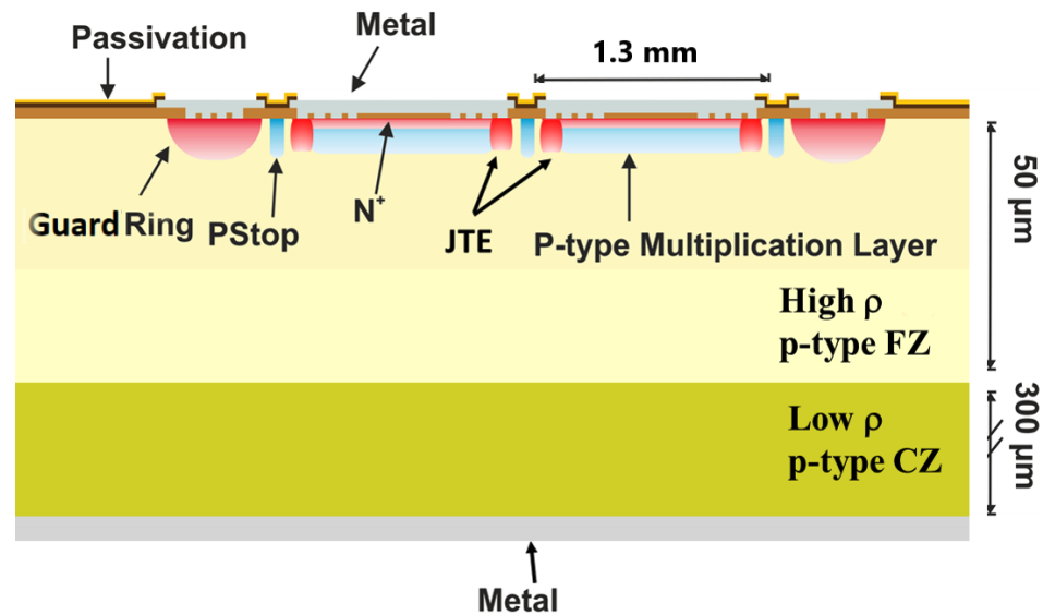
With a common mask, sensors with an active thickness of (HPK-1.1-35, HPK-1.2-35 and HPK-2-35) and (HPK-3.1-50 and HPK-3.2-50) were produced by HPK. The different types refer to different combinations of doping profile of the gain layer and resistivity of the bulk. The cross section of a sensor with a array of pads is shown in Figure 1. The layout of the arrays is based on the pad size.
Single pads with different distances to the edge and arrays with different inter-pad (IP) gap were fabricated to determine a safe separation between pads. Large arrays with and pads were produced and studied for the first time to demonstrate the feasibility of large sensors and to investigate the yield, for which the sensors are tested and classified in terms of breakdown voltages. The layouts of the HPK sensors are presented in Table 1. The dynamic properties are measured with charged particles or infrared laser. The collected charge and time resolutions are measured at different voltages.
LGADs with active thickness have higher capacitance, smaller generated charge and larger power dissipation after irradiation than those with active thickness [11]. Hence, it has been decided that sensors will not be used for the HGTD project. The detailed studies including IP gap, yield and uniformity only focus on the HPK-3.1-50 and HPK-3.2-50 sensors.
| Size | Edge [] | Nominal IP Gap [] | Total # per wafer |
| Single | 200,300,500 | - | 132 |
| arrays | 200,300,500 | 30,50,70,95 | 70 |
| arrays | 300 | 95 | 4 |
| arrays | 500 | 95 | 18 |
| arrays | 500 | 95 | 8 |

2 Setup for I-V and C-V measurements
The I-V and C-V measurements are proceed under probe stations. The probe needles are used for sensors with single pad and pad array for which up to five needles are used to make the guard ring or neighbor pads grounded. For pad array, a dedicated probe card is designed to contact all 25 pads and guard ring simultaneously as shown in Figure 2. The channel under measurement is selected by a channel switch board while other channels remain grounded. The switch board could be controlled by computer via the USB connection so that a scan of total 25 pad could be performed semi-automatically. For pad array, the measurements are taking under a automatic probe station with the probe needle, the guard ring is grounded while other pads not measured remain floating. The probe card for sensors is under developing and would be applied in the future measurement.
The high reverse bias voltage (HV) is supplied by the metal chuck of the probe station. All sensors before irradiation are measured under room temperature (about ) and relative humidity around 20%-50% depending on the weather. The sensors are protected from light by the black shield box during the measurement.
For the I-V measurement, the sensor is connected with source measure unit (SMU) which can bias sensors up to around and measure the current at sub- level. The high precision current meter with precision is series connected to the channel under test when a high precision I-V is needed. The compliance current is set to several to avoid the potential damage to the instruments or sensors when breakdown. A time interval large than and a ramping speed lower than are assured at each bias point to ensure stability of the measurement circuit.
As for C-V measurement, besides the SMU to provide the HV, a LCR meter is connected in parallel by an HV adaptor [12] to measure the AC character of the device. Apart form the current compliance set in I-V, a ziener diode is connected with sensor in parallel to limit the voltage in a safe range for LCR. The ”Cp-Rp” working mode and a frequency is used for un-irradiated sensors as the recommendation of RD50 [13]. An AC amplitude of and a step of is used to measure the character of the gain layer. The step is further limited to near the depletion voltage to have the fine structure measured. In order to ensure stability, the capacitance is read out every , after the bias voltage is set, and is saved only when the relative difference with respect to the previous measurement is less than 0.1%.
3 I-V, uniformity and yield
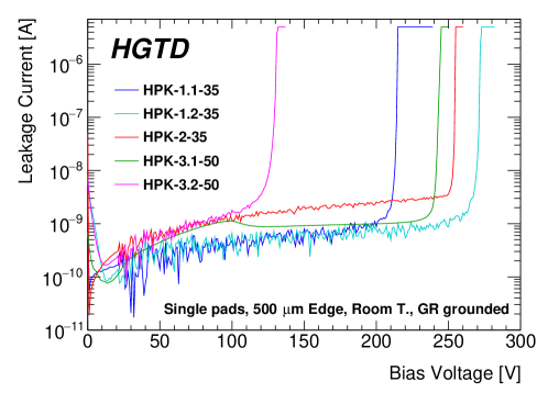
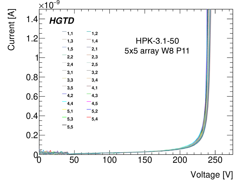
The I-V for each single pad sensor is measured at room temperature with single needle and the guard ring grounded. The results are shown in Figure 3. The distribution of leakage current and breakdown voltage on HPK-3.1-50 single pad sensors are shown in Figure 4(a) and (b). In Figure 4(c), the I-V curves of each pad on an HPK-3.1-50 sensor measured with a probe card show a good uniformity. The breakdown voltage () is defined with these curves by the bias voltage corresponding to a leakage current of .
The performances of different types of sensors are compared on single pads with exactly the same geometry. For the sensors, the HPK-1.1-35 sensors have breakdown voltages of , while type HPK-1.2-35 with the similar gain layer implantation as type HPK-1.1-35 but a higher bulk resistivity shows a higher breakdown voltage of . The HPK-2-35 sensor which has the similar bulk resistivity as HPK-1.1-35 but shallower and wider doping shows a higher breakdown voltage of . For the sensors, the major difference between HPK-3.1-50 and HPK-3.2-50 is the depth of the gain layer implantation. For HPK-3.1-50 which has a shallower implantation, the breakdown voltage is . HPK-3.2-50 has a deeper implantation and its breakdown voltage is , which is much lower. All sensors are measured to have a low leakage current level (sub-) before breakdown.

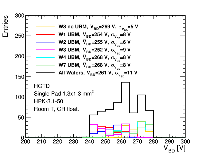
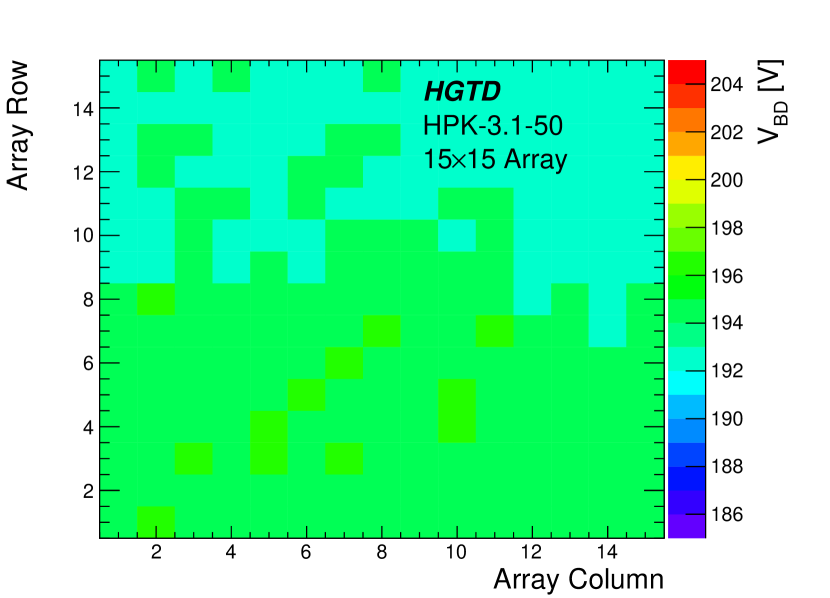
Since the HGTD needs a very large number of modules with arrays of LGADs, the large scale yield is important for the sensor fabrication. We have summarized the fraction of good pads and perfect sensors in different array size for the yield estimation (see Table 2). The good pads are defined as pads having a breakdown voltage above 90% of the nominal value and a perfect sensor is a sensor with 100% good pads in it. The fraction of perfect sensors is 100% for all sensors with single pad or , arrays of pads. For sensors with arrays of pads, the fraction of perfect sensors is 85.2% for HPK-3.1-50, 91.3% for HPK-3.2-50 and the fraction of good pads is 99.5% for HPK-3.1-50, 99.8% for HPK-3.2-50.
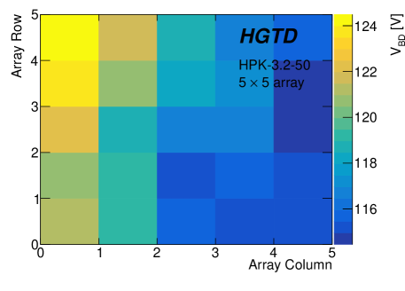
The uniformity of the pads in large arrays is also important. For all HPK-3.1-50 wafers evaluated, the uniformity has been shown by the distributions of leakage current, breakdown voltage and the breakdown voltage of all pads in a array in Figure 4. The distribution of breakdown voltage on an HPK-3.2-50 array is shown in Figure 5. An acceptable uniformity has been observed. It is also observed that the breakdown voltages of arrays are slightly lower than those of single pad sensors, most likely due to the differences in surrounding structures.
![[Uncaptioned image]](/html/2003.14071/assets/x7.png)
4 C-V and depletion voltage
4.1 Single pad C-V of each type
To estimate the voltage required to deplete the gain layer () and the bias to deplete the bulk (), C-V curves of each type’s single pads are measured with probe needle and shown in Figure 6(a).
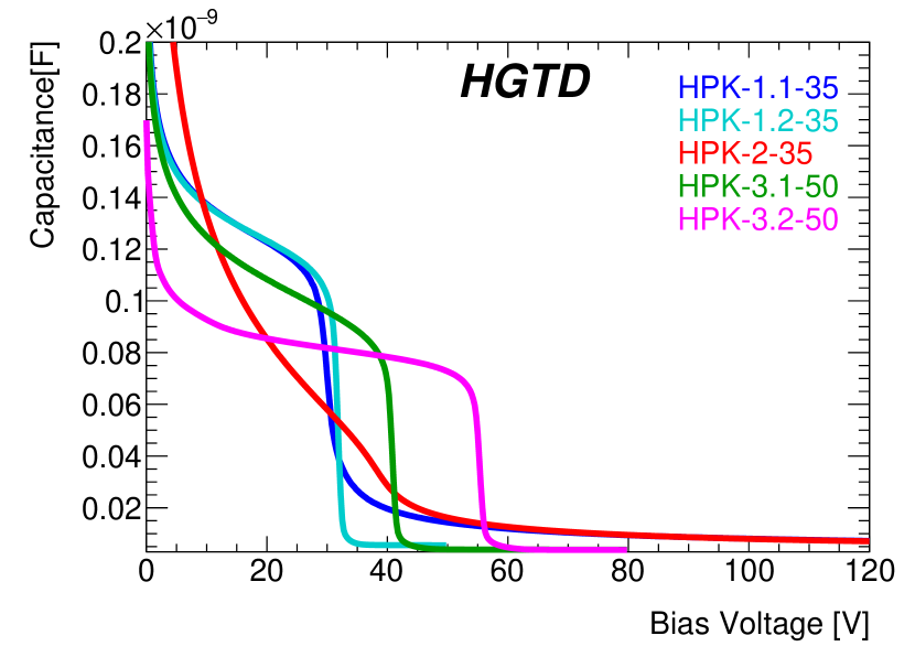
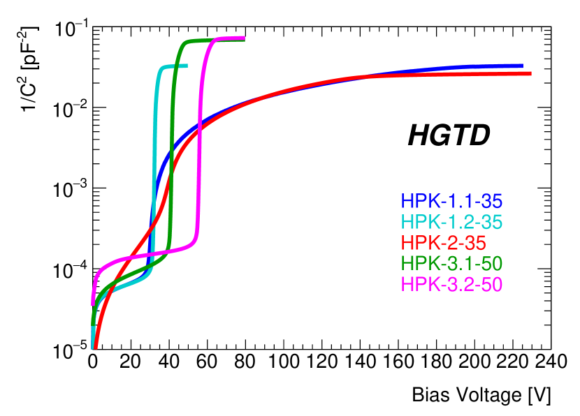
For a typical p-n junction, the behavior of -V curve is closely related to the distribution of dopants [15]. It can be used to study the multiplication layer of the LGAD. Several parameters from -V curves in Figure 6(b) are determined to compare the sensors. For each type of the sensor, the is estimated by finding the voltage where the -V curves start rising [16], and the is the voltage where the curves saturate. The precise turning points are determined by extrapolating from the adjacent segments before and after the transition region and finding the intersections of the extrapolations. The gain layer depletion voltage is about to for HPK-1.1-35 and HPK-1.2-35, to for HPK-2-35 and HPK-3.1-50 and for HPK-3.2-50.
After gain layer depletion, the -V curves of HPK-1.2-35, HPK-3.1-50 and HPK-3.2-50 sensors rise much faster than other types and become flat at relatively low voltage, indicating a higher resistivity in the bulk. The full depletion voltages for HPK-1.2-35, HPK-3.1-50 and HPK-3.2-50 sensors are estimated to be in the range of 40-, and those for HPK-1.1-35, HPK-2-35 are above , indicting a lower resistive bulk. Detailed depletion voltages obtained from C-V are summarized in Table 3.
| Type | [] | [] |
|---|---|---|
| HPK-1.1-35 | 31 | 195 |
| HPK-1.2-35 | 33 | 36 |
| HPK-2-35 | 40 | 144 |
| HPK-3.1-50 | 42 | 49 |
| HPK-3.2-50 | 56 | 64 |
4.2 Uniformity study of the gain layer
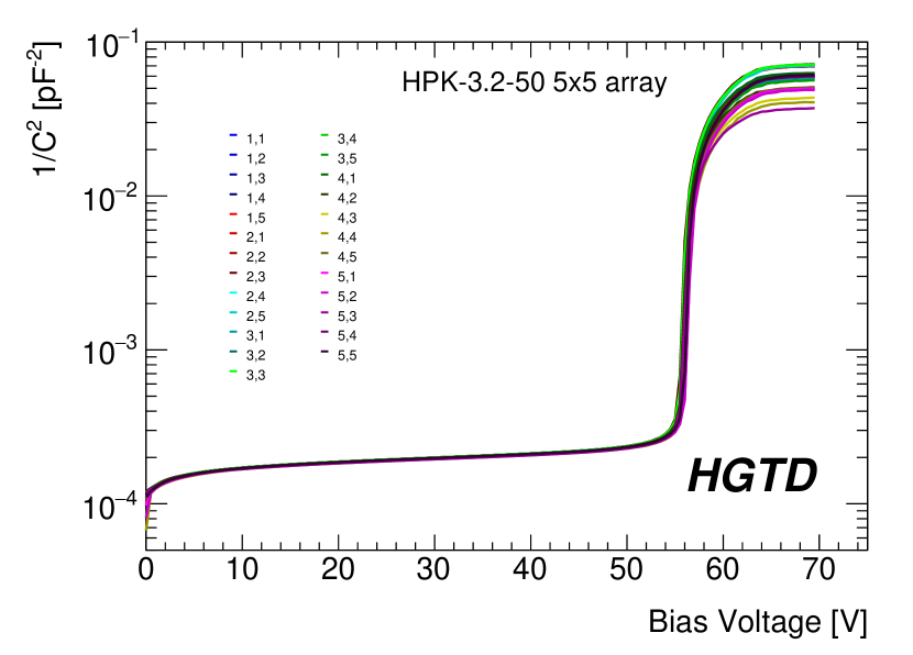
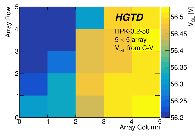
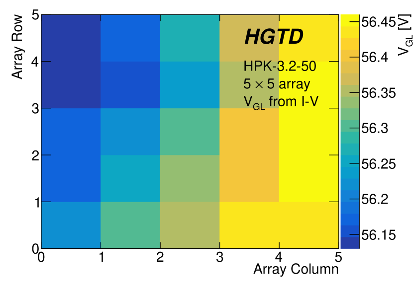
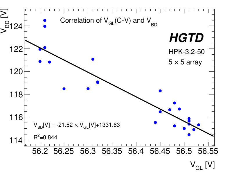
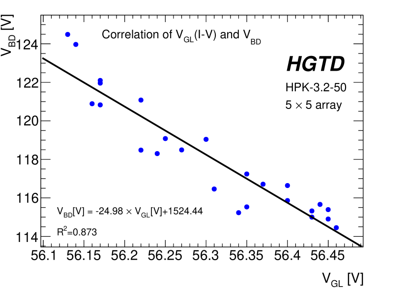
Since the front-end chip used to used to read out the sensor provides a common ground to the sensor and the bias voltage is common to a full pad array simultaneously, the uniformity of gain layer should be well controlled. Due to the fact that a small variation on boron implantation dose would result in a large variation on as shown in Figure 5. Assuming a fixed acceptor distribution, the total boron implantation dose should be proportional to the . Thus a measurement of variation is important. The resistance of a biased sensor is dependent on the depth of the depletion zone [2]. Thus I-V curves (Figure 7(a)) can also be used to estimate besides the C-V curves (Figure 7(b)). Here, the I-V curves of a array are measured with finer steps, slower HV ramping rate to derive the of each pad. Figure 8 (a) and (b) show the distribution of from I-V and C-V on a same HPK-3.2-50 array. The correlation between and is shown in Figure 8 (c) and (d). The mean value as well as variation are summarized in the Table 4. The results from both methods are close. Finally, a 0.2% variation on boron implantation dose is observed, which results in a 2.5% variation on .

| Method | from C-V | from I-V | |
|---|---|---|---|
| Mean value [V] | 56.38 | 56.31 | 118.12 |
| RMS/Mean 100% | 0.22% | 0.19% | 2.48% |
5 Inter-pad Gap
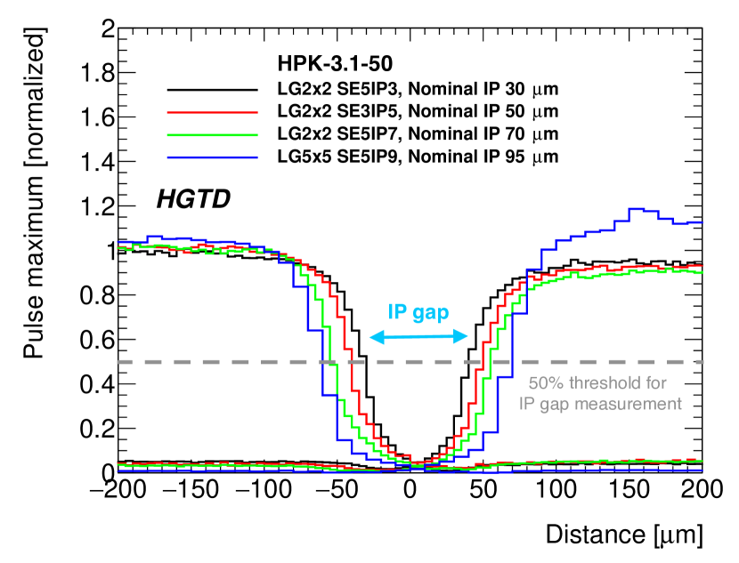
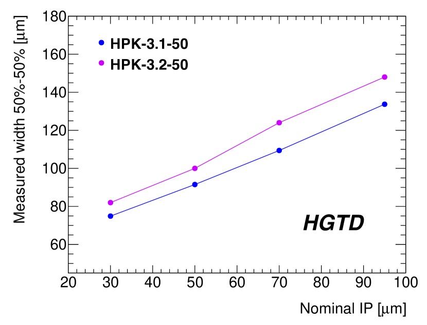
The infrared laser TCT is used for IP gap studies by scanning over the region between two adjacent pads. The nominal value of the IP gap is defined as the distance between the multiplication region of adjacent pads, which ranges from to for HPK LGAD arrays. Experimentally, the IP gap is here defined by the region between adjacent pads where the pulse height is below 50% of that in the central area of a pad. As shown in Figure 9, the measured IP gap is always about to larger than the nominal due to that the field lines under the multiplication area are bent towards the peripheral region where JTE (Junction Termination Extension) lies with no gain. This effect would be reduced by irradiation because of removed JTE doping and increased bulk gain. The IP gap of HPK-3.1-50 is always measured to be slightly lower than the one of HPK-3.2-50 and an IP gap of is achieved at the lowest nominal IP gap of , which corresponds to a fill factor around 90%.
6 Time resolution and collected charge
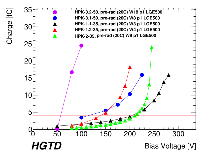
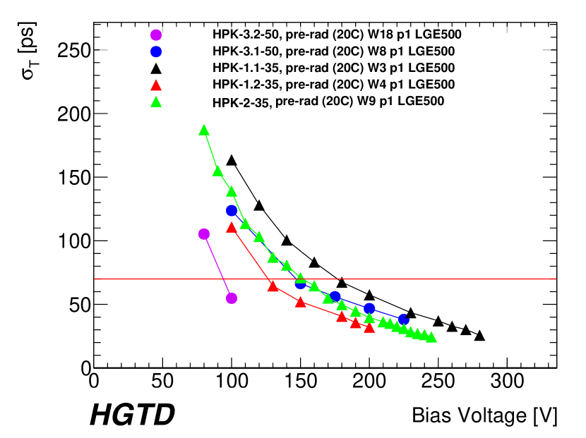
The collected charge as well as the time resolution at different bias voltages are measured with a -scope system [5]. The time resolution are extracted with a reference fast HPK LGAD with of time resolution which also acts as a trigger. The result are shown in Figure 10(a), from which we can see different performance resulting from different design. Due to high implantation and early breakdown, HPK-3.2-50 has to be operated at low bias, just after full depletion, and the carrier velocity is not saturated. This results in a reduced time resolution performance. The time resolution under different bias voltages are summarized in 10(b), which shows that all types except HPK-3.2-50 have reached the time resolution below before breakdown. The sensors are irradiated by proton from accelerators (CYRIC, Los Alamos) and neutrons from a reactor source (JSI), the performances after irradiation are summarized in another paper [11].
7 Conclusion
LGAD sensors produced by HPK have been studied extensively by the ATLAS HGTD group. The breakdown voltage and depletion voltage of each type have been characterized by I-V and C-V measurements to determine the window for detector operation. A measured effective inter-pad gap of has been achieved by HPK-3.1-50 sensors. The variation of is measured to characterize the fluctuation of gain layer implantation and a 0.2% variation is observed.
The fractions of good pads and perfect sensors are estimated for each array size. Good uniformities are observed in leakage currents and breakdown voltages and the feasibility of large size sensors production has been demonstrated. Time resolution and collected charges are measured by a -scope and time resolution below is achieved.
Acknowledgement
This work was supported by the United States Department of Energy, grant DE-FG02-04ER41286, “the Fundamental Research Funds for the Central Universities” of China (grant WK2030040100), the National Natural Science Foundation of China (No. 11961141014), the State Key Laboratory of Particle Detection and Electronics (SKLPDE-ZZ-202001), the Hundred Talent Program of the Chinese Academy of Sciences (Y6291150K2), the CAS Center for Excellence in Particle Physics (CCEPP), the MINECO, Spanish Government, under grant RTI2018-094906-B-C21, the Slovenian Research Agency (project J1-1699 and program P1-0135), the U.S.A. Department of Energy under grant contact DE-SC0012704 and partially carried out at the USTC Center for Micro and Nanoscale Research and Fabrication and partially performed within the CERN RD50 collaboration. The contributions from UCSC technical staff and students is acknowledged.
References
- [1] H.-W. Sadrozinski, A. Anker, J. C. et al., Ultra-fast silicon detectors (UFSD), Nucl. Instrum. Meth. A 831 (2016) 18 – 23, proceedings of the HSTD12. doi:https://doi.org/10.1016/j.nima.2016.03.093.
- [2] G. Pellegrini, P. Fernández-Martínez, M. Baselga et al., Technology developments and first measurements of Low Gain Avalanche Detectors (LGAD) for high energy physics applications, Nucl. Instrum. Meth. A 765 (2014) 12–16.
- [3] V. Sola, R. Arcidiacono, M. Boscardin et al., First FBK Production of 50um Ultra-Fast Silicon Detectors, Nucl. Instrum. Meth. A (02 2018). doi:10.1016/j.nima.2018.07.060.
- [4] G. Giacomini, W. Chen, F. Lanni et al., Development of a technology for the fabrication of Low-Gain Avalanche Diodes at BNL, Nucl. Instrum. Meth. A 934 (2019) 52–57.
- [5] Z. Galloway, V. Fadeyev, P. Freeman et al., Properties of HPK UFSD after neutron irradiation up to 6e15 n/cm2, Nucl. Instrum. Meth. A 940 (2019) 19 – 29. doi:10.1016/j.nima.2019.05.017.
-
[6]
ATLAS Collaboration, Technical
Proposal: A High-Granularity Timing Detector for the ATLAS Phase-II
Upgrade, Tech. Rep. CERN-LHCC-2018-023. LHCC-P-012, CERN, Geneva (Jun
2018).
URL https://cds.cern.ch/record/2623663 - [7] M. Schwickardi, Characterisation of Low Gain Avalanche Detectors, II.Physik-UniGö-MSc-2019/06, Master’s thesis, University of Göttingen (2019).
- [8] Y. Zhao, N. Cartiglia, E. E. et al., Comparison of 35 and 50um thin HPK UFSD after neutron irradiation up to 6e15 neq/cm2, Nucl. Instrum. Meth. A 924 (2019) 387 – 393, 11th International Hiroshima Symposium on Development and Application of Semiconductor Tracking Detectors. doi:10.1016/j.nima.2018.08.040.
- [9] C. Allaire, J. Benitez, M. Bomben et al., Beam test measurements of Low Gain Avalanche Detector single pads and arrays for the ATLAS High Granularity Timing Detector, Journal of Instrumentation 13 (06) (2018) P06017–P06017. doi:10.1088/1748-0221/13/06/p06017.
-
[10]
G. Pellegrini,
Status of
LGAD productions at CNM, 30th RD50 workshop (2017).
URL https://indico.cern.ch/event/637212/contributions/2608652/ -
[11]
X. Shi,
Radiation
Campaign of HPK Prototype LGAD sensors for the High-Granularity Timing
Detector, 12th International Hiroshima Symposium on Development and
Application of Semiconductor Tracking Detectors (2019).
URL https://indico.cern.ch/event/803258/contributions/3582870/ - [12] A. Technologies, Agilent Impedance measurement handbook (2009).
-
[13]
RD50 Collaboration.
URL http://rd50.web.cern.ch/rd50 -
[14]
ATLAS Collaboration,
HGTD
Public Plots, ATLAS Public Twiki (2019).
URL https://twiki.cern.ch/twiki/bin/view/AtlasPublic/LArHGTDPublicPlots - [15] L. Rossi, P. Fischer, T. Rohe, N. Wermes, Pixel detectors: From fundamentals to applications, Springer Science & Business Media, 2006.
-
[16]
H. Sadrozinski,
In-depth
experimental Study of Acceptor Removal in Low-Gain Avalanche Detectors, 12th
International Hiroshima Symposium on Development and Application of
Semiconductor Tracking Detectors (2019).
URL https://indico.cern.ch/event/803258/contributions/3582868/