Universal Model for Electron Thermal-Field Emission from
Two-Dimensional Semimetals
Abstract
We present the theory of out-of-plane (or vertical) electron thermal-field emission from 2D semimetals. We show that the current-voltage-temperature characteristic is well-captured by a universal scaling relation applicable for broad classes of 2D semimetals, including graphene and its few-layer, nodal point semimetal, Dirac semimetal at the verge of topological phase transition and nodal line semimetal. Here an important consequence of the universal emission behavior is revealed: in contrast to the common expectation that band topology shall manifest differently in the physical observables, band topologies in two spatial dimension are indistinguishable from each others and bear no special signature in the electron emission characteristics. Our findings represent the quantum extension of the universal semiclassical thermionic emission scaling law in 2D materials, and provide the theoretical foundations for the understanding of electron emission from cathode and charge interface transport for the design of 2D-material-based vacuum nanoelectronics.
I Introduction
Since the first field emission model or the well known Fowler-Nordheim (FN) law was formulated about a century ago FN , it remains an active topic to discover various materials as emitters, geometrical configuration, and different operating conditions for diode physics and high power microwaves PHP2008 ; p_zhang ; JAP2021 . It is expected that the traditional emission models are no longer valid for for quantum materials such as two-dimensional (2D) materials like graphene, transition-metal dichalcogenide (TMD) materials, and topological materials (like topological insulators and semimetals) IEEE2022 ; InfoMat2021 . In two-dimensional (2D) materials, the extreme confinement of electrons within atomic-scale thickness and the existence of unusual emergent fermions with exotic energy dispersions lead to the occurrence of unusual transport properties that are radically different from that of the three-dimensional bulk materials neto ; sangwan . Klein tunneling katsnelson , unconventional quantum Hall effect novoselov , quantum spin Hall insulating phase kane , valley contrasting transport d_xiao and spontaneous berryogenesis j_song are some of the most extraordinary transport phenomena discovered in 2D materials.
Compared to field emission, thermionic emission due to 2D materials have been studied more intensively ang3 ; ang1 ; PRAp2016 ; PRAp2015 ; trushin1 ; trushin2 In the case of thermionic emission where electrons are emitted from a solid surface via semiclassical thermal excitation pathway, the existence of a universal current-temperature scaling law represents another fascinating transport manifestations of the reduced dimensionality of 2D materials, where the universal temperature scaling laws were obtained ang1 , signifying the breakdown of the century-old Richardson-Dushman thermionic emission theory RD .
For field emission jensen_text , electron can undergo quantum mechanical tunneling due the narrowing of the interface potential barrier caused by an external applied electric field. For classical materials, the Fowler-Nordheim (FN) theory FN ; schottky provides the key theoretical foundation, and has formed one of the central pillars of vacuum electronics at the dawn of twentieth century. Remarkably, field emission physics remains highly important to solid-state devices in the post vacuum tube era because of its critical role in the interfacial charge injection process across the metal/insulator and metal/semiconductor interfaces sze which are omnipresent in modern electronic and optoelectronic devices. Due to its technological importance in both vacuum han and solid-state device technology, FN theory has been continually refined over the past decades MG ; burgess ; stratton ; forbes2 ; jensen ; kyritsakis ; sd_liang ; wei ; Steve ; Sim ; Sim2 .
For quantum 2D materials, the validity of FN based models need to be scrutinized since the foundational bases of such theories, particularly the assumption of 3D quasi-free electron gas with parabolic dispersion, are fundamentally incompatible with the physical properties of 2D material ang2 . Despite ongoing experimental eda ; qian ; wu ; xiao ; palnitka ; yamaguchi ; huang ; moussa ; wu_GVT ; wu_SFE ; xu ; bartolomeo ; rezaeifar ; q_ma and theoretical wei3 ; song ; wang ; d_jena efforts in unearthing the physics of electron emission from graphene, a comprehensive understanding of electron out-of-plane (or vertical) field emission from the broader family of 2D semimetals remains largely incomplete thus far. The following questions remain open: What is the radical difference(s) between the electron field emission in 2D and 3D materials? Is there a simple unifying scaling relation, counterpart to the universal current-temperature scaling law of semiclassical thermionic emission ang1 , that encompasses the field emission characteristics for broad classes of 2D semimetals? Recently, we have reported that the FN law is no longer valid for 3D Dirac and Weyl semi-metals PRB2021 . These non-FN field emission models will not converge to space charge limited current condition PRAp2021 .
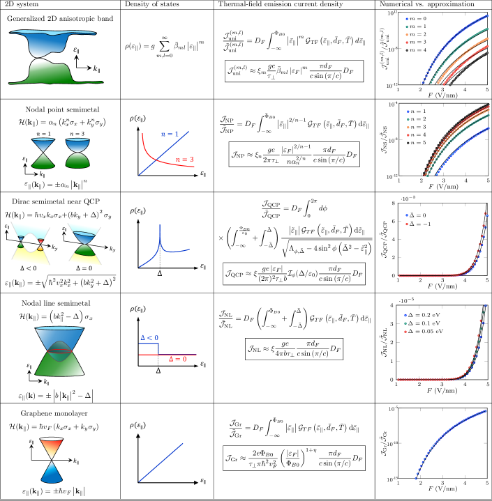
In this work, we will address the above questions by developing the theory of out-of-plane electron thermal-field emission from 2D semimetals. We present the full numerical and analytical approximate expressions of the thermal-field emission current MG for various 2D semimetals, including graphene and its few-layer neto , nodal point semimetals burkov of generalized pseudospin vorticity moore , Dirac semimetals at the verge of topological quantum phase transition roy and nodal line semimetals fang . Remarkably, by employing a generalized model of 2D semimetals ang1 , we show that the vertical emission current density () for broad classes of 2D semimetals can be accurately captured by a universal current-field-temperature scaling law,
| (1) |
where and are material-dependent parameters, is the electric field strength, is the emitter temperature, is a field-dependent parameter (defined below), and . A particularly intriguing feature of Eq. (1) is its departure from the bulk material thermal-field emission scaling relation of MG , thus revealing the breakdown of the classic FN-type electron emission model. Note this linear dependence of the field in the prefactor (for field emission) is similar to the pure thermionic emission reported ang1 .
The universal field emission scaling law identified here reveals an important fundamental feature of band topology in two spatial dimensions: in contrast to the common expectation that different band topologies shall manifest differently in the electronic, optical, electrical, mechanical and thermodynamical properties, as already demonstrated in the density of states j_wang , transport j_hu ; hp_sun , optical response tabert ; carbotte , quantum oscillations c_wang ; c_li , many-body physics roy2 ; sur , and shear viscosity moore , band topologies in two spatial dimensions are indistinguishable from each others and bears no special signatures in the electron emission current-field scaling characteristics. Nonetheless, the Fermi level dependence of the emission current does reflects the differences in the energy dispersion of various 2D semimetals. As electron field emission is a crucially important charge transport mechanism in both solid/vacuum p_zhang and solid/solid interfaces allain ; xu_rev , the model developed here shall offer a pivotal theoretical foundation for both the fundamental understanding of surface and nanoscale interface physics, and the practical design of high-performance vacuum zhou and solid-state devices based on 2D materials and their van der Waals heterostructures am_liang and semi-metal based electrical contact Li2021 ; PRAp2020 ; PRAp2020b
II Field emission model for 2D materials
In a 2D system, the confinement of electrons within the 2D plane lead to the formation of discrete subbands. The energy dispersion and the wavevector of the th-subband are, and , respectively, where and denotes the discrete subband energy and the quantized wavevector along the out-of-plane direction, respectively; and denotes the continuously-dispersing in-plane energy dispersion and wavevector, respectively. The out-of-plane electron emission current density can be generally expressed as moore :
| (2) |
where is the degeneracy factor, is the Fermi wavevector, is the out-of-plane tunneling probability, is the Fermi-Dirac distribution function, the -integral spans the whole Brillouin zone, runs over all subbands, and is the vertical electron injection rate, which is affected by the intrinsic material properties and the device configuration, and can be experimentally extracted from the transport measurements xia ; sinha ; massicotte . The transmission probability, , is a function of the total wavevector, , instead of only the out-of-plane component , due to the -nonconserving scatterings meshkov ; russell ; zhu ; britnell_NC ; britnell_SC ; t_roy ; ang3 , which can arise extrinsically from electron-electron meshkov , phonon vdovin , magnon ghazaryan , and defects russell ; chandni ; trushin1 scatterings, and intrinsically from the uncertainty principle as a result of confining electrons within the 2D plane trushin2 . Such momentum nonconservation leads to the coupling of the and during the out-of-plane tunneling process.
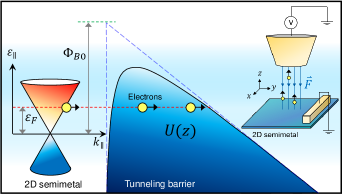
For field-induced electron emission, the tunneling potential barrier is modeled, with inclusion of the image charge effect across a dielectric interface, as , where is the intrinsic interface potential barrier height measured from zero-energy, , and is the dielectric constant of the substrate material (see Fig. 1 for the band diagram). The corresponding transmission probability can be accurately approximated as MG , , where , , and are correction factors for the image charge effect, and is the free electron mass (see SM for detailed derivations). Consider the typical case where there is only one subband around the Fermi level , Eq. (2) becomes,
| (3) |
where and denote the in-plane wavevector and energy components of the subband undergoing emission.
We now employ a generalized 2D anisotropic density of states (DOS) to solve Eq. (3). The DOS is defined as, where . Very generally, we can express the -differential as a two-variable polynomials, i.e. where is the expansion coefficient of the -th order in and -th order in , which yields the generalized 2D anisotropic DOS,
| (4) |
where and is an expansion coefficient that compactly contains the -integral SM . Combining Eqs. (3) and (4), the generalized thermal-field emission electrical current density from a 2D semimetal becomes where the -component is
| (5) |
which cannot be analytically solved except for the case of . An approximate analytical expression can be obtained by making the following ansatz. The term is replaced by where is a the correction factor for the -th order term since field emission is dominantly contributed by electrons residing around . By making the substitution , Eq. (5) becomes SM
| (6) |
where . The above integral can be analytically solved MG for t,
| (7) |
We evaluate the full numerical solution in Eq. (5) and the analytical approximation in Eq. (7) for to (Fig. 2). The approximate solution is in agreement with the full numerical results over the range of V/nm to V/nm with for to . From Eq. (7), we obtain the following scaling law,
| (8) |
Equation (8) represents a universal current-field-temperature scaling law for 2D semimetals as long as the DOS near can be captured by the generalized DOS model in Eq. (4). Equation (8) thus offer a simple unifying scaling law description of the field emission characteristics in two spatial dimensions. We derive the field emission characteristics for several representative 2D semimetals, including: (i) nodal point semimetal; (ii) graphene and its few-layer; (iii) Dirac semimetal near topological quantum phase transition; and (iv) nodal line semimetal, and show that their current-field-temperature scaling relation universally converges to Eq. (8) (summarized in Fig. 2).
III Case Studies of different 2D semimetals
Nodal point semimetal.– We first consider a generalized model of topological 2D nodal point semimetal with the effective Hamiltonian,
| (9) |
where is the in-plane wavevector, is the Pauli matrices, is a material-dependent parameter, and denotes the pseudospin vorticity. Equation (9) also describes the low-energy quasiparticles in -layer graphene of Bernal stacking configuration with , m/s and eV neto . Using the same procedure described above, Eq. (3) can be approximately solved as
| (10) |
The analytical approximate solution in Eq. (10) with the correction factor, for to based on the few-layer graphene band parameters exhibits good agreement with the full numerical results (Fig. 2).
Dirac semimetal near topological QCP.– We next consider a 2D Dirac semimetal near the topological quantum critical point (QCP) which can be captured by the effective Hamiltonian,
| (11) |
where and are band structure parameters. The system undergoes a topological quantum phase transition from a Dirac semimetal into a band insulator when is switched from to . In the semimetallic phase (), the thermal-field emission current density () is
| (12) |
where is a characteristic energy, and . The -integral, where , arises from the broken rotational symmetry of Eq. (11). The approximate solution Eq. (12) again exhibits good agreement with the full numerical results (Fig. 2), with at the QCP (i.e. ) and at the semimetallic phase (i.e. eV).
Nodal line semimetal.– In a 2D nodal line semimetal, the band touching of two bands extends from discrete nodal point into a continuous one-dimensional opened nodal line or closed nodal ring in phase space. We consider a representative 2D semimetal that hosts an isotropic equienergy nodal loop as described by the effective Hamiltonian,
| (13) |
where is a band inversion parameter. Solving Eq. (3) yields the approximate solution,
| (14) |
The above approximated form produces good agreement with the full numerical evaluation of Eq. (3) (Fig. 2) with the correction factor, for eV.
Graphene.– The thermal-field emission from graphene is described by the Dirac Hamiltonian, . The field emission current density is obtained as,
| (15) |
Here, the (also implicit in , and ) is a function of the applied electric field strength, i.e. yu_wf , due to the field-effect tunable Fermi level in graphene. Assuming a planar geometry and an initially undoped graphene with , we obtain . By evaluating Eq. (15) with , the full numerical solution is accurately reproduced with .
| 2D System | ||
|---|---|---|
| Generalized 2D band | ||
| Nodal point semimetal | ||
| Dirac semimetal near QCP | ||
| Nodal line semimetal | ||
| Graphene |
| 2D System | Fermi level dependence of | |
|---|---|---|
| Nodal point semimetal | ||
| Dirac semimetal near QCP | ||
| Nodal line semimetal | ||
| Graphene |
IV Discussions and Conclusions
Before conclusions, we make six remarks. Firstly, in the ‘cold’ field emission regime of , the scaling law in Eq. (8) becomes , which is in stark contrast to the FN-type cold field emission from bulk materials, . This difference directly suggests the breakdown of the FN model in 2D semimetals.
Secondly, the universal scaling law breaks down in the case of a non-dispersing 2D flat bands in 2D systems such as the Kagome mielke , Lieb lieb , - raoux and Archimedian lima lattices. For a flat band situated at , the thermal-field emission current densities is
| (16) |
which clearly deviates from Eq. (8). Such deviation also explains the reduced accuracy of Eq. (7) in approximating using Eq. (5) at large since each term in Eq. (4) corresponds to and thus a larger corresponds to a ‘flatter’ dispersion.
Thirdly, we remark that although the - scaling does not offer distinctive signature of band topology, the - scaling does contain rich scaling signatures for different band topologies (see Table I), which may offer a tool to probe the band topology in 2D systems.
Fourthly, the injection time parameter () of a 2D material solid/solid interface ranges from 10 ps (low-quality contact) to 0.1 ps (high-quality contact) depending on the contact quality sinha . For electron emission into vacuum, although no direct experimental measured values are available thus far, we expect to be larger than the 0.1 ps in 2D-material/vacuum interface since 2D material surface readily ‘couples’ to vacuum without additional interfacial defect generation. This aspect is unlike the case of solid/solid interfaces in which the fabrication process inevitably introduces interface defects that could reduce the charge injection efficiency. Importantly, our theoretical model shall provide a route for the experimentalist to additionally extract the parameter from the experimental current measurement data. The parameter shall thus provide an additional term for characterizing the performance and quality of a 2D-material-based field emitter.
Fifthly, we remark that the substrate can significantly affect the field emission characteristics of 2D field emitter, particularly the electronic properties of atomically-thin materials can be sensitively modified when they are in close proximity to an external materials vdw . Here we briefly discuss how various substrate are expected to affect the electron emission of 2D field emitters. For suspended 2D field emitter, the solid/solid interface defects are expected to be minimal due to the absence of a supporting substrate. In this case, the shorter injection time parameter is expected to lead to an improved magnitude of the field emission current in such emitter. Conversely for 2D field emitter lying on a dielectric substrate, the presence of a solid/solid supporting surface could lead to larger amount of interface defects which could reduce the charge injection efficiency into vacuum. For 2D materials lying on a 3D metal substrate, the field emission current is expected to be dominated by the 3D bulk metal as the electronic density of states of 3D metals are typically much larger than that of metallic 2D materials. Here, instead of being an electron emission source, 2D materials serve as a surface coating layer that modulates the 3D bulk metal surface properties, which could significantly modify the field emission properties of the 3D bulk metal jensen_DFT . We thus anticipate the substrate effects in 2D field emitter to form an important topic for future investigations.
Finally, we briefly comment on the edge emission from 2D materials, which is expected to differ significantly from the ‘face emission’ reported in this manuscript. The emission current density from edge is a 1D linear current density whose underlying transport physics and formalism is completely different from Eq. (2). Furthermore, the atomically sharp edge may generate strong field enhancement field and image charge effect that is drastically different from the case of a planar surface image . Importantly, the emitted electrons can also acquire a velocity component transversal to the edge emission direction. Such transversal electron emission can further complicate the formalism of edge emission. Microscopically, different edge termination configurations can affect the electronic properties of 2D materials edge . The edge emission characteristics is thus expected to be sensitively influenced by the atomic profile of the 2D material edges. The theoretical modeling of edge emission from 2D materials are thus expected to be a more complex problem that involves a multiphysics approach of first-principle atomistic material simulations, electrostatic modeling, and charge injection theory.
In summary, we have developed the theory of out-of-plane thermal-field electron emission from 2D semimetals. We demonstrated the existence of a universal current-field scaling law broadly applicable for a large variety of 2D semimetals with different band topologies. As thermal-field emission represents one of the key charge transport process across solid/vacuum and solid/solid interfaces, the universal scaling law developed here shall provide a simple useful theoretical tool for the study and the design of vacuum electronics, nanoelectronics, optoelectronics and the emerging concepts of spintronic roche , valleytronic ang4 and neuromorphic l_sun devices based on 2D materials and their van der Waals heterostructures, and shall offer a theoretical basis for the understanding of complex electron emission phenomena such as ultrashoft-pulsed laser-induced internal photoemission heide and photo-assisted hot carrier tunneling rezaeifar in the 2D Flatland.
V acknowledgments
This work is supported by A*STAR AME IRG (A2083c0057). Y.S.A is supported by the Singapore Ministry of Education Academic Research Fund Tier 2 (MOE-T2EP50221-0019).
References
- (1) R. H. Fowler, and L. Nordheim, ‘Electron emission in intense electric fields’, Proc. R. Sot. London Ser. A 119, 173 (1928).
- (2) John H. Booske, ”Plasma physics and related challenges of millimeter-wave-to-terahertz and high power microwave generation”, Physics of Plasmas 15, 055502 (2008).
- (3) P. Zhang, A. Valfells, L. K. Ang, J. W. Luginsland, and Y. Y. Lau, ‘100 years of the physics of diodes’, Appl. Phys. Rev. 4, 011304 (2017).
- (4) Peng Zhang, Yee Sin Ang, Allen L. Garner, Ágúst Valfells, J. W. Luginsland, and L. K. Ang , ”Space–charge limited current in nanodiodes: Ballistic, collisional, and dynamical effects”, Journal of Applied Physics 129, 100902 (2021).
- (5) W. J. Chan, C. Chua, Y. S. Ang and L. K. Ang, ”Field Emission in Emerging Two-Dimensional and Topological Materials: A Perspective,” in IEEE Transactions on Plasma Science (in press, 2022, doi: 10.1109/TPS.2022.3173469).
- (6) Yee Sin Ang, Liemao Cao, and Lay Kee Ang, “Physics of Electron Emission and Injection in Two-Dimensional Materials: Theory and Simulation”, InfoMat 3, 502-535 (2021).
- (7) A. H. Castro Neto, F. Guinea, N. M. R. Peres, K. S. Novoselov, and A. K. Geim, ‘The electronic properties of graphene’, Rev. Mod. Phys. 81, 109 (2009).
- (8) V. K. Sangwan, and M. C. Hersam, ‘Electronic Transport in Two-Dimensional Materials’, Annu. Rev. Phys. Chem. 69, 299 (2018).
- (9) M. I. Katsnelson, K. S. Novoselov, and A. K. Geim, ‘Chiral tun‘nelling and the Klein paradox in graphene’, Nat. Phys. 2, 620 (2006).
- (10) K. S. Novoselov, E. McCann, S. V. Morozov, V. I. Fal’ko, M. I. Katsnelson, U. Zeitler, D. Jiang, F. Schedin, and A. K. Geim, ‘Unconventional quantum Hall effect and Berry’s phase of in bilayer graphene’, Nat. Phys. 2, 177 (2006).
- (11) C. L. Kane, and E. J. Mele, ‘Quantum Spin Hall Effect in Graphene’, Phys. Rev. Lett. 95, 226801 (2005).
- (12) D. Xiao, W. Yao, and Q. Niu, ‘Valley-Contrasting Physics in Graphene: Magnetic Moment and Topological Transport’, Phys. Rev. Lett. 99, 236809 (2007).
- (13) M. S. Rudner, and J. C. W. Song, ‘Self-induced Berry flux and spontaneous non-equilibrium magnetism’, Nat. Phys. 15, 1017 (2019).
- (14) Y. S. Ang, Y. Chen, C. Tan, and L. K. Ang, ‘Generalized High-Energy Thermionic Electron Injection at Graphene Interface’, Phys. Rev. Appl. 12, 014057 (2019).
- (15) Y. S. Ang, H. Y. Yang, and L. K. Ang, ‘Universal Scaling Laws in Schottky Heterostructures Based on Two-Dimensional Materials’, Phys. Rev. Lett. 121, 056802 (2018).
- (16) Y. S. Ang, and L. K. Ang, “Current-temperature scaling for a Schottky interface with non-parabolic energy Dispersion”, Phys. Rev. Applied 6, 034013 (2016).
- (17) Shijun Liang, and L. K. Ang, “Electron Thermionic Emission from Graphene and thermionic energy convertor”, Phys. Rev. Applied 3, 014002 (2015).
- (18) M. Trushin, ‘Theory of photoexcited and thermionic emission across a two-dimensional graphene-semiconductor Schottky junction’, Phys. Rev. B 97, 195447 (2018).
- (19) M. Trushin, ‘Theory of thermionic emission from a two-dimensional conductor and its application to a graphene-semiconductor Schottky junction’, Appl. Phys. Lett. 112, 171109 (2018).
- (20) O. W. Richardson, ‘Some applications of the electron theory of matter’, Phil. Mag. 23, 594 (1912); S. Dushman, ‘Electron emission from metals as a function of temperature’, Phys. Rev. 21, 623 (1923).
- (21) K. L. Jensen, Introduction to the Physics of Electron Emission, Wiley (2017).
- (22) W. Schottky, Z. Phys. 15, 872, (1923); L. W. Nordheim, Proc. R. Soc. London, Ser. A 121, 626 (1928).
- (23) S. M. Sze, and K. K. Ng, Physics of Semiconductor Devices, Wiley-Interscience, 3rd Edition (USA, 2007).
- (24) J.-W. Han, M.-L. Seol, D.-I. Moon, G. Hunter, and M. Meyyappan, ‘Nanoscale vacuum channel transistors fabricated on silicon carbide wafers’, Nat. Electron. 2, 405 (2019).
- (25) E. L. Murphy, and R. H. Good, Jr., ‘Thermionic emission, field emission, and the transition region’ Phys. Rev. 102, 1464 (1956).
- (26) R. E. Burgess, H. Kroemer, and J. M. Houston, ‘Corrected values of Fowler-Nordheim field emission functions and , Phys. Rev. 90, 515 (1953).
- (27) R. Stratton, ‘Theory of field emission from semiconductors’, Phys. Rev. 125, 67 (1962).
- (28) R. G. Forbes, ‘Simple good approximations for the special elliptic functions in standard Fowler-Nordheim tunneling theory for a Schottky-Nordheim barrier’, Appl. Phys. Lett. 89, 113122 (2006).
- (29) K. L. Jensen, P. G. O’Shea, and D. W. Feldman, ‘Generalized electron emission model for field, thermal, and photoemission’, Appl. Phys. Lett. 81, 3867 (2002).
- (30) A. Kyritsakis and J. P. Xanthakis, ‘Derivation of a generalized Fowler-Nordheim equation for nanoscopic fieldemitters’, Proc. R. Soc. A 471, 20140811 (2015).
- (31) S.-D. Liang, and L. Chen, ‘Generalized Fowler-Nordheim theory of field emission of carbon nanotubes’, Phys. Rev. Lett. 101, 027602 (2008).
- (32) X. Wei, Y. Bando, and D. Golberg, ‘Electron emission from individual graphene nanoribbons driven by internal electric field’, ACS Nano 6, 705 (2012).
- (33) S. B. Fairchild, T. A. de Assis, J. H. Park, M. Cahay, J. Bulmer, D. E. Tsentalovich, Y. S. Ang, L. K. Ang, J. Ludwick, T. C. Back, and M. Pasquali, “Strongly anisotropic field emission from highly aligned carbon nanotube films”, J Appl. Phys. 129, 125103 (2021).
- (34) H. S. Sim, S. P. Lau, H. Y. Yang, L. K. Ang, M. Tanemura, and K. Yamaguchi, “Reliable and flexible carbon nanofibers based all plastic field emission devices”, Appl. Phys. Lett. 90, 143103 (2007).
- (35) H. S. Sim, S. P. Lau, and L. K. Ang, “Field emission from a single carbon nanofiber in a sub-100 nm gap”, Appl. Phys. Lett. 93 023131 (2008).
- (36) Y. S. Ang, S.-J. Liang, and L. K. Ang, ‘Theoretical modeling of electron emission from graphene’, MRS Bulletin 42, 505 (2017).
- (37) G. Eda, H. E. Unalan, N. Rupesinghe, G. A. J. Amaratunga, and M. Chhowalla, ‘’Field emission from graphene based composite thin films, Appl. Phys. Lett. 93, 233502 (2008).
- (38) M. Qian, T. Feng, H. Ding, L. Lin, H. Li, Y. Chen, and Z. Sun, ‘Electron field emission from screen-printed graphene films’, Nanotechnology 20, 425702 (2009).
- (39) Z.-S. Wu, S. Pei, W. Ren, D. Tang, L. Gao, B. Liu, F. Li, C. Liu, and H.-M. Cheng, ‘Field emission of single-layer graphene films prepared by electrophoretic deposition’, Adv. Mater. 21, 1756 (2009).
- (40) Z. Xiao, J. She, S. Deng, Z. Tang, Z. Li, J. Lu, and N. Xu, ‘Field electron emission characteristics and physical mechanism of individual single-layer graphene’, ACS Nano 4, 6332 (2010).
- (41) U. A. Palnitka, R. V. Kashid, M. A. More, D. S. Joag, L. S. Panchakarla, and C. N. R. Rao, ‘Remarkably low turn-on field emission in undoped, nitrogen-doped, and boron-doped graphene’, Appl. Phys. Lett. 97, 063102 (2010).
- (42) H. Yamaguchi, K. Murakami, G. Eda, T. Fujita, P. Guan, W. Wang, C. Gong, J. Boisse, S. Miller, M. Acik, K. Cho, Y. J. Chabal, M. Chen, F. Wakaya, M. Takai, and M. Chhowalla, ‘Field emission from atomically thin edges of reduced graphene oxide’, ACS Nano 5, 4945 (2011).
- (43) Q. Ma, T. I. Andersen, N. L. Nair, N. M. Gabor, M. Massicotte, C. H. Lui, A. F. Young, W. Fang, K. Watanabe, T. Taniguchi, J. Kong, N. Gedik, F. H. L. Koppens and P. Jarillo-Herrero, ‘Tuning ultrafast electron thermalization pathways in a van der Waals heterostructure’, Nat. Phys. 12, 455 (2016).
- (44) F. Rezaeifar, R. Ahsan, Q. Lin, H. U. Chae, and R. Kapadia, ‘Hot-electron emission processes in waveguide-integrated graphene’, Nat. Photon. 13, 843 (2019).
- (45) C.-K. Huang, Y. Ou, Y. Bie, Q. Zhao, and D. Yu, ‘Well-aligned graphene arrays for field emission displays’, Appl. Phys. Lett. 98, 263104 (2011).
- (46) D. Ye, S. Moussa, J. D. Ferguson, A. A. Baski, and M. S. El-Shall, ‘Highly efficient electron field emission from graphene oxide sheets supported by nickel nanotip arrays’, Nano Lett. 12, 1265 (2012).
- (47) G. Wu, X. Wei, Z. Zhang, Q. Chen, and L. Peng, ‘A graphene-based vacuum transistor with a high ON/OFF current ratio’, Adv. Func. Mater. 25, 5972 (2015).
- (48) G. Wu, X. Wei, S. Gao, Q. Chen, and L. Peng, ‘Tunable graphene micro-emitters with fast temporal response and controllable electron emission’, Nature Commun. 7, 11513 (2016).
- (49) J. Xu, Q. Wang, Z. Tao, Z. Qi, Y. Zhai, S. Wu, X. Zhang, and W. Lei,‘Field emission of wet transferred suspended graphene fabricated on interdigitated electrodes’, ACS Appl. Mater. Interfaces 8, 3295 (2016).
- (50) A. Di Bartolomeo, F. Giubileo, L. Iemmo, F. Romeo, S. Russo, S. Unal, M. Passacantando, V. Grossi, and A. M. Cucolo, ‘Leakage and field emission in side-gate graphene field effect transistors’, Appl. Phys. Lett. 109, 023510 (2016).
- (51) X. Wei, Q. Chen, and L. Peng, ‘Electron emission from two-dimensional crystal with atomic thickness’, AIP Adv. 3, 042130 (2013).
- (52) S. Sun, L. K. Ang, D. Shiffler, and J. W. Luginsland, ‘Klein tunnelling model of low energy electron field emission from single-layer graphene sheet’, Appl. Phys. Lett. 99, 013112 (2011).
- (53) W. Wang, X. Qin, N. Xu, and Z. Li, ‘Field electron emission characteristic of graphene’, J. Appl. Phys. 109, 044304 (2011).
- (54) D. Jena, ‘Tunneling Transistors Based on Graphene and 2-D Crystals’, Proc. IEEE 101, 1585 (2013).
- (55) Wei Jie Chan, Yee Sin Ang, and L. K. Ang, “Thermal-field electron emission from three-dimensional Dirac and Weyl semimetals”, Phys. Rev. B 104, 245420 (2021).
- (56) Cherq Chua, Chun Yun Kee, Yee Sin Ang, and L. K. Ang, “Absence of Space-Charge-Limited Current in Unconventional Field Emission”, Phys. Rev. Appl. 16, 064025 (2021).
- (57) A. A. Burkov, M. D. Hook, and L. Balents, ‘Topological nodal semimetals’, Phys. Rev. B 84, 235126 (2011).
- (58) M. Moore, P. Surowka, V. Juricic, and B. Roy, ‘Shear viscosity as a probe of nodal topology’, arXiv:1912.07611v1 (2019).
- (59) B. Roy and M. S. Foster, ‘Quantum Multicriticality near the Dirac-Semimetal to Band-Insulator Critical Point in Two Dimensions: A Controlled Ascent from One Dimension’, Phys. Rev. X 8, 011049 (2018).
- (60) C. Fang, H. Weng, X. Dai, and Z. Fang, ‘Topological nodal line semimetals’, Chinese Phys. B 25 117106 (2016).
- (61) J. Wang, Y. Liu, K.-H. Jin, X. Sui, L. Zhang, W. Duan, F. Liu, and B. Huang, ‘Pseudo Dirac nodal sphere semimetal’, Phys. Rev. B 98, 201112(R) (2018).
- (62) J. Hu, S.-Y. Xu, N. Ni, and Z. Mao, ‘Transport of Topological Semimetals’, Annu. Rev. Mater. Res. 49, 207 (2019).
- (63) H.-P. Sun, and H.-Z. Lu, ‘Quantum Transport in Topological Semimetals under Magnetic Fields’, Front. Phys. 12, 127201 (2017); H.-P. Sun, and H.-Z. Lu, ‘Quantum Transport in Topological Semimetals under Magnetic Fields (II)’, Front. Phys. 14, 33405 (2019).
- (64) C. J. Tabert, J. P. Carbotte, and E. J. Nicol, ‘Optical and transport properties in three-dimensional Dirac and Weyl semimetals’, Phys. Rev. B 93, 085426 (2016).
- (65) J. P. Carbotte, ‘Optical response of a line node semimetal’, J. Phys.: Condens. Matter 29 045301 (2017).
- (66) S. Ahn, E. J. Mele, and H. Min, ‘ Electrodynamics on Fermi Cyclides in Nodal Line Semimetals’, Phys. Rev. Lett. 119, 147402 (2017).
- (67) C. M. Wang, H.-Z. Lu, and S.-Q. Shen, ‘Anomalous Phase Shift of Quantum Oscillations in 3D Topological Semimetals’, Phys. Rev. Lett. 117, 077201 (2016).
- (68) C. Li, C. M. Wang, B. Wan, X. Wan, H.-Z. Lu, and X. C. Xie, ‘Rules for Phase Shifts of Quantum Oscillations in Topological Nodal-Line Semimetals’, Phys. Rev. Lett. 120, 146602 (2018).
- (69) B. Roy, R.-J. Slager, and V. Juricic, ‘Global Phase Diagram of a Dirty Weyl Liquid and Emergent Superuniversality’, Phys. Rev. X 8, 031076 (2018).
- (70) S. Sur, and B. Roy, ‘Unifying Interacting Nodal Semimetals: A New Route to Strong Coupling’, Phys. Rev. Lett. 123, 207601 (2019).
- (71) S. Zhou, K. Chen, M. T. Cole, Z. Li, J. Chen, C. Li, and Q. Dai, ‘Ultrafast Field-Emission Electron Sources Based on Nanomaterials’, Adv. Mater. 31, 1805845 (2019).
- (72) S.-J. Liang, B. Cheng, X. Cui, and F. Miao, ‘Van der Waals Heterostructures for High‐Performance Device Applications: Challenges and Opportunities’, Adv. Mater. 1903800 (2019).
- (73) P.-C. Shen, C. Su, Y. Lin, A.-S. Chou, C.-C. Cheng, J.-H. Park, M.-H. Chiu, A.-Y. Lu, H.-L. Tang, M. M. Tavakoli, G. Pitner, X. Ji, Z. Cai, N. Mao, J. Wang, V. Tung, J. Li, J. Bokor, A. Zettl, C.-I. Wu, T. Palacios, L.-J. Li and J. Kong, ”Ultralow contact resistance between semimetal and monolayer semiconductors”, Nature 593, 211 (2021).
- (74) Sneha Banerjee, Liemao Cao, Yee Sin Ang, L. K. Ang, and Peng Zhang, “Reducing Contact Resistance in Two-Dimensional-Material-Based Electrical Contacts by Roughness Engineering”, Phys. Rev. Applied 13, 064201 (2020).
- (75) Liemao Cao, Guanghui Zhoi, Qingyun Wu, Shengyuan A. Yang, Hui Ying Yang, Yee Sin Ang*, and L. K. Ang*, “Electrical Contact between Ultrathin Topological Dirac Semimetal and Two-Dimensional Materials”, Phys. Rev. Applied 13, 054030 (2020).
- (76) A. Allain, J. Kang, K. Banergee, and A. Kis, ‘Electrical contacts of two-dimensional semiconductors’, Nature Mater. 14, 1195 (2015).
- (77) Y. Xu, C. Cheng, S. Du, J. Yang, B. Yu, J. Luo, W. Yin, E. Li, S. Dong, P. Ye, and X. F. Duan, ‘Contacts between two- and three-dimensional materials: Ohmic, Schottky, and - heterojunctions’, ACS Nano 10, 4895 (2016).
- (78) S. V. Meshkov, ‘Tunneling of electrons from a two-dimensional channel into the bulk’, Sov. Phys. JETP 64, 1337 (1986).
- (79) K. J. Russell, F. Capasso, V. Narayanamurti, H. Lu, J. M. O. Zide, and A. C. Gossard, ‘Scattering-assisted tunneling: Energy dependence, magnetic field dependence, and use as an external probe of two-dimensional transport’, Phys. Rev. B 82, 115322 (2010).
- (80) H. Zhu, J. Wang, Z. Gong, Y. D. Kim, J. Hone, and X.-Y. Zhu, ‘Interfacial charge transfer circumventing momentum mismatch at two-dimensional van der Waals heterojunctions’, Nano Lett. 17, 3591 (2017).
- (81) L. Britnell, R. V. Gorbachev, A. K. Geim, L. A. Ponomarenko, A. Mishchenko, M. T. Greenaway, T. M. Fromhold, K. S. Novoselov and L. Eaves, ‘Resonant tunnelling and negative differential conductance in graphene transistors’, Nat. Commun. 4, 1794 (2013).
- (82) L. Britnell, R. V. Gorbachev, R. Jalil, B. D. Belle, F. Schedin, A. Mishchenko, T. Georgiou, M. I. Katsnelson, L. Eaves, S. V. Morozov, N. M. R. Peres, J. Leist, A. K. Geim, K. S. Novoselov, and L. A. Ponomarenko, ‘Field-Effect Tunneling Transistor Based on Vertical Graphene Heterostructures’, Science 335, 947 (2012).
- (83) T. Roy, L. Liu, S. de la Barrera, B. Chakrabarti, Z. R. Hesabi, C. A. Joiner, R. M. Feenstra, G. Gu, and E. M. Vogel, ‘Tunneling characteriss in chemical vapor deposited graphene-hexagonal boron nitride-graphene junctions’, Appl. Phys. Lett. 104, 123506 (2014).
- (84) E. E. Vdovin, A. Mishchenko, M. T. Greenaway, M. J. Zhu, D. Ghazaryan, A. Misra, Y. Cao, S. V. Morozov, O. Makarovsky, T. M. Fromhold, A. Patanè, G. J. Slotman, M. I. Katsnelson, A. K. Geim, K. S. Novoselov, and L. Eaves, ‘Phonon-Assisted Resonant Tunneling of Electrons in Graphene–Boron Nitride Transistors’, Phys. Rev. Lett. 116, 186603 (2016).
- (85) D. Ghazaryan, M. T. Greenaway, Z. Wang, V. H. Guarochico-Moreira, I. J. Vera-Marun, J. Yin, Y. Liao, S. V. Morozov, O. Kristanovski, A. I. Lichtenstein, M. I. Katsnelson, F. Withers, A. Mishchenko, L. Eaves, A. K. Geim, K. S. Novoselov and A. Misra, ‘Magnon-assisted tunnelling in van der Waals heterostructures based on CrBr3’, Nat. Electron. 1, 344 (2018).
- (86) U. Chandni, K. Watanabe, T. Taniguchi, and J. P. Eisenstein, ‘Signatures of Phonon and Defect-Assisted Tunneling in Planar Metal-Hexagonal Boron Nitride-Graphene Junctions’, Nano Lett. 16, 7982 (2016).
- (87) See Supplemental Material for a discussion of , the explicit forms of and , and the detailed derivations of , , , and .
- (88) F. Xia, V. Perebeinos, Y.-M. Lin, Y. Wu, and P. Avouris, ‘The origins and limits of metal–graphene junction resistance’, Nat. Nanotechnol. 6, 179 (2011).
- (89) Sinha, and J.-U. Lee, ‘Ideal graphene/silicon Schottky junction Diodes’, Nano Lett. 14, 4660 (2014).
- (90) M. Massicotte, P. Schmidt, F. Vialla, K. Watanabe, T. Taniguchi, K. J. Tielrooij and F. H. L. Koppens, ‘Photo-thermionic effect in vertical graphene heterostructures’, Nature Commun. 7, 12174 (2016).
- (91) Y.-J. Yu, Y. Zhao, S. Ryu, L. E. Brus, K. S. Kim, and P. Kim, ‘Tuning the graphene work function by electric field effect’, Nano Lett. 9, 3430 (2009).
- (92) S. Roche, J. Åkerman, B. Beschoten, J.C. Charlier, M. Chshiev, S. P. Dash, B. Dlubak, J. Fabian, A. Fert, and M. Guimarães, ‘Graphene spintronics: the European Flagship perspective’, 2D Mater. 2, 030202 (2015).
- (93) Y. S. Ang, S. A. Yang, C. Zhang, Z. Ma, and L. K. Ang, ‘Valleytronics in merging Dirac cones: All-electric-controlled valley filter, valve, and universal reversible logic gate’, Phys. Rev. B 96, 245410 (2017).
- (94) L. Sun, Y. Zhang, G. Hwang, J. Jiang, D. Kim, Y. A. Eshete, R. Zhao, and H. Yang, ‘Synaptic Computation Enabled by Joule Heating of Single-Layered Semiconductors for Sound Localization’, Nano Lett. 18, 3229 (2018).
- (95) A. Mielke, ‘Ferromagnetic ground states for the Hubbard model on line graphs’, J. Phys. A: Math. Gen. 24, L73 (1991).
- (96) E. H. Lieb, ‘Two Theorems on the Hubbard Model’, Phys. Rev. Lett. 62, 1201 (1989).
- (97) A. Raoux, M. Morigi, J.-N. Fuchs, F. Piechon, and G. Montambaux, ‘From Dia- to Paramagnetic Orbital Susceptibility of Massless Fermions’, Phys. Rev. 111, 026402 (2011).
- (98) F. Castro de Lima, G. J. Ferreira, and R. H. Miwa, ‘Topological flat band, Dirac fermions and quantum spin Hall phase in 2D Archimedean lattices’, Phys. Chem. Chem. Phys. 21, 22344 (2019).
- (99) C. Heide, M. Hauck, T. Higuchi, J. Ristein, L. Ley, H. B. Weber, and P. Hommelhoff, ‘Attosecond-fast internal photoemission’, Nat. Photonics 14, 219 (2020).
- (100) C. C. Tho, et al, ’Cataloguing MoSi2N4 and WSi2N4 van der Waals Heterostructures: An Exceptional Material Platform for Excitonic Solar Cell Applications’, Adv. Mater. Interfaces 10, 2201856 (2023).
- (101) K. L. Jensen, D. Finkenstadt, A. Shabaev, S. G. Lambrakos, N. A. Moody, J. J. Petillo, H. Yamaguchi, and F. Liu, ’A photoemission moments model using density functional and transfer matrix methods applied to coating layers on surfaces: Theory’, J. Appl. Phys. 123, 045301 (2018).
- (102) Y. Lu, G. L. Liu, J. Kim, Y. X. Mejia, and L. P. Lee, ’Nanophotonic Crescent Moon Structures with Sharp Edge for Ultrasensitive Biomolecular Detection by Local Electromagnetic Field Enhancement Effect’, Nano Lett. 5, 119 (2005).
- (103) P. Cudazzo, I. V. Tokatly, and A. Rubio, ’Dielectric screening in two-dimensional insulators: Implications for excitonic and impurity states in graphane’, Phys. Rev. B 84, 085406 (2011).
- (104) Y.-W. Son, M. L. Cohen, and S. G. Louie, ’Energy Gaps in Graphene Nanoribbons’, Phys. Rev. Lett. 97, 216803 (2006).