Ultrafast photocurrent and absorption microscopy of few-layer TMD devices isolate rate-limiting dynamics driving fast and efficient photoresponse
Abstract
Despite inherently poor interlayer conductivity, photodetectors made from few-layer devices of 2D transition metal dichalcogenides (TMDs) such as WSe2 and MoS2 can still yield a desirably fast (90 ps) and efficient (40%) photoresponse. By combining ultrafast photocurrent (U-PC) and transient absorption (TA) microscopy, the competing electronic escape and recombination rates are unambiguously identified in otherwise complex kinetics. Both the U-PC and TA response of WSe2 yield matching interlayer electronic escape times that accelerate from 1.6 ns to 86 ns with applied -field to predict the maximum device PC-efficiency realized of 44%. The slope of the escape rates versus -field suggests out-of-plane electron and hole mobilities of 0.129 and 0.031 cm2/V respectively. Above 1011 photons/cm2 incident flux, defect-assisted Auger scattering greatly decreases efficiency by trapping carriers at vacancy defects. Both TA and PC spectra identify a metal-vacancy sub-gap peak with 5.6 ns lifetime as a primary trap capturing carriers as they hop between layers. Synchronous TA and U-PC microscopy show the net PC collected is modelled by a kinetic rate-law of electronic escape competing against the linear and nonlinear Auger recombination rates. This simple rate-model further predicts the PC-based dynamics, nonlinear amplitude and efficiency, over a 105 range of incident photon flux in few-layer WSe2 and MoS2 devices.
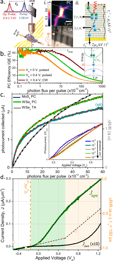
Photodetectors made from few-layer stacked, semiconducting 2D transition metal dichalcogenides (TMDs) like WSe2 and MoS2 can be remarkably fast (sub 100 ps) and efficient with internal quantum efficiencies (IQE, ) of photocurrent (PC) collected exceeding %.Yu2013 ; Massicotte2015 ; Lee2014 ; huang_lateral_2014 In Fig. 1a, our photodetector works by employing a parallel plate sandwich device geometry with a thin top-contact that uses either the built-in or applied voltage () to collects photoexcited electrons or holes. Stacked layers of WSe2 or MoS2 are only weakly coupled by van der Waals forces, resulting in very poor out-of-plane conductivity. To reconcile such weak interlayer coupling with the high PC-IQE and fast photoresponse seen in similar TMD devices, this work isolates the competing kinetics pathways of carrier recombination and interlayer escape in few-layer stacked TMD devices. Yu2013 ; Massicotte2015 ; Vogt:16 ; zhou_tunneling_2018
Measuring the electronic escape rates driving efficient PC collection remains challenging owing to complex intraband dynamics and defect-assisted Auger-scattering in stacked semiconductors like few-layer TMDs.zipfel_exciton_2019 ; selig_ultrafast_2019 ; zhao_evolution_2013 Presently, there exists no reliable in-situ time-resolved method that selectively isolates both the effective linear recombination () and electronic escape ( ) rates in the ultrafast regime. Transport based measurements lack the required time-resolution, while purely optical ultrafast measurements provide a convoluted weighted-average of all dynamics, offering no selectivity for rate-components that are relevant to PC production.Mueller2018 The high PC-IQE and nonlinear relaxation kinetics associated with TMDs give a nonlinear reduction in PC that can be time-resolved directly alongside purely optical measurements like transient absorption (TA) to isolate carrier extraction mechanisms and rates.
Even under low incident flux and continuous wave (CW) excitation, the interlayer electronic dynamics in TMDs are often dominated by defect-assisted Auger scattering that localize photocarriers in sub-gap defect sites.Wang2015a ; strait_high_2014 ; moody_exciton_2016 . For example, one defect-assisted Auger recombination process is depicted in Fig. 1b(inset) by showing electron-electron scattering to sub-gap defect states with defect density, . Such interactions have a rate coefficient, and a kinetic rate, that scales quadratically with electron or hole density, . Prior optical ultrafast studies show fast and slow Auger rate laws dominate the kinetic relaxation in few-layer TMDs over the range of photon fluxes employed.Yuan2015 ; li_auger_2018 ; yu_fundamental_2016 However at the lower photon fluxes practically relevant to TMD device operation, more complex kinetic rate models are proposed that fully describe the fast electronic scattering and thermalization within the indirect-gapped band structures of WSe2 and MoS2.he_competition_2018 ; Wang2015 ; Wang2015b While such complex rate laws are now required to rationalize the multi-component relaxations observed in optical TA-based measurements, it remains unclear which kinetic processes are practically relevant to PC-IQE and overall response times.merkl_ultrafast_2019 ; moody_exciton_2016 As shown in Fig. 1a, we will analytically test the adequacy of simpler kinetic rate models to identify which dynamics processes sufficiently predict the net PC-collected and response time in few-layer TMD-photodetectors.
By combining ultrafast photocurrent (U-PC) with transient absorption (TA) microscopy, this work identifies bottleneck-kinetic rate mechanisms that intrinsically limit the maximum PC-IQE achievable in few-layer TMD photodetectors. The integrated U-PC device response is thought to be selective for rate-limiting electronic dynamics forming the primary bottleneck for PC extraction.Graham2013 ; Gabor2012 ; Massicotte2015 ; Vogt:16 However, this assumption is untested and no robustly-used response-function for extracting first-principle kinetics from U-PC kinetics yet exists. Consequently, we employ synchronous E-field-dependent TA microscopy, to show how both the pure-optical and purely-electronic detection regimes independently predict the same high PC-generation efficiency and fast electronic escape times in TMD-based devices.
Experimental Analysis I: Modeling the nonlinear photoresponse of TMDs.
We began by fabricating photoconductive devices illustrated in Fig. 1a of few-layer WSe2 or MoS2 TMDs (see method details). The photocurrent signal was collected from both WSe2 and MoS2 devices by raster scanning a pulsed (160 fs) or continuous wave (CW), diffraction-limited spot resonant with the lowest, K-point transition. Optically translucent (See supplement S.1) metallic 16/2 nm Au/Ti layers formed excellent top-contact with a subset of devices fabricated. Each device shown in Fig. 1a is further divided into 6 distinct contact regions. Only devices generating a uniform strong PC signal such as shown in Fig. 1ai. were used for this study to help decouple contact and barrier issues. In Fig. 1ai. scanning PC microscopy spatial maps of a 69 layer WSe2 device shows strong, uniform PC over the sandwiched regions that is 2-3 orders of magnitude greater than any edge-PC signals around the peripheral leads. The corresponding TA scanning microcopy map shown in Fig. 1ai is sensitive to the carrier population remaining after at pulse delay time, 1 ps between pump and pulses resonant with the optical gap. Using these scanning maps, a 0.9-1.4 m laser spot size was localized on the device center for all PC and TA measurements. As depicted in Fig. 1aii (dashed arrows), TMDs placed between capacitively matched contacts have two modes of operation; i.e. either the photoexcited electron-hole pairs are extracted (low applied voltage, ) as a PC, or a photoconductive current between contacts is optically induced as the diode-like response turns-on at higher at higher .
Fig. 1b shows that as the incident photon flux per pulse increases by 104, the WSe2 device PC-IQE, drops precipitously (see supplement S.1 for IQE and EQE calculations). This drop suggests nonlinear rate kinetics are required to predict the PC amplitude above a photons/cm2 threshold. This threshold photon flux in PC-IQE further increases by a factor of 10 going from the unbiased (orange line) to biased (0.4 V, green line), and again to continuous wave (CW) illumination (0.4 V, red line).Massicotte2015 ; Yu2013 This shift is understood by noting the Auger recombination rate, , will increase both with carrier density (i.e. pulsed vs. CW) and as electron drift velocity slows when to enhance carriers present in the device. While the nonlinear PC-dependence in Fig. 1b-c has been previously attributed to Auger recombination processes, there exists no predictive analytic model linking the PC and optical responses widely reported in such TMD materials.
In agreement with the early few-layer TMD device studies by Yu et al.Yu2013 , Figs. 1b-c show a highly nonlinear PC response for resonant CW and pulsed excitation of both WSe2 and MoS2 devices. This motivates the inclusion of slow defect-assisted scattering Auger processes in our kinetic model for PC. Wang et al. show the nonlinear response has contributions from both fast Auger recombination with rate, and slower interlayer defect-assisted Auger recombination processes with rate , where is either the electron or hole densityWang2015a ; vialla_tuning_2019 .
Fast Auger processes occurs on a timescale commensurate with the interlayer electron-hole separation time, (see discussion).Poellmann2015 The rate law for slower defect-assisted Auger processes is written as where , and scales linearly with the constant metal or dichalcogenide vacancy defect concentration.
To model the nonlinear PC response in few-layer WSe2
and MoS2 photodetectors, we first consider a simplified kinetic rate law of the PC-efficiency-limiting rate processes. We approximate the total linear rate, involved in PC generation as the sum of the applied field-dependent electron/hole net escape rate, and linear recombination rate, . This approximation ignores explicit spatial and valley dependence. Collectively after electron-hole separation, the rate law for the time-evolution of electron or hole photocarriers density is simply,
| (1) | ||||
| (2) |
The above solution to the rate law predicts that carrier density grows nonlinearly with initial photocarrier density, .Yuan2017 In the low carrier density limit (), Eq. 2 gives the carrier density, growing linearly with initial carrier density (and incident photon flux). This purely linear PC-response region is clearly seen by the flat-region of Fig. 1b (and later again in Fig. 3b on a log-log scaling). Fig. 1c plots TA deferential reflectivity power dependence for the WSe2(gray line, right axis) and fits well to Eq. 2 (dashed black line).
Unless otherwise specified, the PC and TA signals are collected at resonant excitation at optical gap of WSe2 , and both signals evolve from a linear to nonlinear scaling with increasing photon incident flux (see Fig. 1b-c). To test if Eq. 1 predicts the interlayer PC response in TMDs, Fig. 1c (and 3b) we plots the integrated PC response over a 105 change in photon flux. The integrated photocurrent density, of electrons or holes is a spatial transport process traditionally defined through the diffusion coefficient , and any driving applied voltage.zipfel_exciton_2019 Alternatively, for few-layer devices we instead approximate in the time-domain by integrating time-dependent carrier density, given by in Eq. 2 and doing a time averaged over the mean electronic escape time, to get,
| (3) | ||||
| (4) |
This yields a simple, but highly predictive expression showing how the PC collected depends nonlinearly on the initial photoexcited carriers created (). In Fig. 1c (and again later in Fig. 3b), the red-dashed line fits to Eq. 4 show excellent agreement with PC spanning five orders of magnitude of photon-flux dependence for both TMD devices of 56 nm in WSe2 (green line) or 43 nm in MoS2 (blue line). The highly predictive nature of Eq. 2 and 4 suggest the simple rate law in Eq. 1 might sufficiently capture the rate-limiting kinetics germane to PC collection. This assertion will be further tested by ultrafast time-resolved PC and TA in section II.
For photogenerated carriers, the escapes rates have been previously approximated using the drift velocity, where is the out-of-plane electron or hole mobility, and is the mean distance to escape.Massicotte2015 ; Gabor2012 In the thin sandwich device capacitive geometry shown in Fig. 1a, the perpendicular E-field is determined as (see supplementary section for justification), where is the device open-circuit voltage. Solving for the electronic escape time, one obtains,
| (5) |
where is the mean distance of photocarrier transport to the contact Ti/Au contacts. AFM of the WSe2 device in Fig. 1ai. shows the total TMD layer thickness is L=56 nm. In Fig. 1c (inset), the combination of Eqs. 4 and 5, also simulates how the PC data scales with . Over the 104 range of photon flux shown, both the linear scaling, |, and the nonlinear scaling regions the dependent PC-response are also modelled well by combining Eq. 4 and 5 (red line fits).
The green line in Fig. 1d is the illuminated current density, and shows an inflective change at 0.55 V. The dark current, is 100x smaller than and exhibits diode-curve-like behavior for low . As PC-signals shown are detected by using lock-in detection, the weak, response is removed from all our signals to isolate only the photoresponse. There are two quasi-linear regimes in Fig. 1d (dashed black line fit) delineated by the green or orange background shading. Each region corresponds to PC dominated by photo-extraction or photoconduction, respectively. To compare PC to the purely optical response, on the right-axis of Fig. 1d, the orange squares show the amplitude of the TA differential reflectivity signal at a 160 ps. Interestingly, the purely optical TA signal also shows two quasi-linear regions, tracking the PC electronic signal closely.
When photoexcited carriers are directly extracted as a PC, electric field simulations suggest the mean escape distance is approximately .Massicotte2015 However for a photoconduction response, the electronic carriers must instead hop the device thickness between all layers. In Fig. 1d, the PC-response evolves to a photoconductive dominated response as the applied voltage, is swept from the open-circuity value, =-0.089 to 1.30 V. Revisiting the inset of Fig. 1c, one observes this evolving inflection-point in photocurrent density develops for photon flux below photon/cm2 where PC-collection becomes favorable over photoconduction. In the next section, the associated dynamic rates driving the complex PC response of Fig. 1 are obtained using a novel ultrafast time-domain analysis of on-chip PC and TA microscopy.
Experimental Analysis II: connecting ultrafast TA and PC electron escape dynamics with device efficiency and response time.
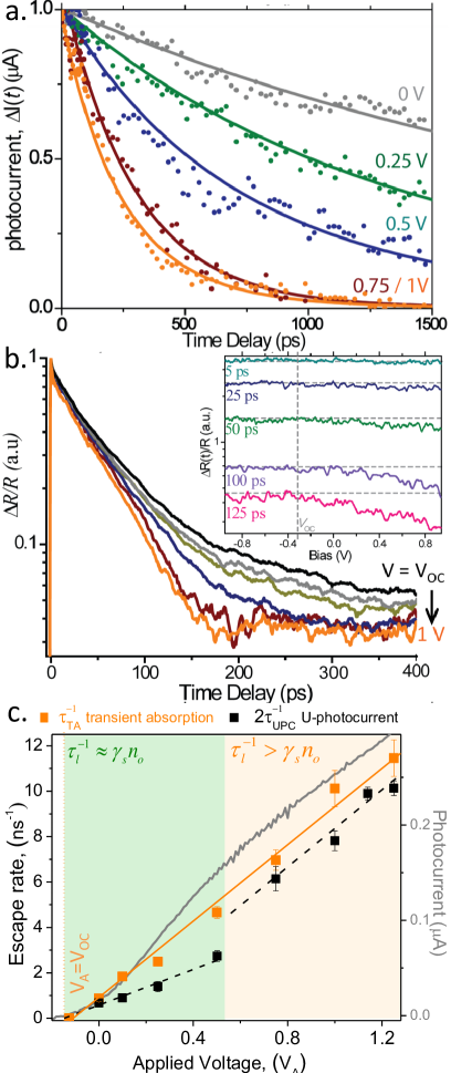
In section I, the simple kinetic rate law in Eq. 1 predicted both the photon-flux dependent PC and TA absorption amplitude better than any phenomenological power-law fits attempted (shown in supplement S.3).Massicotte2015 ; Wang2015 Resolution of kinetic rates pertinent to the PC response of few-layer TMDs, require both sub-100 ps time-resolution and selectivity for PC generating dynamic processes. Fig. 2 plots the ultrafast photocurrents (U-PC) concurrently measured with TA as in increases slowly from to 1.3 V. The results are all repeatable and how minimal impact from the small transport curve hysteresis. This synchronous optical and electronic detection-regime is important to isolate the ultrafast electron escapes rates from other recombination dynamics.
Prior works applying U-PC to graphene, carbon nanotubes, and similar 2D TMDs suggest U-PC is predominately sensitive to the competing kinetic rates that limit PC detection (e.g. extraction vs. recombination).Graham2013 ; Graham2013a ; Gabor2012 ; Wang2015 ; Massicotte2015 ; Vogt:16 Figure 2a shows the normalized U-PC kinetics markedly accelerate with increasing applied voltage, consistent with faster carriers extraction. Similar U-PC kinetics on WSe2 photodetectors were first reported by Massicotte et. al. and Vogt et al. in 2016.Massicotte2015 ; Vogt:16 However, there remains no independently-verified response function that reliably extracts the first-principle kinetic rate constants from the U-PC response.
Motivated by the highly predictive PC-response of Eqn. 3-4 in section I, a related U-PC response function is obtained by direct piecewise integration of about the delay-time, to give a time-correlated U-PC response function,
| (6) |
This equation with Eqn. 3 for n(t), simulates the normalized U-PC data with only two free-parameters after the background PC signal, given by is subtracted. Fig. 2a plots the theoretical U-PC curves after the two-free parameters were optimized, as they capture the kinetic response better than exponential fits commonly to U-PC in the literature. Nonetheless, the timescales extracted are not radically different than an ad-hoc exponential fit analysis. All data and simulation are normalized to peak maximum to compare dynamics (see supplement section S.4 for examples of uncorrected raw data).
To independently verify the U-PC response function proposed in Eq. 6, we compare the U-PC rates extracted in Fig. 2a to the outwardly much-faster synchronously obtained TA kinetics plotted in Fig. 2b. Figure 2b shows the resonantly excited ( point) TA microscopy relaxation increases markedly with applied voltage (), but only in the second decay component. Figure 2b (inset) clearly shows the raw TA signal-amplitude strongly decreases with , but only the 75-125 ps range associated with the second decay component. As Eq. 5 correctly, the slowest TA relaxation is not observed at =0, but instead at the open-circuity voltage, where no net-PC is collected. By definition, only TA (not U-PC) can be collected at when no net carriers are extracted. A least square deconvolution fit of the TA to Eqn. 2 gives ps, and represents the linear recombination rate. Combined with the high (up to 44%) IQE of the device, TA kinetics in Fig. 2b accelerate as the carrier are extracted from the device at a mean electronic escape rate . Strikingly in Fig. 2c (orange squares), the TA escape rates increase linearly with after the linear recombination rate term is subtracted. Obtained by fitting of U-PC kinetics to Eq. 6, Fig. 2c also plots the rates obtained from a nm thick WSe2 device. The electron or hole escape rates, in Fig. 2c all increase with according to Eqn. 5. The fits shown yield slopes further estimate the electron and hole mobilities using Eqn. 5 (see Table 1).
Interestingly, Fig. 2c shows that the -field-dependent TA optical escape rates (orange circles) agree well with the rates obtained from our U-PC response function (black squares). The agreement of optical and electronic responses at high , suggests the U-PC response function proposed in Eqn. 6 provides rate-limiting escape kinetics for PC-generation for our TMD devices.
| method | l | |||||||
| TA | 1.1 | 28 | 82 | 92 | 44 | 341 | 0.128 | 0.52 |
| 0.5 | 28 | 1430 | - | - | 78 | 0.031 | - | |
| 1.1 | 56 | 248 | - | 52 | 245 | 0.121 | 0.43 | |
| PC at 0 V | 0 | 28 | - | - | - | - | - | 0.43 |
| PC at 1 V | 1 | 56 | - | - | - | - | - | 0.44 |
| (units) | V | nm | ps | m/s | cm2/Vs |
In the time-domain, PC-generation efficiency() in Fig. 1b can be approximated by a ratio of competing kinetic rates given by, . When the defect assisted-Auger scattering rate is small at low photon fluence, . In Fig. 2c, the WSe2 device intrinsic photocurrent efficiency increases with applied voltage to yield 52% prediction TA kinetics and 43% from U-PC kinetics. The figures of merit are summarized in Table 1.0, and show the U-PC matches the actual device performance better than TA. The higher efficiency predicted by of TA is the likely result of overestimating the actual electron drift length, l as . At high for U-PC, the electrons must traverse the full length of the device for photoconduction so is known accurately resulting in more accurate efficiency prediction.
.1 DISCUSSION
WSe2 in-plane conduction can approach >350 cm2V-1s-1kim_enhanced_2016-1 ; Lee2014 , whereas the out-of-plane conduction is smaller. Nonetheless, devices made using the interlayer out-of plane conduction mode are often more efficient than reported in-plane conducting devices.Lee2014 The combined large multilayer absorption, short (20-30 nm) escape lengths and long recombination times collectively help TMD achieve high PC-IQE. However, high defect densities, common in TMDs can negate this advantage owing to intrinsically slow electronic carrier drift velocities measured up to 250 m/s (even under high applied voltages, see Table 1.0) where . During interlayer drift, defect-assisted Auger recombination dominates when the incident photon flux is high-enough () enough for carrier scattering (e-e, e-h, h-h) to defect sites such as W-vacancies. Koperski2015 ; He2015
Prior optical ultrafast studies all agree TMDs relaxation dynamics are often dominated by defect-assisted Auger processes. wang_ultrafast_2015-1 ; strait_high_2014 ; Wang2015a ; ovesen_interlayer_2019 ; selig_ultrafast_2019 In 2016, Massicotte et al. Massicotte2015 reported that stacked WSe2 devices can have both 30% and fast ( ps), picosecond electron escape times, . Even with our new analysis and the addition of TA, our results and rates obtained still closely match the early seminal works Massicotte2015 ; Vogt:16 of U-PC for similar thickness WSe2 devices. As suggested by spectra and bandstructure plotted in Fig. 3a and c, a complete description of the relaxation pathways of resonantly excited WSe2 must rigorously track transient electron and holes population at all low-lying symmetry points () and the defect states. Such complete kinetic models have been the subject of many transient optical absorption and time-resolved photoluminescence studies.Wang2015a ; moody_microsecond_2018 ; zhu_enhancement_2018 ; kaviraj_physics_2019 ; Pogna2016 Near time zero, fast Auger processes are indicated by strongly square root scaling of the TA signals on photon flux is observed.he_competition_2018 After excitation, the electron-hole pairs dissociate at a rate, by intervalley themalization or undergo fast-Auger scattering at rate with a kinetic rate of electron-hole pairs written asAmani2015 ; Borzda2015 ; Yu2016 ; Arora2015 ; Mouri2014 ; Rivera2015 ,
| (7) |
At very short delay times, our TA kinetic decay show signatures of the above kinetic rate law associated with electronic scattering and dissociation (e.g. see supplemental section confirming fast photon-flux dependent TA kinetics). In particular, at shot delays the initial kinetics accelerate with the incident photon flux. Fast electron-hole dissociation it is not a rate-limiting process for PC-generation for few-layer WSe2 and so our kinetic treatment of the carrier dynamics after dissociation used in Eq. 1-2 is justified.moody_exciton_2016 ; moody_microsecond_2018
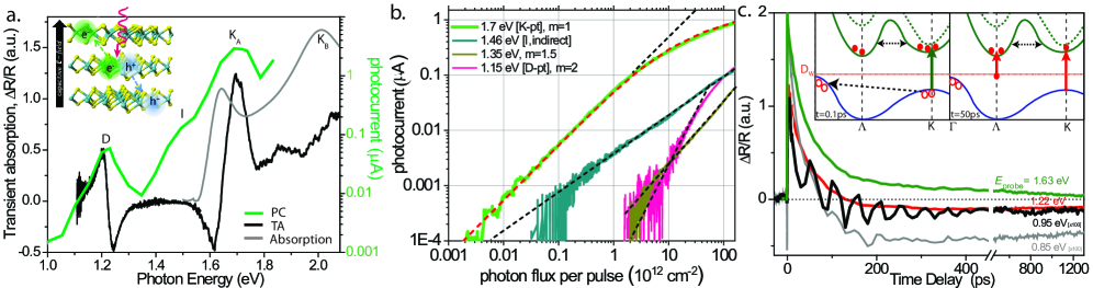
In Fig. 3a the linear absorption (gray), TA (black) and PC (green) spectra of a WSe2 device are plotted over a 1.0 to 2.1 eV spectral range. At 1.68 eV both the TA transient bleach and the linear absorption peak strongly at resonant KA-point transition. Unexpectedly, we also observe a sub-gap excited state absorption (ESA) peak centered at at 1.21 eV. While such sub-gap peaks are not present in our linear absorption, the PC-spectrum in Fig. 3a (green line, log-scale on right axis) has a matching sub-gap peak visible on semi-log scaling. The PC spectrum further has a labelled shoulder-peak, I that matches the indirect bandgap of WSe2 at 1.53 eV.kaviraj_physics_2019
To understand the origin of PC and TA response at the labeled D-peak at 1.21 eV, a PC laser flux power-dependence is plotted for each peak-excitation energy in Fig. 3b (log-log scaling). Upon resonant excitation at , the red-dashed line fit to Eq. 4 remarkably captures the PC-response over five-orders of magnitude and clearly delineating the onset on of nonlinear-PC response at 1012 photons/cm2 flux. Sun2014a ; Zhao2013 For sub-gap region excitation, Fig. 3b shows a PC-response that is superlinear, increasing quadratically with photon flux (slope m=2).zhu_enhancement_2018 ; massicotte2016 While direct optical excitation of defect states is generally not possible owing to momentum-matching restriction, a weakly allowed two-photon excitation is proposed. Figure 3b supports a two-photon excitation by the characteristic quadratic increase in PC response with photon flux only for the energy matching the ESA TA D-peak in Fig 3a. Comparison with prior DFT simulations of WSe2 cells of W metal-metal vacancies suggest a likely origin of this sub-gap defect peak as depicted Fig. 3c.wu_atomic_2018 ; moody_microsecond_2018 ; fang_strong_2014
TA relaxation dynamics shown in Figs. 3-4 vary greatly depending upon the energetic window of the band-structure probed after resonant excitation. TA shown in Fig. 2b and 3c are always summation of all electronic kinetic pathways in WSe2 for a selected probe window. Fig. 3c (inset) schematically shows multi-layer WSe2 bandstructure. In TA, the holes are largely scattered out of the resonant spectral probe window to the -point, making resonantly excited TA predominately sensitive to thermalized electron (vs. hole) population. Conversely, as holes have lower mobility in WSe2, photoextraction is strongly impacted the hole escape rate. Accordingly, our U-PC escape rates plotted in Fig. 2c at low applied fits to Eq. 6 and the slope estimates the out-of-plane hole mobility of 0.031 cm2/(Vs). The hole mobility is x smaller than the electrons, roughly consistent with its larger effective mass as indicated by DFT of the valence band maximum curvature.wu_atomic_2018 ; fang_strong_2014 At higher , the device is predominately in photoconduction mode and U-PC is instead limited by the photoinduced-electron lifetime. In Fig. 2c, the slope of both TA and U-PC escape rate agree giving identical estimates of the electron mobility of 0.128 cm2/(Vs). This time-domain values of the mobility agree reasonably with literature and our transport-based estimate of our device.moody_exciton_2016 ; kim_enhanced_2016 ; fang_strong_2014
Figure 3c plots the relaxation rates associated with-using sub-gap probe window to access the defect state lifetime. For sub-gap probe energies below the D-peak resonance, the TA response is small (<100x), and the signal in Fig. 3c at 0.85 and 0.95 eV is predominantly attributed to the long-lived transient thermal response WSe2. This is supported by the incidental presence of a strong TA beat period of 44 ps that further predicts a speed of sound of 2650 m/s in WSe2 which is faster than slower interlayer electronic hopping velocities estimated in Table 1.0.
As previously shown, defect-assisted Auger scattering dominates TA signal above photons/cm2. Figure 4a plots the fluence-dependent TA kinetics of a resonantly excited 69-layer WSe2 device at such high pump-fluences. The long ground state recovery component is 5.6 ns and likely attributable to defect relaxation and grows in relative amplitude with photon flux. This coincides with the rate of defect-assisted Auger scattering growing with carrier density, n.
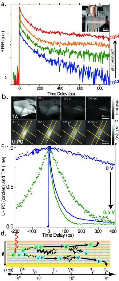
Figs. 4b-d summarize our combined TA and U-PC microscopy-measurement response as a function of time, space and applied voltage. A cartoon time-line in Fig. 4d captures the dominant photocurrent generating dynamic pathways; from light absorption to photocurrent collection. The mechanisms suggested in Fig. 1aii anf 4d are supported by simultaneous measurement of both TA and U-PC responses. Taken together, they selectively isolate the PC-relevant kinetic rates of Auger recombination (), linear recombination (), and mean escape rate, . For much thiner, TMD stacks even faster electronic extraction times (down to 50 ps) are reported by Massicotte et al in similar few-layer WSe2 devices using graphene-based contacts.Massicotte2015 Quantitatively similar results are obtained here by using a first principle kinetic model. While our model is crude to those needed for prior TA studies, we show it is sufficient for predicting PC generation by direct real-time comparison with TA measurements.Wang2015a ; vialla_tuning_2019 ; li_auger_2018 ; Yuan2015
The agreement between the U-PC rates and E-field-dependent TA rates in Fig. 2c independently validates that the proposed U-PC response function in Eq. 6 correctly retrieves first principle kinetics.Palummo2015 ; Cui2014 ; bakulin_ultrafast_2016
In summary, photodectors of few-layer semiconducting TMDs like WSe2 have low out-of-plane mobilities, and the slow drift velocities make defect-assisted Auger-scattering a bottleneck to PC-collection even under CW excitation. Going forward, this combined TA+U-PC microscopy approach suggests a promising, new way to screen materials for the maximal device PC-collection efficiency by isolating the ultrafast electronic rates that are rate-liming to photocarrier extraction.bakulin_ultrafast_2016
Conclusions:
Recent time-domain studies of stacked WSe2 show TMD devices can be both efficient and fast despite very low out-of-plane mobility.Vogt:16 ; Massicotte2015 Using a first-principle kinetic model involving defect-assisted Auger recombination the nonlinear PC response in Fig. 1c and 3b can be accurately predicted and fit better commonly power-law approximations. As the applied voltage increases the TA and U-PC extracted escape times increase linearly as , from 86 ps to 1.6 ns. Using these rates, a simple kinetic rate model of carrier escape and defect-assisted Auger recombination sufficiently models the device PC-IQE and e nonlinear PC-power dependence over a change in photon flux.
Matching synchronously obtained TA results in Fig. 2c, provide independent confirmation that the U-PC first-principle kinetic response function proposed in Eq. 6 analytically extracts the E-field-dependent escape rate. The ratio of competing ultrafast rates extracted from TA and U-PC predict an 45% (PC-IQE), suggesting our TMD photodetectors are intrinsically limited by 92 ps recombination time extracted at open-circuit voltage. This closely matches the 44% IQE originally measured on our a 56 nm thick WSe2 devices in Fig. 1b. Both optical and electronic methods gave independently agreeing electronic escape times, and provided out-of-plane electron and hole mobilities of 0.129 and 0.031 cm2/V respectively for WSe2. The large absorption coefficient, short escape lengths and the suppressed recombination of carriers collectively explain why WSe2 -based photosensors can still be both fast ( ps) and efficient despite low out-of-plane carrier mobility and strong Auger recombination process. By combining -field dependent ultrafast photocurrent with transient absorption microscopy we idenified the dominant kinetic bottlenecks inhibiting photocurrent efficiency for stacked few-layer TMD semiconductors phtodetectors. This approach may further help indentify the maximum quantum efficiency in other promising materials where electron extraction is kinetically favorable over recombination.
I Method Details:
Device preparation: 150 nm thick gold contact pad are patterned on a silicon wafer. Both WSe2 and MoS2 was mechanically exfoliated and inspected optically to identify thick that was confirmed by atomic force microscopy (AFM). Optimal thicknesses ranged from 50 to 100 layers such that % of incident light is absorbed, but the mean path for electron escape is short enough to efficiently collect.Yu2013 ; huang_lateral_2014 TMD samples were then spun-cast with MMA polymer, transferred mechanically onto the gold electrodes and released thermally after careful cleaning steps optimize contacts. Finally, an optically translucent top gate of titanium/gold (2nm/16 nm) was deposited along the top of the exfoliated TMD material. Eight independently working devices with strong, uniform PC response as shown in Fig. 1a were studied, and all gave similar result when the stack-layer thickness was accounted for.
Ultrafast photocurrents and transient absorption microscopy: After resonant optical pumping of the -point transition shown in Fig. 3c, the transient spectra and kinetics are measured using confocal scanning U-PC and TA microscopy.hartland2010 Collinear pump-and probe pulses were obtained from two independently tunable outputs of an ultrafast Ti:Sapphire oscillator (Coherent Chameleon Ultra II, 80 MHz) pumping an optical parametric oscillator (APE-Compact). Spectrally resolved TA spectral measurements resonantly pump the K-point transition resonance at 780 nm, and a white-light supercontinuum probe was used to capture both transient spectra. Cross-correlation of the pump and probe after the objective yielded a pulse duration of about 160 fs.
After a mechanical delay stage, both the pump and the probe beams were aligned in a collinear geometry, raster-scanned by piezo-scanning mirror and coupled into a confocal scanning microscope via a 50X IR-region enhanced, achromatic objective (NA= 0.65). Transient absorption signals were detected by measuring the probe beam on with a TE cooled InGaAs detector connected to a Zurich HF2-LI lock-in amplifier with current preamplifier. The pump beam was modulated at either a 25 kHz using an acousto-optical (AO-modulator (Gooch & Housego) to enable high-frequency lock-in detection of the differential reflectivity, . Frequency was swept to ensure beam modulation frequency is independent of the photoresponse measured. Appropriate optical filters or Acton monochromator were used in front of the detector to block the pump beam and select probe spectral window. The pump and probe spot sizes on the sample were determined to 1.5 m, by fitting to a confocal scanning reflection profile of lithographic gold pad edges. All the measurements were done at 295 K. The probe power was fixed at ( photons/cm2 ) for the pump power dependence measurements.
The steady-state scanning photocurrent geometry discussed above is modified to accommodate simultaneous transient absorption and U-PC measurements. Specifically, a linear delay stage is added to control the relative timing of the two incident laser pulses (one at 780 nm and one 810 nm to present pulse optical interferometry) which are aligned in a collinear geometry before a piezo scanning mirror (PI, ) and coupled into the microscope (Olympus BX-61WI). Both U-PC and TA microscopy signals are collected as a function of delay-time using lock-in amplifiers and amplitude-modulation the two beam lines shown in Fig. 1a. The ultrafast photoresponse was demodulated by either single or difference frequency chopping mode. Photon-flux dependent measurements used a motorized polarizer-waveplate combination to study the TA and PC response over a continuous range.
Acknowledgements: This work acknowledges the Spectroscopy Society of Pittsburgh, NSF MRI grant 1920368 and Oregon Best for project support. S.-F. Shi acknowledges support by AFOSR through grant No. FA9550-18-1-0321
References
- (1) W. J. Yu, Y. Liu, H. Zhou, A. Yin, Z. Li, Y. Huang, and X. Duan, oct , 2013, 8(12), 952–958.
- (2) M. Massicotte, P. Schmidt, F. Vialla, K. G. Schädler, A. Reserbat-Plantey, K. Watanabe, T. Taniguchi, K. J. Tielrooij, and F. H. L. Koppens, January , 2016, 11(1), 42–46.
- (3) C.-H. Lee, G.-H. Lee, A. M. van der Zande, W. Chen, Y. Li, M. Han, X. Cui, G. Arefe, C. Nuckolls, T. F. Heinz, J. Guo, J. Hone, and P. Kim, Nature Nanotechnology, 2014, 9(9), 676–681.
- (4) C. Huang, S. Wu, A. M. Sanchez, J. J. P. Peters, R. Beanland, J. S. Ross, P. Rivera, W. Yao, D. H. Cobden, and X. Xu, December , 2014, 13(12), 1096–1101.
- (5) K. Vogt, S. Shi, F. Wang, and M. W. Graham In International Conference on Ultrafast Phenomena, p. UW2A.3. Optical Society of America, 2016.
- (6) X. Zhou, X. Hu, S. Zhou, H. Song, Q. Zhang, L. Pi, L. Li, H. Li, J. Lü, and T. Zhai, Advanced Materials, 2018, 30(7), 1703286.
- (7) J. Zipfel, M. Kulig, R. Perea-Causín, S. Brem, J. D. Ziegler, R. Rosati, T. Taniguchi, K. Watanabe, M. M. Glazov, E. Malic, and A. Chernikov, November , 2019.
- (8) M. Selig, F. Katsch, R. Schmidt, S. Michaelis de Vasconcellos, R. Bratschitsch, E. Malic, and A. Knorr, September , 2019, 1(2), 022007.
- (9) W. Zhao, Z. Ghorannevis, L. Chu, M. Toh, C. Kloc, P.-H. Tan, and G. Eda, January , 2013, 7(1), 791–797.
- (10) T. Mueller and E. Malic, Exciton physics and device application of two-dimensional transition metal dichalcogenide semiconductors, 2018.
- (11) H. Wang, C. Zhang, and F. Rana, Nano Letters, 2015, 15(1), 339–345.
- (12) J. H. Strait, P. Nene, and F. Rana, August , 2014.
- (13) G. Moody, J. Schaibley, and X. Xu, July , 2016, 33(7), C39.
- (14) L. Yuan and L. Huang, Nanoscale, 2015, 7(16), 7402–7408.
- (15) Y. Li, J. Shi, H. Chen, R. Wang, Y. Mi, C. Zhang, W. Du, S. Zhang, Z. Liu, Q. Zhang, X. Qiu, H. Xu, W. Liu, Y. Liu, and X. Liu, Nanoscale, 2018, 10(37), 17585–17592.
- (16) Y. Yu, Y. Yu, C. Xu, A. Barrette, K. Gundogdu, and L. Cao, May , 2016, 93(20), 201111.
- (17) C. He, L. Zhu, Q. Zhao, Y. Huang, Z. Yao, W. Du, Y. He, S. Zhang, and X. Xu, Advanced Optical Materials, 2018, 6(19), 1800290.
- (18) H. Wang, C. Zhang, W. Chan, S. Tiwari, and F. Rana, arXiv:1510.02166 [cond-mat], 2015.
- (19) H. Wang, C. Zhang, W. Chan, S. Tiwari, and F. Rana, Nature Communications, 2015, 6, 8831.
- (20) P. Merkl, F. Mooshammer, P. Steinleitner, A. Girnghuber, K.-Q. Lin, P. Nagler, J. Holler, C. Schüller, J. M. Lupton, T. Korn, S. Ovesen, S. Brem, E. Malic, and R. Huber, July , 2019, 18(7), 691–696.
- (21) M. W. Graham, S.-F. Shi, Z. Wang, D. C. Ralph, J. Park, and P. L. McEuen, Nano Letters, 2013, 13(11), 5497–5502.
- (22) N. M. Gabor, Z. Zhong, K. Bosnick, and P. L. McEuen, Physical Review Letters, 2012, 108(8), 87404.
- (23) F. Vialla, M. Danovich, D. A. Ruiz-Tijerina, M. Massicotte, P. Schmidt, T. Taniguchi, K. Watanabe, R. J. Hunt, M. Szyniszewski, N. D. Drummond, T. G. Pedersen, V. I. Fal’ko, and F. H. L. Koppens, May , 2019, 6(3), 035032.
- (24) C. Poellmann, P. Steinleitner, U. Leierseder, P. Nagler, G. Plechinger, M. Porer, R. Bratschitsch, C. Schüller, T. Korn, and R. Huber, Nature Materials, 2015, 14(9), 889–893.
- (25) L. Yuan, T. Wang, T. Zhu, M. Zhou, and L. Huang, Exciton Dynamics, Transport, and Annihilation in Atomically Thin Two-Dimensional Semiconductors, 2017.
- (26) M. W. Graham, S.-F. Shi, D. C. Ralph, J. Park, and P. L. McEuen, feb , 2013, 9(2), 103–108.
- (27) D. Kim, H. Du, T. Kim, S. Shin, S. Kim, M. Song, C. Lee, J. Lee, H. Cheong, D. H. Seo, and S. Seo, October , 2016, 6(10), 105307.
- (28) M. Koperski, K. Nogajewski, A. Arora, V. Cherkez, P. Mallet, J.-Y. Veuillen, J. Marcus, P. Kossacki, and M. Potemski, Nature Nanotechnology, 2015, 10(6), 503–506.
- (29) Y.-M. He, G. Clark, J. R. Schaibley, Y. He, M.-C. Chen, Y.-J. Wei, X. Ding, Q. Zhang, W. Yao, X. Xu, C.-Y. Lu, and J.-W. Pan, Nature Nanotechnology, 2015, 10(6), 497–502.
- (30) H. Wang, C. Zhang, W. Chan, S. Tiwari, and F. Rana, November , 2015, 6, 8831.
- (31) S. Ovesen, S. Brem, C. Linderälv, M. Kuisma, T. Korn, P. Erhart, M. Selig, and E. Malic, February , 2019, 2(1), 1–8.
- (32) G. Moody, K. Tran, X. Lu, T. Autry, J. M. Fraser, R. P. Mirin, L. Yang, X. Li, and K. L. Silverman, August , 2018, 121(5), 057403.
- (33) Transient Absorption Microscopy of Monolayer and Bulk WSe2 - ACS Nano (ACS Publications).
- (34) S. Zhu, D. Li, Y. Hu, J. Wang, X. Wang, and W. Lu, June , 2018, 5(6), 066209.
- (35) B. Kaviraj and D. Sahoo, August , 2019, 9(44), 25439–25461.
- (36) E. A. A. Pogna, M. Marsili, D. De Fazio, S. Dal Conte, C. Manzoni, D. Sangalli, D. Yoon, A. Lombardo, A. C. Ferrari, A. Marini, G. Cerullo, and D. Prezzi, jan , 2016, 10(1), 1182–1188.
- (37) M. Amani, D.-H. Lien, D. Kiriya, J. Xiao, A. Azcatl, J. Noh, S. R. Madhvapathy, R. Addou, S. Kc, M. Dubey, K. Cho, R. M. Wallace, S.-C. Lee, J.-H. He, J. W. Ager, X. Zhang, E. Yablonovitch, and A. Javey, Science, 2015, 350(6264), 1065–1068.
- (38) T. Borzda, C. Gadermaier, N. Vujicic, P. Topolovsek, M. Borovsak, T. Mertelj, D. Viola, C. Manzoni, E. A. A. Pogna, D. Brida, M. R. Antognazza, F. Scotognella, G. Lanzani, G. Cerullo, and D. Mihailovic, Advanced Functional Materials, 2015, 25(22), 3351–3358.
- (39) Y. Yu, Y. Yu, C. Xu, A. Barrette, K. Gundogdu, and L. Cao, may , 2016, 93(20), 201111.
- (40) A. Arora, M. Koperski, K. Nogajewski, J. Marcus, C. Faugeras, and M. Potemski, Nanoscale, 2015.
- (41) S. Mouri, Y. Miyauchi, M. Toh, W. Zhao, G. Eda, and K. Matsuda, Physical Review B, 2014, 90(15), 155449.
- (42) P. Rivera, J. R. Schaibley, A. M. Jones, J. S. Ross, S. Wu, G. Aivazian, P. Klement, K. Seyler, G. Clark, N. J. Ghimire, J. Yan, D. G. Mandrus, W. Yao, and X. Xu, Nature Communications, 2015, 6, 6242.
- (43) D. Sun, Y. Rao, G. A. Reider, G. Chen, Y. You, L. Brézin, A. R. Harutyunyan, and T. F. Heinz, oct , 2014, 14(10), 5625–5629.
- (44) W. Zhao, Z. Ghorannevis, L. Chu, M. Toh, C. Kloc, P.-H. Tan, and G. Eda, ACS Nano, 2013, 7(1), 791–797.
- (45) M. Massicotte, P. Schmidt, F. Vialla, K. Watanabe, T. Taniguchi, K. J. Tielrooij, and F. H. L. Koppens, July , 2016, 7(1), 1–7.
- (46) J. Wu, Z. Fan, J. Chen, and X. Jiang, April , 2018, 11(5), 054001.
- (47) H. Fang, C. Battaglia, C. Carraro, S. Nemsak, B. Ozdol, J. S. Kang, H. A. Bechtel, S. B. Desai, F. Kronast, A. A. Unal, G. Conti, C. Conlon, G. K. Palsson, M. C. Martin, A. M. Minor, C. S. Fadley, E. Yablonovitch, R. Maboudian, and A. Javey, April , 2014, 111(17), 6198–6202.
- (48) D. Kim, H. Du, T. Kim, S. Shin, S. Kim, M. Song, C. Lee, J. Lee, H. Cheong, D. H. Seo, and S. Seo, October , 2016, 6(10), 105307.
- (49) M. Palummo, M. Bernardi, and J. C. Grossman, may , 2015, 15(5), 2794–2800.
- (50) Q. Cui, F. Ceballos, N. Kumar, and H. Zhao, mar , 2014, 8(3), 2970–2976.
- (51) A. A. Bakulin, C. Silva, and E. Vella, January , 2016, 7(2), 250–258.
- (52) G. V. Hartland, Chemical Science, 2010, 1(3), 303.