A Memory Window Expression to Predict the Scaling Trends and Endurance of FeFETs
Abstract
The commercialization of non-volatile memories based on ferroelectric transistors (FeFETs) has remained elusive due to scaling, retention, and endurance issues. Thus, it is important to develop accurate characterization tools to quantify the scaling and reliability limits of FeFETs. In this work, we propose to exploit an analytical expression for the Memory Window (MW, i.e., the difference between the threshold voltages due to polarization switching) as a tool to: i) identify a universal scaling behavior of MW regardless of the ferroelectric material; ii) give an alternative explanation for MW being lower than theoretical limits; based on it, iii) devise strategies to maximize MW for a given ferroelectric thickness; and iv) predict endurance and explain its weak dependence on writing conditions (under specific assumptions). According to these findings, the characterization and analysis of MW would enable the systematic comparison and development of next-generation FeFET based on emerging ferroelectric materials.
Ferroelectric MOSFETs (FeFETs), Non-Volatile Memories, Memory Window, Scaling, Endurance
1 Introduction
The first demonstration of a thin-film ferroelectric transistor (FeFET) by Moll and Tarui in the early 1960s fueled the tantalizing promise of Non-Volatile Memories (NVMs) based on such technology [1]. Successive generations of FeFETs have revived the interest of the community [2, 3, 4], only to realize that the technological issues related to scaling, retention, and endurance hindered commercialization. Although FeFETs offer better nonvolatility, scaling potential, higher read-write speeds and lower dissipation power over memory devices such as DRAM, SRAM and Flash memory [2], their reduced retention and endurance compared to other novel NVMs such as Resistive RAMs and Phase-Change RAMs [5] have restricted their adoption. Nonetheless, the successful demonstration of a CMOS-compatible FeFET would advance a broad range of applications, such as: i) Logic-In-Memory (LiM) circuits [6]; ii) artificial neural networks [7, 8]; and iii) Ternary Content Addressable Memories (TCAMs) [6, 8]. Given the 50+ years history and the potential of the technology, it is important to develop accurate characterization tools to quantify endurance/retention and identify the limits of latest generation FeFETs based on HfO2 and ZrO2 binary oxides [9].
In this work, we derive an analytical expression for the that can be used to interpret experiments, quantify the scaling limits of FeFETs as well as the endurance of such devices. The is a useful metric that allows comparing the performance of FeFETs regardless of the application or the specific technology. The theoretical framework for ferroelectric MOSFETs employed in this work is based on the Landau-Devonshire theory, which was originally developed to explain the operation of Negative Capacitance transistors (NCFETs) [10] and later exploited to model the operation of hysteretic ferroelectric transistors with a simplified structure [11]. Here, we generalize the approach presented in [11] to realistic Metal-Ferroelectric-Insulator-Semiconductor (MFIS) stacks to derive a simple expression for that under specific assumptions and approximations can be used as a tool to: i) identify a universal scaling behavior regardless of the ferroelectric material; iii) explain why the MW is lower than predicted theoretical values; based on it, iv) devise strategies to maximize MW for a given ferroelectric thickness; and iv) predict endurance and explain its weak dependence on writing conditions. The analysis provides insights into the features of FeFET that generally are left unveiled by results based on TCAD simulations.
The paper is organized as follows. In Section 2 we discuss the derivation of the analytical model, the limits of validity of the approach, and the design guidelines to maximize . In Section 3 we present the results in terms of scaling and endurance. In Section 4, we draw the conclusions of the work. In the Appendix we show the validation of the analytical expressions with numerical simulations and the comparison with the Preisach model for ferroelecrics.
2 Analytical Model
2.1 Derivation of Vth,on, Vth,off and MW Expressions
In this section, we present the derivation of the on- and off- threshold voltage, , , and analytical expressions for the Metal-Ferroelectric-Insulator-Semiconductor (MFIS) stack, which is the most common device structure for FeFETs [3] (another option includes an additional metal layer between the ferroelectric and the insulator (MFMIS) [10, 12, 13]). From a physical point of view, is determined by the polarization switching of the ferroelectric layer present in the gate stack and the state of the memory is encoded as the channel conductance at a particular gate bias, i.e., (for Non-Volatile Memories, ). In this context, the is defined simply as . The is derived by generalizing the approach followed in [11], with the inclusion of i) the SiO2 interface layer between the ferroelectric layer and the semiconductor channel, and ii) the linear component of the ferroelectric layer [14]. The analytical expression allows identifying the key parameters that influence the scaling trends of FeFETs, as explained later.
The derivation starts with the model of the electrostatic behavior of the FeFET, obtained by coupling the classical MOSFET surface potential equation (SPE) with the Landau-Devonshire theory [11, 15]:
| (1) |
where is the applied gate bias, is the flatband voltage, is the insulator voltage (including both ferroelectric and oxide interface layer), and is the surface potential. is expressed as follows:
| (2) |
where is the oxide interface layer capacitance and
| (3) |
are the capacitance components of the ferroelectric due to polarization (obtained from Landau-Devonshire theory), , and linear dielectric behavior [14], , respectively. is the semiconductor charge, , are the Landau parameters for the ferroelectric layer, is the linear dielectric constant of the ferroelectric layer, and is the ferroelectric thickness.
To reach closed-form expressions for , and , we simplify the expression by considering only the inversion layer charge [11]. The on-threshold voltage, , is obtained by solving , which is the condition at which the FeFET is about to enter the so-called negative capacitance region [10]. Because the total gate capacitance is negative, and therefore unstable, the ferroelectric switches to the saturated polarization value (skipping the negative capacitance region), turning on the device: this is the condition. The final expression is then written as [neglecting higher-order terms in (2) and (3)]:
| (4) |
where is the thermal voltage, is the Boltzmann constant, is the device temperature, is the elementary charge, and . is the pre-exponential term of the inversion charge expression, namely , where is the semiconductor dielectric constant, is the intrinsic carrier density, and is the substrate doping density (we consider a p-type substrate for a NMOS device). The off-threshold voltage, , is obtained instead by solving (with ). At this condition the FeFET is again at the boundary of the negative capacitance region, but in the opposite direction with respect to the previous case (for ), and the ferroelectric switching causes the device to turn off. (A more detailed discussion on why the condition for on- and off- switching are non-symmetrical is found in Section 2.4). The final expression is as follows:
| (5) |
where is the switching voltage, defining the boundary between the positive and negative capacitance region, occurring at the switching charge . Finally, the memory window expression, , is obtained simply by subtracting (5) from (4):
| (6) |
This expression is the key result of the paper, determined by the and the difference between the on- and off- switching conditions, corresponding to the first and second term in (6), respectively. Interestingly, the does not depend on , nor on because they both affect and equally. As revealed by (6), primarily depends on which gives rise to a universal scaling trend for the . Approximate expressions for , that connect them to the ferroelectric parameters can be derived by considering :
| (7a) | ||||
| (7b) | ||||
2.2 Design Constraints to Guarantee MW
As mentioned in Section 1, the Landau-Devonshire formalism is conventionally adopted to describe the behavior of NCFETs [10, 15, 14] which occurs under particular conditions leading to amplification (for a given ) and sub-threshold swing, , below the Boltzmann limit of . The theory, however, allows describing also the hysteretic behavior of ferroelectrics that occurs when the total gate capacitance is negative [16, 17]. Approximately, FeFET memory operation is guaranteed by the following inequality:
| (8) |
which can be more conveniently expressed in terms of and as follows (by neglecting higher-order terms):
| (9) |
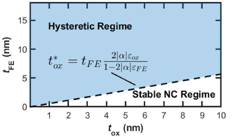
The constraint defined by (9) imposes a maximum allowed for a given (or vice-versa, a minimum for a given ), to achieve . This is visualized in Fig. 1, that shows the transition between hysteretic regime (i.e., ) and negative capacitance regime: (9) is in fact the opposite condition to that of stable negative-capacitance operation [14].
Note that to arrive at the simple approximate closed-form expression in (9), we assumed dominant inversion charge in the semiconductor that allowed considering the MOSFET capacitance to be equal to the oxide interlayer capacitance . In general however, the constraint as expressed in (9) is affected by the additional series capacitance provided by the semiconductor body of the underlying MOSFET [18], leading to a non-linear bias dependent .
2.3 Applicability Limits of the Modeling Approach
As specified in Section 1, the derivation of the analytical expressions (4)-(5), (6) was carried out starting from the Landau-Devonshire phenomenological theory (also known as ‘single-domain’ approximation) which treats ferroelectric as an homogeneous layer where, under the specific conditions discussed in Section 2.1, switching occurs between the two stable saturated polarization values [10]. In general, non-uniform polarization present in realistic ferroelectric thin layers can only be captured with the generalized Landau-Ginzburg theory that includes a domain interaction term in the expression of the free-energy [14]. However, recent attempts in the literature such as [19] demonstrate that it is possible to equivalently reproduce the effect of multi-domain interaction (which leads to gradual polarization switching) with multiple parallel single-domain models by considering finite ferroelectric switching time. In this work, we restricted the analysis to ’empirically’ reproduce of realistic FeFETs with effective , parameters that are able to capture the switching behavior of the saturated loops and neglecting the non-idealities that could reduce (i.e., counteracting trapping phenomena, wake-up of ferroelectric and other effects [4]).
Another important aspect related to ferroelectric HfO2 is the polycrystalline (i.e., amorphous) structure of realistic layers, which leads to fluctuations in properties of ferroelectric (such as the coercive field, ) [20]. Although beyond the scope of this work, we mention that the analytical model can be used to investigate the effect of variations, for example, by carrying out the derivation of (6) with respect to both , considering that with [15].
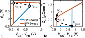
2.4 Non-Symmetric Switching Conditions
The lack of symmetry between and expressions is essentially caused by the non-linear and vs curves, see Fig. 2. At , see Fig. 2LABEL:sub@fig:r2_b, is equal to the critical value and this leads to a linear dependence of on as expressed by (5). Conversely, since , cannot be proportional to because this would require (if is positive then is negative, and vice-versa). could only occur in the accumulation region, for . In Section 2.5, we discuss possible strategies to maximize based on the optimization of switching conditions.
2.5 Guidelines to Maximize MW
The most obvious design strategy to increase is to increase , as reported in [22], where a -thick ferroelectric was employed to roughly double . However, this solution goes in contrast with the need of scaling the technology. With the aid of the analytical expressions derived in Section 2.1 it is possible to devise maximization strategies without compromising FeFET scaling.
As mentioned previously, the first strategy is based on the consideration that non-symmetric switching conditions reduce the maximum because is not proportional to . As also pointed out in [11], the theory predicts that another hysteresis loop can form between accumulation and depletion region that is basically symmetrical to the one from inversion to depletion (as the accumulation charge also depends exponentially on ). Thus, in principle, if a FeFET could switch from accumulation to inversion (and vice-versa), skipping the depletion region, then the switching conditions would become symmetrical and would consequently increase. To achieve this, the condition [with defined as in (4)] would have to be satisfied.
Another possible way to increase at the same and approaching the maximum theoretical limit [23, 24]:
| (10) |
is to engineer the insulator layer between the ferroelectric and the semiconductor. This goal can be achieved by either scaling or increasing (i.e., by employing high- insulators). In the limit, the oxide layer should be removed to maximize ; in fact, with then would increase of for and the ferroelectric parameters reported in Table 2.
3 Results
3.1 Geometrical and Universal Scaling of MW
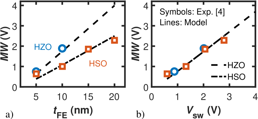
To verify the scaling trends of vs predicted by (6) we compared the analytical results with experimental data recently published in [4] of FeFETs realized with Zr- and Si- doped HfO2 (i.e., HZO and HSO) ferroelectrics. Fig. 3LABEL:sub@fig:r3_a shows the experimental vs data points (symbols) taken from [4] and the results obtained from (6) (lines). The ferroelectric parameters were set as follows: , and , , respectively. In both cases, was set to 16 [25]. With these sets of the calculated remnant polarization [15] is in the range of . These values are lower than the normally extracted for a MFM capacitor [4]. This discrepancy might be due to the fact that the ferroelectric in an MFIS structure normally operates in a subloop and that the polarization is lower than the maximum achievable by the ferroelectric itself (due to the lower field on the ferroelectric in the FeFET) [26].
Since (7), and , our model correctly anticipates the experimentally observed linear thickness-dependence of the . Equation (6) also suggests that regardless of the material and geometrical parameters, the should be only function of (on a first order approximation). Fig. 3LABEL:sub@fig:r3_b indeed reveals the universal trend of vs for different FE films. This important result comes from the fact that embeds the specific ferroelectric and geometric parameters and implies that regardless of the technology the scaling follows the same trend.
3.2 Assessing Endurance from MW Expression
As discussed in the Introduction, commercialization of FeFET has been hindered by the limited retention and endurance with respect to other technologies. Retention is defined as the time taken for the different states to be no longer distinguishable during a prolonged read operation. Instead, endurance is the time taken before states are indistinguishable after repeated program/erase operations. HfO2-based FeFETs have reduced trapping and lower depolarization over coercive field ratio with respect to PZT- or SBT-based devices leading to improved retention time [27]. However, endurance is still a major issue for this technology imposing an upper limit of writing cycles [28, 22] that is far from meeting the International Roadmap for Devices and Systems (IRDS) requirements of cycles [29]. At the basis of the limited endurance lies the increasing trapping due to the generation of oxide and interface states in the layer between the ferroelectric and the semiconductor body [30]. This is a consequence of the lower dielectric constant of SiO2 compared to that of doped-HfO2, that causes the local electric field to increase, accelerating generation of defects.
In the following, we derive an expression for the degraded during endurance tests. Fast decay due to depolarization fields and trapping/detrapping was not explicitly included in the model as it is expected to mainly influence retention rather than endurance [30, 27]. Our analysis focuses on both oxide and interface traps generation during these tests, in which the gate voltage is cycled with program and erase pulses to induce ferroelectric switching. The prolonged effect of high voltage pulses over time induces degradation in the form of generation of defects, and this is modeled with the analytical formula derived in Section 2 by adding the contribution due to the defects in the right-hand side of the SPE (1) [31]:
| (11) |
where is the generated trap concentration in the oxide interface layer (), is the generated interface trap density of states (), and is the body potential. These expressions assume that the charge neutrality level for the interface traps is located at Si mid-gap [31]. The stress causing generation of traps is induced by positive and negative pulses on the gate performing erase and program operations in the FeFET, respectively. Hence, will tend to decrease and to increase [21]. The concentration of generated defects during writing of the memory is in general different depending on the sign of the writing pulse, therefore the shifts in and will not be symmetric. Thus, we will use different symbols to indicate the generated defects during program and erase cycles, namely and for oxide and interface traps, respectively.
The degraded , , and expressions are derived by rewriting the threshold conditions, taking into account the additional potential drop due to defects expressed in (11) (the derivation is omitted for brevity). The ’s and degradation is expressed as follows:
| (12a) | ||||
| (12b) | ||||
| (12c) | ||||
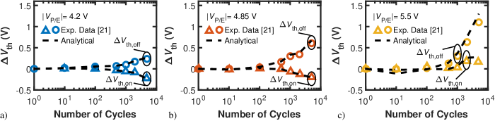
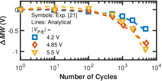
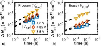
To assess the accuracy of the above expressions, we compared the analytical results with experimental data of endurance tests from [21]. The results in terms of and for three different values of program/erase pulse amplitude, are shown in Fig. 4 [ LABEL:sub@fig:r4_a, LABEL:sub@fig:r4_b, and LABEL:sub@fig:r4_c]. The , values set to match the experimental data trends are and , respectively. The duration of both program and erase pulse for each is , thus the time it takes for a single writing cycle is [21]. The combination of and degradation affects in turn, as shown in Fig. 5 for the same values of Fig. 4.
The trend of the degraded thresholds and is fully captured by and only. This happens because degradation primarily occurs in the insulator layer, as discussed previously. From this observation, simplified formula can be derived for , and . By neglecting variations in the modified SPE, (12a)-(12c) can be simplified as follows:
| (13a) | |||
| (13b) | |||
| (13c) | |||
Note that , , and are proportional to the variation introduced by the generation of both oxide and interface defects. The surface potential [corresponding to the logarithmic terms in square brackets in (13a)-(13b)] is calculated differently according to the two threshold conditions defined in Section 2.1. As intuition suggests, if the degradation were symmetric, i.e., the generated defects were giving equal and opposite in sign and , the variation would be .
The good agreement between analytical and experimental results in Figs. 4 and 5 was obtained by extracting the generated oxide and interface trap concentrations from and data in [21] following the approach described in [32]. That is, and were extracted by separating the threshold voltage shifts due to oxide () and interface traps () separately. The former is obtained from the mid-gap voltage, , that correlates with -induced drifts as at and , see (11); the latter is obtained by [21, 32]. To summarize, (12a)-(12c) transparently connect the FeFET parameters to the stress-dependent oxide and interface trap generation. As such, (12c) offers a powerful new -based characterization tool for extracting oxide and interface defects. This could serve either as an alternative to traditional techniques, or a stand-alone method to characterize defect densities under a variety of stress conditions. For instance, notice that when only generation affects degradation then it is possible to estimate the net generated traps from (13c):
| (14) |
This expression allows to simply and directly correlate measurements with generated traps. In the next section, we will exploit (14) to provide endurance predictions.
3.3 Writing Conditions Agnostic Endurance
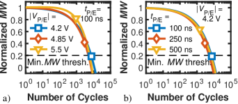
In the following we will show that the endurance extrapolated from the equations derived previously is not influenced by the writing conditions (in terms of and ). With the and data extracted in Section 3.2, it is possible to extrapolate the generated trap concentration for an arbitrary number of writing cycles. For simplicity and clarity of presentation, we will assume that the degradation is induced by oxide traps only (as supported by the experimental data in [21]) and neglect the generation of interface traps. The generated oxide trap density, is shown in Fig. 6LABEL:sub@fig:r6_a, LABEL:sub@fig:r6_b for both program and erase operation that set and , respectively. By fitting the experimental data in Fig. 6 it is found that generated oxide trap concentration follows a power law with respect to writing time (the duration of a single writing cycle being [21]):
| (15) |
where and are coefficients to fit experimental data, whose values for different writing conditions are collected in Table 1. Exponent in the range might be a signature of enhanced TDDB due to repeated cycling as reported in [33]. The extrapolated degradation obtained by using the predicted from the generation model is shown in Fig. 7LABEL:sub@fig:r7_a, LABEL:sub@fig:r7_b for different and values, respectively.
| Program (Vth,on) | Erase (Vth,off) | |||||
|---|---|---|---|---|---|---|
| () | () | () | ||||
| 4.2 | 0.45 | 0.25 | ||||
| 4.85 | 0.54 | 0.41 | ||||
| 5.5 | 0.54 | 0.41 | ||||
Note that values are normalized to the respective initial value for a fair comparison with different writing conditions. The FeFET is considered to fail to retain its memory operation after reaching the arbitrary minimum threshold set as the 20% of the initial value, see Fig. 7. Interestingly, from Fig. 7LABEL:sub@fig:r7_a it appears that increase does not degrade endurance significantly (at least for the range of values as in [21]). This is because higher leads to higher initial [4] but also higher , see Fig. 7. Similarly, Fig. 7LABEL:sub@fig:r7_b shows that increasing the pulse duration negligibly influences endurance. Note that in this case it was assumed that increase leads to the same increase in and initial to that caused by . This was done for the specific purpose of illustrating that if both and initial increase with program conditions, then the combined effect leads to negligible variation in endurance. Note that in general, if the assumption regarding and increase with (or ) is not satisfied, then the endurance limit will be affected by the writing conditions. The model can also predict the endurance improvement that can be obtained if the generated trap are decreased, either by improving the SiO2/Si interface quality or by reducing the field in the oxide layer. For example, if is decreased by one order of magnitude (and assuming every other parameter constant) then endurance can be extended to cycles. These considerations can be helpful to develop next generation FeFET with extended endurance.
4 Conclusions
In this paper, we derived an analytical expression of the Memory Window, , that can be used to investigate the scaling trends and endurance limits of FeFETs. Based on the Landau-Devonshire formalism, we arrived at closed-form expressions for the threshold voltages, , and for a conventional Metal-Ferroelectric-Insulator-Semiconductor (MFIS) structure that depends on critical technological and geometrical parameters. The expression also includes the effect of generated interface and oxide traps to assess the endurance limits of FeFETs. The key findings of this work are as follows:
-
1.
as expressed in (6) is a material-independent universal function of switching voltage, , embedding the dependence on critical design parameters.
-
2.
Constraints on minimum ferroelectric thickness () for a given oxide interface layer thickness (), see (9), impose a trade-off between scaling and amplitude.
-
3.
The being lower than the theoretical limit expressed in (10) is due to the non-symmetrical switching conditions.
- 4.
-
5.
can be used to extract oxide and interface trap concentration that are generated during endurance tests, see (14).
-
6.
The generated traps increase as a power-law, see (15), with time exponent . Under specific assumptions, the endurance limit is essentially independent of writing conditions.
5 Validation of the Analytical Model
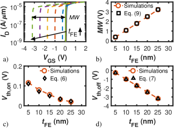
To verify the accuracy of the derived expression and of the underlying assumptions, we compared the analytical result of (4)-(5), (6) with numerical simulations. The comparison was done with simulations based on the Landau-Devonshire theory described in Section 2 to quantify the discrepancy with the analytical results. The simulations compute the self-consistent solution for from (1) coupled with the expression [34]. The Landau parameters are those used in Section 2.1 for the Si-doped HfO2 (i.e., HSO) (the full parameter set is collected in Table 2). The solution for and was then used to calculate the drain current via the Pao-Sah double integral [11, 34], see Fig. 8LABEL:sub@fig:r8_a from which the trend of with was extracted, as shown in Fig. 8LABEL:sub@fig:r8_b. Note that was chosen small enough to ensure hysteresis for the whole range considered (as discussed in Section 2.1). The agreement between the simulations and the analytical expressions, see Fig. 8, shows that the approximations made in the derivation of (4)-(6) are acceptable. Remarkably, the analytical expressions predict a weak decrease of with increasing , whereas decreases linearly, see Fig. 8LABEL:sub@fig:r8_c, LABEL:sub@fig:r8_d. This behavior follows from the consideration made in Section 2.4 on the non-symmetric switching, regarding the different conditions under which and are derived.
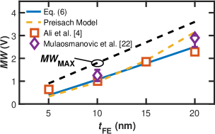
6 Comparison with Preisach Model
Ferroelectric switching behavior is described in the literature also by other models; here we focus on the Preisach model [16] which is broadly employed to interpret experimental results of FeFETs. In the framework of this model, the fact that measured is lower than the theoretical limit, see (10), is attributed to sub-hysteresis trajectories in the loop followed depending on the writing conditions [26, 23, 35]. The theoretical limit is thus not reached due to switching events with . In the case of the Landau formalism followed in this work, the same result of being lower than can be ascribed to non-symmetric switching conditions, as explained also in Section 2.4. This is supported by the comparison of the analytical results with numerical simulations carried out with a commercial software [36] on an MFIS structure with the Preisach model (the same parameter set was used, see Table 2). We performed numerical simulations with the Preisach model because, unlike with (6), it is not possible to derive a closed-form solution for the , because the switching points for the inner loops depend on the ferroelectric history and cannot be determined a priori. The comparison between the analytical expression derived in this work, the Preisach model and experimental data (from [4, 22]) shown in Fig. 9 confirms the fact that obtained both with Preisach and Landau model is below the theoretical limit .
7 Outline of the derivation of (12a)-(12b)
As mentioned in Section 3.2, the expressions for , , see (12a)-(12b), were derived by following the same procedure of Section 2.1 by modifying (1) as follows:
| (16) |
with the same symbols as previously defined. For , the expression for the charge at the switching condition () reads:
| (17) |
By substituting (17) and the corresponding (obtained as ) in (16), one obtaines (12a). For , the switching condition () does not alter and corresponding expressions. Thus, (12b) is simply obtained by substituting in (16). The expression for , see (12c), is obtained by subtracting (12b) from (12a).
Acknowledgment
The authors thank Thomas Mikolajick (NaMLab, TU Dresden), Francesco Maria Puglisi (University of Modena and Reggio Emilia), and Kamal Karda (Purdue University) for the valuable discussions.
References
- [1] J. L. Moll and Y. Tarui, “A New Solid State Memory Resistor,” IEEE Trans. on Electron Devices, vol. 10, no. 5, p. 338, Sep. 1963. 10.1109/T-ED.1963.15245
- [2] M. Okuyama, “Features, Principles and Development of Ferroelectric–Gate Field-Effect Transistors,” in Ferroelectric-Gate Field Effect Transistor Memories: Device Physics and Applications, 1st ed. Springer Netherlands, 2016, ch. 1, pp. 3–18. 10.1007/978-94-024-0841-6
- [3] S. Dünkel, M. Trentzsch, R. Richter, P. Moll, C. Fuchs, O. Gehring, M. Majer, S. Wittek, B. Müller, T. Melde, H. Mulaosmanovic, S. Slesazeck, S. Müller, J. Ocker, M. Noack, D. A. Löhr, P. Polakowski, J. Müller, T. Mikolajick, J. Höntschel, B. Rice, J. Pellerin, and S. Beyer, “A FeFET based super-low-power ultra-fast embedded NVM technology for 22nm FDSOI and beyond,” in IEDM Tech. Dig., Dec. 2017, pp. 19.7.1–19.7.4. 10.1109/IEDM.2017.8268425
- [4] T. Ali, P. Polakowski, S. Riedel, T. Büttner, T. Kämpfe, M. Rudolph, B. Pätzold, K. Seidel, D. Löhr, R. Hoffmann, M. Czernohorsky, K. Kühnel, X. Thrun, N. Hanisch, P. Steinke, J. Calvo, and J. Müller, “Silicon doped hafnium oxide (HSO) and hafnium zirconium oxide (HZO) based FeFET: A material relation to device physics,” Appl. Phys. Lett., vol. 112, no. 22, p. 222903, Jun. 2018. 10.1063/1.5029324
- [5] S. Salahuddin, K. Ni, and S. Datta, “The era of hyper-scaling in electronics,” Nat. Electron., vol. 1, no. 8, pp. 442–450, Aug. 2018. 10.1038/s41928-018-0117-x
- [6] X. Yin, A. Aziz, J. Nahas, S. Datta, S. Gupta, M. Niemier, and X. S. Hu, “Exploiting ferroelectric FETs for low-power non-volatile logic-in-memory circuits,” in Proc. IEEE/ACM Int. Conf. Comput.-Aided Design (ICCAD), Austin, TX, Nov. 2016, pp. 1–8. 10.1145/2966986.2967037
- [7] M. Jerry, P. Y. Chen, J. Zhang, P. Sharma, K. Ni, S. Yu, and S. Datta, “Ferroelectric FET analog synapse for acceleration of deep neural network training,” in IEDM Tech. Dig., vol. 6, Dic. 2017, pp. 6.2.1–6.2.4. 10.1109/IEDM.2017.8268338
- [8] A. Aziz, E. T. Breyer, A. Chen, X. Chen, S. Datta, S. K. Gupta, M. Hoffmann, X. S. Hu, A. Ionescu, M. Jerry, T. Mikolajick, H. Mulaosmanovic, K. Ni, M. Niemier, I. O’Connor, A. Saha, S. Slesazeck, S. K. Thirumala, and X. Yin, “Computing with ferroelectric FETs: Devices, models, systems, and applications,” in Proc. Design, Automat. Test Eur. Conf. Exhib, Mar. 2018, pp. 1289–1298. 10.23919/DATE.2018.8342213
- [9] J. Müller, T. S. Böscke, U. Schröder, S. Mueller, D. Bräuhaus, U. Böttger, L. Frey, and T. Mikolajick, “Ferroelectricity in simple binary ZrO2 and HfO2,” Nano Lett., vol. 12, no. 8, pp. 4318–4323, 2012. 10.1021/nl302049k
- [10] S. Salahuddin and S. Datta, “Use of negative capacitance to provide voltage amplification for low power nanoscale devices,” Nano Lett., vol. 8, no. 2, pp. 405–410, 2008. 10.1021/NL071804G
- [11] H. P. Chen, V. C. Lee, A. Ohoka, J. Xiang, and Y. Taur, “Modeling and design of ferroelectric MOSFETs,” IEEE Trans. on Electron Devices, vol. 58, no. 8, pp. 2401–2405, Aug. 2011. 10.1109/TED.2011.2155067
- [12] G. Pahwa, T. Dutta, A. Agarwal, and Y. S. Chauhan, “Physical Insights on Negative Capacitance Transistors in Nonhysteresis and Hysteresis Regimes: MFMIS Versus MFIS Structures,” IEEE Trans. on Electron Devices, vol. 65, no. 3, pp. 867–873, Mar. 2018. 10.1109/TED.2018.2794499
- [13] N. Zagni, P. Pavan, and M. A. Alam, “Two-dimensional MoS2 negative capacitor transistors for enhanced (super-Nernstian) signal-to-noise performance of next-generation nano biosensors,” Appl. Phys. Lett., vol. 114, no. 23, p. 233102, Jun. 2019. 10.1063/1.5097828
- [14] M. Hoffmann, M. Pešić, S. Slesazeck, U. Schroeder, and T. Mikolajick, “On the stabilization of ferroelectric negative capacitance in nanoscale devices,” Nanoscale, vol. 10, no. 23, pp. 10 891–10 899, 2018. 10.1039/c8nr02752h
- [15] G. Pahwa, T. Dutta, A. Agarwal, and Y. S. Chauhan, “Compact model for ferroelectric negative capacitance transistor with MFIS structure,” IEEE Trans. on Electron Devices, vol. 64, no. 3, pp. 1366–1374, Mar. 2017. 10.1109/TED.2017.2654066
- [16] M. A. Alam, M. Si, and P. D. Ye, “A critical review of recent progress on negative capacitance field-effect transistors,” Appl. Phys. Lett., vol. 114, no. 9, p. 090401, Mar. 2019. 10.1063/1.5092684
- [17] A. Rusu, A. Saeidi, and A. M. Ionescu, “Condition for the negative capacitance effect in metal-ferroelectric-insulator-semiconductor devices,” Nanotechnology, vol. 27, no. 11, p. 115201, 2016. 10.1088/0957-4484/27/11/115201
- [18] W. Cao and K. Banerjee, “Is negative capacitance FET a steep-slope logic switch?” Nature Communications, vol. 11, no. 1, pp. 1–8, dec 2020. 10.1038/s41467-019-13797-9
- [19] J. Gomez, S. Dutta, K. Ni, J. Smith, B. Grisafe, A. Khan, and S. Datta, “Hysteresis-free negative capacitance in the multi-domain scenario for logic applications,” in IEDM Tech. Dig. San Francisco, CA, USA: IEEE, Dec. 2019, pp. 7.1.1–7.1.4. 10.1109/IEDM19573.2019.8993638
- [20] K. Chatterjee, S. Kim, G. Karbasian, D. Kwon, A. J. Tan, A. K. Yadav, C. R. Serrao, C. Hu, and S. Salahuddin, “Challenges to Partial Switching of Hf0.8Zr0.2O2 Gated Ferroelectric FET for Multilevel/Analog or Low Voltage Memory Operation,” IEEE Electron Device Lett., vol. 40, no. 9, pp. 1–1, Sep. 2019. 10.1109/led.2019.2931430
- [21] B. Zeng, M. Liao, J. Liao, W. Xiao, Q. Peng, S. Zheng, and Y. Zhou, “Program/Erase Cycling Degradation Mechanism of HfO 2 -Based FeFET Memory Devices,” IEEE Electron Device Lett., vol. 40, no. 5, pp. 710–713, May 2019. 10.1109/LED.2019.2908084
- [22] H. Mulaosmanovic, E. T. Breyer, T. Mikolajick, and S. Slesazeck, “Ferroelectric FETs With 20-nm-Thick HfO 2 Layer for Large Memory Window and High Performance,” IEEE Trans. on Electron Devices, vol. 66, no. 9, pp. 3828–3833, Sep. 2019. 10.1109/TED.2019.2930749
- [23] H. T. Lue, C. J. Wu, and T. Y. Tseng, “Device modeling of ferroelectric memory field-effect transistor (FeMFET),” IEEE Trans. on Electron Devices, vol. 49, no. 10, pp. 1790–1798, Oct. 2002. 10.1109/TED.2002.803626
- [24] J. M. Sallese and V. Meyer, “The ferroelectric MOSFET: A self-consistent quasi-static model and its implications,” IEEE Trans. on Electron Devices, vol. 51, no. 12, pp. 2145–2153, Dec. 2004. 10.1109/TED.2004.839113
- [25] M. Y. Kao, A. B. Sachid, Y. K. Lin, Y. H. Liao, H. Agarwal, P. Kushwaha, J. P. Duarte, H. L. Chang, S. Salahuddin, and C. Hu, “Variation Caused by Spatial Distribution of Dielectric and Ferroelectric Grains in a Negative Capacitance Field-Effect Transistor,” IEEE Trans. on Electron Devices, vol. 65, no. 10, pp. 4652–4658, Oct. 2018. 10.1109/TED.2018.2864971
- [26] K. Ni, P. Sharma, J. Zhang, M. Jerry, J. A. Smith, K. Tapily, R. Clark, S. Mahapatra, and S. Datta, “Critical Role of Interlayer in Hf 0.5 Zr 0.5 O 2 Ferroelectric FET Nonvolatile Memory Performance,” IEEE Trans. on Electron Devices, vol. 65, no. 6, pp. 2461–2469, Jun. 2018. 10.1109/TED.2018.2829122
- [27] N. Gong and T. P. Ma, “Why Is FE-HfO2 More Suitable Than PZT or SBT for Scaled Nonvolatile 1-T Memory Cell? A Retention Perspective,” IEEE Electron Device Lett., vol. 37, no. 9, pp. 1123–1126, Sep. 2016. 10.1109/LED.2016.2593627
- [28] E. Yurchuk, J. Muller, J. Paul, T. Schlosser, D. Martin, R. Hoffmann, S. Mueller, S. Slesazeck, U. Schroeder, R. Boschke, R. Van Bentum, and T. Mikolajick, “Impact of scaling on the performance of HfO2-based ferroelectric field effect transistors,” IEEE Trans. on Electron Devices, vol. 61, no. 11, pp. 3699–3706, Nov. 2014. 10.1109/TED.2014.2354833
- [29] “IEEE International Roadmap for Devices and Systems - Beyond CMOS,” 2018. [Online]. Available: https://irds.ieee.org/editions/2018/beyond-cmos
- [30] E. Yurchuk, S. Mueller, D. Martin, S. Slesazeck, U. Schroeder, T. Mikolajick, J. Muller, J. Paul, R. Hoffmann, J. Sundqvist, T. Schlosser, R. Boschke, R. Van Bentum, and M. Trentzsch, “Origin of the endurance degradation in the novel HfO2-based 1T ferroelectric non-volatile memories,” in Proc. IEEE Int. Rel. Phys. Symp., Waikoloa, HI, USA, 2014, pp. 2E.5.1–2E.5.5. 10.1109/IRPS.2014.6860603
- [31] I. S. Esqueda and H. J. Barnaby, “A defect-based compact modeling approach for the reliability of CMOS devices and integrated circuits,” Solid-State Electron., vol. 91, pp. 81–86, Jan. 2014. 10.1016/J.SSE.2013.10.008
- [32] D. K. Schroder, “Oxide and Interface Trapped Charges, Oxide Thickness,” in Semiconductor Material and Device Characterization, 3rd ed. John Wiley & Sons, Inc., 2005, ch. 6, pp. 319–387. 10.1002/0471749095
- [33] A. Kerber, A. Vayshenker, D. Lipp, T. Nigam, and E. Cartier, “Impact of charge trapping on the voltage acceleration of TDDB in metal gate/high-k n-channel MOSFETs,” in Proc. IEEE Int. Rel. Phys. Symp., Anaheim, CA, USA, May 2010, pp. 369–372. 10.1109/IRPS.2010.5488803
- [34] Y. Taur and T. H. Ning, Fundamentals of Modern VLSI Devices, 2nd ed. Cambridge University Press, 2009.
- [35] B. Jiang, P. Zurcher, R. E. Jones, S. J. Gillespie, and J. C. Lee, “Computationally efficient ferroelectric capacitor model for circuit simulation,” in Proc. IEEE VLSI Technol.,, Jun. 1997, pp. 141–142. 10.1109/VLSIT.1997.623738
- [36] Synopsys, “Sentaurus SDevice Manual (O-2018.06),” 2018.