Dispersion tailoring in wedge microcavities for Kerr comb generation
Abstract
The shaping of group velocity dispersion in microresonators is an important component in the generation of wideband optical frequency combs. Small resonators – with tight bending radii – offer the large free-spectral range desirable for wide comb formation. However, the tighter bending usually limit comb formation as it enhances normal group velocity dispersion. We experimentally demonstrate that engineering the sidewall angle of small-radius ( m), 3 m-thick silica wedge microdisks enables dispersion tuning in both normal and anomalous regimes, without significantly affecting the free spectral range. A microdisk with wedge angle of (anomalous dispersion) is used to demonstrate a 300 nm bandwidth Kerr optical frequency comb.
The generation and control of Kerr optical frequency combs in microcavities are fundamental steps towards broadband on-chip coherent light sources Gaeta et al. (2019). These sources have been successfully employed in optical communications Marin-Palomo et al. (2017) , frequency metrology Papp et al. (2014), spectroscopy Dutt et al. (2018), and range measurement Suh and Vahala (2018). Many of these applications often benefit from the dissipative cavity soliton (CS) regime observed in the anomalous optical group velocity dispersion (GVD) spectral region Gaeta et al. (2019). Mid-infrared light sources based on parametric oscillation also explores dispersion Sayson et al. (2019) control in the normal GVD regime. Either way, harnessing the properties of microcombs demands for microcavity alternatives with tailorable GVD. Silica wedge microcavities offer a versatile solution for on-chip comb-generation due to its potentially ultra-high optical quality factors () Lee et al. (2012) and simple fabrication process. In this type of optical microcavity, illustrated in Fig. 1(a), a shallow wedge is obtained by an isotropic wet etch of the silica glass that not only ensures a smooth glass-air boundary but also reduces the optical-field overlap with the etched glass surface Lee et al. (2012). However, the geometrical effect of the wedge on the GVD is to enhance normal dispersion. As a result, shallow-wedge cavities only exhibit anomalous dispersion at sufficiently large radii, when the wedge-induced GVD is counteracted by silica’s anomalous dispersion. Indeed, effective control of zero GVD wavelength in such large radii cavities has been achieved using two-angle wedges Yang et al. (2016) around the 1550 nm telecom band, though it requires a fine control over a nontrivial two-step wet etching. Closer to visible wavelengths, effective GVD control in silica resonators and consequent frequency comb generation has also been achieved using avoided mode crossing Lee et al. (2017) or large wedge angles Li et al. (2015); Ma et al. (2019) achieved using a dry plasma etching. Although large cavities are advantageous for many frequency comb applications that require GHz-range linespacing Marin-Palomo et al. (2017); Dutt et al. (2018), they usually suffer from small bandwidth due to a universal scaling law (, is the comb bandwidth and is the cavity radius) Coen and Erkintalo (2013). Therefore, smaller cavities with large free spectral range (FSR) are often desirable when targeting at full octave frequency combs Okawachi et al. (2011); Pfeiffer et al. (2017); Li et al. (2017).
Here we demonstrate that either anomalous or normal GVD can be achieved at telecom wavelength using small radius (100 µm) silica wedge cavities. Our approach explores strong photoresist adhesion in a wet etching process that enables unusually large wedge angles. Using this GVD control approach we demonstrate anomalous dispersion frequency comb formation in a broad pump wavelength range. Furthermore, by tuning the tapered fiber bus waveguide diameter we obtain a clean transmission spectrum Nasir et al. (2016) that allows for optical mode identification and direct measurement of GVD.
Group-velocity dispersion is strongly influenced by both material and geometric (modal) dispersion. In optical cavities with bent sections, the optical angular momentum around curves localize higher frequency waves towards the cavity outer edges, effectively increasing the round-trip time and decreasing the mode FSR, contributing to a normal-GVD. Although such normal-GVD contribution can be overcome by cross-section engineering within ring resonators Razzari et al. (2009); Pfeiffer et al. (2017); Li et al. (2017), disk cavities offer less degrees of freedom to suppress the normal dispersion contribution. In wedge-shaped microdisk the normal-GVD is further amplified: higher frequency modes (shorter wavelengths) penetrate deeper in the outer wedge tip, further reducing their FSR when compared to longer wavelength modes. Despite silica’s anomalous material GVD at telecom wavelengths, this curvature effect is so strong that it can ultimately prevent anomalous GVD within small radii wedge resonators.
In optical microcavities it is more meaningful to represent GVD by inspecting how the frequency separation between two adjacent longitudinal optical modes – the Free Spectral Range (FSR) – changes along the spectrum. The frequency dependence of the FSR can be expressed by series expansion of optical frequency around a given reference mode,
| (1) |
where is an integer label for the mode (relative to a reference mode ) and is a reference mode frequency. As for the coefficients, corresponds to the FSR, to its variation rate with , and so forth. Since the FSR of a cavity is given by ( being the group velocity and the cavity’s length), anomalous GVD () corresponds to a positive .
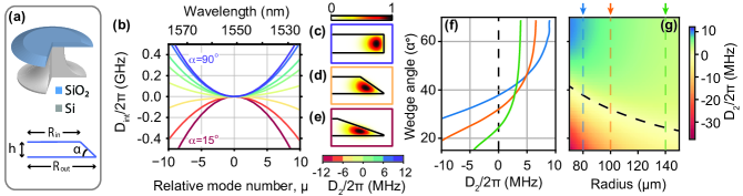
The qualitative arguments given above regarding the GVD are confirmed when we analyze the wedge microdisk cavity through numerical simulations. As far as mode polarization is concerned, we follow the convention used in Lee et al. (2012) where the TM (transverse magnetic) mode is the one whose transverse electric field is roughly oriented along the bottom flat oxide-air surface. In the following discussion we will always be referring to the TE (transverse electric) mode, as it usually has the highest quality factor due to its lower overlap with the wedge surface. Figure 1(b) presents the simulated residual dispersion, highlighting the GVD contribution in Eq. 1 for the fundamental mode of a small radius thin wedge cavity (m thick and µm). as the wedge angles varies from ( µm) to ( µm). Figures 1(c-e) show the effect of the wedge angle in the total electric field distribution – the wedge shape can concentrate short-wavelength modes towards its tip. The interplay between the wedge-induced dispersion and cavity curvature is quantified in Fig.1(f): at shorter radii, larger wedge angles are required to achieve zero GVD. In Fig.1(g) we show a full map of the GVD (represented by ) when both radius and wedge angle are varied, the zero-GVD loci confirms that large angles are necessary to balance the curvature-induced GVD contribution.
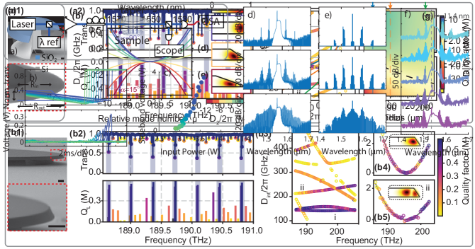
In order to fabricate both shallow and steep wedge resonators we employed a technique devised in Lee et al. (2012), starting with a µm SiO2 layer grown by wet oxidation over a silicon substrate. As previously reported Lee et al. (2012), shallow angles result from the gradual peeling of the resist pads, caused by infiltration of the etchant between the photoresist and the silica layer. The uniformity of the wedge surface is a consequence of the prolonged isotropic etching, combined with the moderate adhesion of the resist to the substrate. This is what renders achieving large wedge angles a challenging task when using resist soft masks; for instance, the largest angles reported in Lee et al. (2012) are 27∘, while hard-mask (Cr) process has been used to achieve almost wedge-free disks (although with rather low quality factor) Long et al. (2017). To ensure a uniform peeling rate, we employed photoresist (Shipley sc-1827) to fabricate the shallow wedges, while large angle resonators were obtained by using MaN-2405 electron resist that has strong adhesion. In both cases, resist adhesion was improved using surfactant SURPASS 3000 and resist reflow (temperature of C for sc-1827 and C for MaN-2405, both for 5 min). The electron resist was exposed with an electron beam, but it can also be exposed using deep UV light. The silicon undercut was performed using a TMAH (Tetra-Methyl-Amonium Hydroxide) wet etch, which results in an anisotropic pedestal. The fabricated devices are shown in Fig. 2(a1,b1). Using an atomic force microscope, we determine the wedge angles to be approximately and .
The GVD and the optical quality factor of the devices were obtained from the transmission spectra, which were measured by bringing a straight tapered fiber in contact with the microcavity. The transmitted signal from a tunable external cavity laser (Yenista Tunics Reference SCL) was detected with a 1 GHz bandwidth photodetector (New Focus 1623) and recorded by a real-time oscilloscope (Agilent DSO9023A, 2 GHz, 20 Msamples). For the purpose of dispersion measurement, it is of uttermost importance to have a precise frequency calibration for the scanning laser, which was obtained by simultaneously monitoring the transmission of a fiber-based (Corning SMF28) Mach-Zehnder interferometer (calibrated with =137(10) MHz, Hz) and an acetylene gas cell. We also verified that the laser scanning speed (10 nm/s) was not limiting our quality factor measurements by comparing them with narrow-band measurements obtained with piezo-scanning of the laser frequency. The fundamental optical mode is thus isolated by employing thicker tapers ( µm) that decrease the phase-matching between the taper optical mode and the higher order disk modes Nasir et al. (2016). Using the full bandwidth of our laser (1460 - 1610 nm), we measured the fundamental TE mode loaded quality factor () to be around for the steep wedges, and for the shallow wedges, as shown in Figs. 2(a2) and 2(b2). Scanning electron microscope (SEM) images of the devices (shown in figures 2(a1) and (b1)) suggest that this discrepancy is due to lithography-related sidewall roughness rather than the actual wedge angles.
A general picture of the GVD in our devices can be obtained by inspecting Fig. 2 (a3, b3). These curves are obtained in three steps: (i) we assign a single relative azimuthal number to all modes lying within one FSR in the measured transmission, Figs. 2( a2, b2). Their resonant frequencies are then (ii) plotted against the azimuthal numbers; a straight line fitted to this data corresponds to an average FSR () of the measured cavity modes. Next, (iii) an overall picture of the GVD () for all modes around is obtained by subtracting () from the dataset, where corresponds to the inspection frequency . For example, in Figs. 2(a3, b3) the chosen inspection frequency is THz ( nm) and the subtracted linear trend corresponds to an average FSRs of GHz ( nm). The significant difference in slopes noticeable in Figs. 2(a3, b3) reflects the distinct FSRs of each modal family. Avoided mode crossings within higher order modes can be easily identified in this representation. From Figs. 2(a3, b3) we can slice specific optical mode branches from the dataset and fit Eq. 1 to them. In this last step, the precise values for of the chosen branch are calculated In Figs. 2(a4, a5, b4, b5) we show the fitted model of Eq. 1 for two modes mode branches with highest of each device. As expected from Eq. 1, the residual dispersion for each mode family appear as parabola-shaped curves centered at the inspection frequency. In the small-angle wedge () of Fig. 2(a4, a5) we obtain normal GVD; whereas anomalous GVD is obtained for the large-angle wedge. We identify these modes as the first two lowest order optical modes by comparing their measured and ) with numerical simulations.
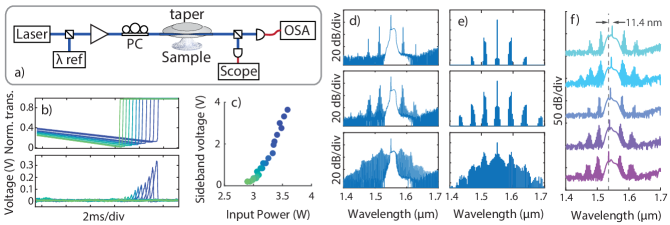
Using the anomalous GVD engineered resonator, we were able to consistently generate optical frequency combs by pumping the resonator at the optical mode shown in Fig. 2(b4). Figure 3(a) outlines the experimental setup used for comb generation: the amplitude of the CW Tunics laser is modulated by an EOM (electro-optical modulator) and then amplified with an EDFA (erbium doped fiber amplifier), concentrating up to 14 W (peak power) into 40 ns pulses (1 MHz repetition rate). The pulse duration is long enough to ensure a quasi-CW regime. The cavity transmission is analyzed with an oscilloscope and an OSA (optical spectrum analyzer).
Choosing a resonance at approximately 1550 nm, we determined the threshold power for comb generation and studied its formation dynamics. The threshold was measured by simultaneously monitoring the pump transmission and the power of the first generated sideband while scanning the laser frequency with a piezo-actuator. The sideband power was measured by the OSA centered at 1527 nm with zero span and resolution bandwidth of 2 nm, resulting a voltage signal proportional to its power. The results are presented in Fig. 3(b), where the color scale shifts from green to blue as input power increases. We notice that the first comb sidebands are generated towards the end of the bistable transmission and its intensity diminishes as the resonance minimum is blue-shifted at smaller input powers. The sideband maximum power evolution (Fig. 3(c)), allows us to identify the threshold near 2.9 W, which is in reasonable agreement with the predicted threshold for comb generation (2 W for an effective mode area µm2) ) Herr et al. (2012).
For the comb formation measurements, we captured the OSA spectra as the laser (14 W input peak power) is tuned towards the bistable resonance in 1 pm steps. Figure 3(d) highlights the different formation stages: at first, primary sidebands are generated 13 FSRs away from each other. Then, secondary sidebands rise around the primary lines in adjacent modes, until the sub-combs merge into a single broader comb, as expected for small FSR devices Herr et al. (2012). The coupled mode equations for the entire system were solved with the open-source CombGUI toolbox, and the simulation results based on the measured experimental parameters are in good agreement with the experimental data, as shown in Fig. 3e). Finally, since our modal dispersion engineering does not rely on avoided crossings Kim et al. (2017), combs could be excited at every FSR step of the pump laser. Fig. 3(f) shows some example combs generated within an 11 nm range (4 FSRs) around 1550 nm.
In conclusion, we demonstrate that small radii wedge resonators can be engineered to enable either normal or anomalous GVD. Since our approach does not rely on avoided crossings, not only it allows for comb excitation in a broad range of pump frequencies but also may be more easily explored towards octave spanning frequency combs. Our GVD engineering strategy, if combined with disk thickness control, could also be extended towards other frequency ranges or wedge materials Ramiro-Manzano et al. (2012); Kang et al. (2017) . Extension of our results may allow the control of higher order GVD (e.g. ) and enable phase-matching at exotic wavelengths.
Funding: this work was funded by FAPESP (2012/17610-3, 2012/17765-7, 2016/05038-4, 2018/15577-5, 2018/21311-8, 2018/15580-6, 2018/25339-4), Coordenação de Aperfeiçoamento de Pessoal de Nível Superior - Brasil (CAPES) (Finance Code 001), and CNPq. Acknowledgements: we acknowledge Antônio Von Zuben for his support in the microfabrication, and Center for Semiconductor Components and Nanotechnologies and MultiUser Laboratory (LAMULT) for providing the micro-fabrication infrastructure. Disclosure: the authors declare no conflicts of interest.
References
- Gaeta et al. (2019) A. L. Gaeta, M. Lipson, and T. J. Kippenberg, Nature Photonics 13, 158 (2019).
- Marin-Palomo et al. (2017) P. Marin-Palomo, J. N. Kemal, M. Karpov, A. Kordts, J. Pfeifle, M. H. P. Pfeiffer, P. Trocha, S. Wolf, V. Brasch, M. H. Anderson, R. Rosenberger, K. Vijayan, W. Freude, T. J. Kippenberg, and C. Koos, Nature 546, 274 (2017).
- Papp et al. (2014) S. B. Papp, K. Beha, P. Del’Haye, F. Quinlan, H. Lee, K. J. Vahala, and S. A. Diddams, Optica 1, 10 (2014).
- Dutt et al. (2018) A. Dutt, C. Joshi, X. Ji, J. Cardenas, Y. Okawachi, K. Luke, A. L. Gaeta, and M. Lipson, Science Advances 4, e1701858 (2018).
- Suh and Vahala (2018) M.-G. Suh and K. J. Vahala, Science 359, 884 LP (2018).
- Sayson et al. (2019) N. L. B. Sayson, T. Bi, V. Ng, H. Pham, L. S. Trainor, H. G. L. Schwefel, S. Coen, M. Erkintalo, and S. G. Murdoch, Nature Photonics 13, 701–706 (2019).
- Lee et al. (2012) H. Lee, T. Chen, J. Li, K. Y. Yang, S. Jeon, O. Painter, and K. J. Vahala, Nature Photonics 6, 369 (2012).
- Yang et al. (2016) K. Y. Yang, K. Beha, D. C. Cole, X. Yi, P. Del’Haye, H. Lee, J. Li, D. Y. Oh, S. A. Diddams, S. B. Papp, and K. J. Vahala, Nature Photonics 10, 316 (2016).
- Lee et al. (2017) S. H. Lee, D. Y. Oh, Q.-F. Yang, B. Shen, H. Wang, K. Y. Yang, Y.-H. Lai, X. Yi, X. Li, and K. Vahala, Nature Communications 8, 1295 (2017).
- Li et al. (2015) G. Li, P. Liu, X. Jiang, C. Yang, J. Ma, H. Wu, and M. Xiao, Photon. Res. 3, 279 (2015).
- Ma et al. (2019) J. Ma, L. Xiao, J. Gu, H. Li, X. Cheng, G. He, X. Jiang, and M. Xiao, Photonics Research 7, 573 (2019).
- Coen and Erkintalo (2013) S. Coen and M. Erkintalo, Optics Letters 38, 1790 (2013).
- Okawachi et al. (2011) Y. Okawachi, K. Saha, J. S. Levy, Y. H. Wen, M. Lipson, and A. L. Gaeta, Optics Letters 36, 3398 (2011).
- Pfeiffer et al. (2017) M. H. P. Pfeiffer, C. Herkommer, J. Liu, H. Guo, M. Karpov, E. Lucas, M. Zervas, and T. J. Kippenberg, Optica 4, 684 (2017).
- Li et al. (2017) Q. Li, T. C. Briles, D. A. Westly, T. E. Drake, J. R. Stone, B. R. Ilic, S. A. Diddams, S. B. Papp, and K. Srinivasan, Optica 4, 193 (2017).
- Nasir et al. (2016) M. N. M. Nasir, G. S. Murugan, and M. N. Zervas, J. Opt. Soc. Am. B 33, 1963 (2016).
- Razzari et al. (2009) L. Razzari, D. Duchesne, M. Ferrera, R. Morandotti, S. Chu, B. E. Little, and D. J. Moss, Nature Photonics 4, 41 (2009).
- Long et al. (2017) H. Long, W. Yang, L. Y. Ying, and B. P. Zhang, Chinese Phys. B 26, 54211 (2017).
- Herr et al. (2012) T. Herr, K. Hartinger, J. Riemensberger, C. Y. Wang, E. Gavartin, R. Holzwarth, M. L. Gorodetsky, and T. J. Kippenberg, Nature Publishing Group 6, 480 (2012).
- Kim et al. (2017) S. Kim, K. Han, C. Wang, J. A. Jaramillo-Villegas, X. Xue, C. Bao, Y. Xuan, D. E. Leaird, A. M. Weiner, and M. Qi, Nature Communications 8, 372 (2017).
- Ramiro-Manzano et al. (2012) F. Ramiro-Manzano, N. Prtljaga, L. Pavesi, G. Pucker, and M. Ghulinyan, Optics Express 20, 22934 (2012).
- Kang et al. (2017) G. Kang, M. R. Krogstad, M. Grayson, D.-G. Kim, H. Lee, J. T. Gopinath, and W. Park, Optics Express 25, 15581 (2017).