Fast tunable high Q-factor superconducting microwave resonators
Abstract
We present fast tunable superconducting microwave resonators fabricated from planar NbN on a sapphire substrate. The wavelength resonators are tuning fork shaped and tuned by passing a dc current which controls the kinetic inductance of the tuning fork prongs. The section from the open end operates as an integrated impedance converter which creates a nearly perfect short for microwave currents at the dc terminal coupling points, thus preventing microwave energy leakage through the dc lines. We measure an internal quality factor over the entire tuning range. We demonstrate a tuning range of and tuning response times as short as 20 ns for the maximum achievable detuning. Due to the quasi-fractal design, the resonators are resilient to magnetic fields of up to 0.5 T.
I Introduction
Superconducting microwave resonators are versatile devices with applications ranging from signal conditioning in Purcell filters Reed et al. (2010) and parametric amplifiers Wustmann and Shumeiko (2013); Simoen et al. (2015) to sensing applications such as kinetic inductance detectors Day et al. (2003) and near field scanning microwave microscopes de Graaf et al. (2013); De Graaf et al. (2015); Geaney et al. (2019). In particular, in the rapidly developing field of quantum computing superconducting resonators are used for qubit readout, on demand storage/release Pierre et al. (2014) and routing of single microwave photons Yin et al. (2013); Hoi et al. (2011), and deployed as qubit communication buses Wendin (2017). Furthermore, future progress in quantum computing calls for identification and elimination of material defects, which spoil coherence in quantum circuits Paladino et al. (2014); Müller et al. (2019). This urgent need stimulated the development of planar Electron Spin Resonance (ESR) spectrometers with sub-femtomole sensitivity de Graaf et al. (2017); De Graaf et al. (2018) to environmental spins. The frequency tuning functionality either greatly benefits (filters, sensors, spectrometers) or is instrumental for (parametric amplifiers, single photon sources) all the above applications.
The base frequency of any microwave resonator is defined by its geometry and can therefore be adjusted by varying the geometrical parameters. In practice, purely mechanical designs are bulky, challenging to implement Kim et al. (2011) and do not provide fast tuning.
Conveniently, superconducting design elements provide an alternative option: any superconductor possesses kinetic inductance (KI), which can be tuned with either external magnetic field or dc bias current. The first approach does not require any tweaks to a standard coplanar resonator design and was presented already a decade ago by Healey et al. Healey et al. (2008). However, sweeping the external magnetic field is also a rather slow solution; the kinetic inductance itself can respond in sub-nanosecond time (the instantaneous KI response is, for example, exploited in traveling wave parametric amplifiers Eom et al. (2012); Chaudhuri et al. (2017) and comb generators Erickson et al. (2014)).
A standard way to achieve fast frequency control via KI tuning is by integrating a pair of Josephson junction elements in the form of a Superconducting Quantum Interference Device (SQUID) loop in the resonator design. The highly nonlinear loop inductance can be controlled with a magnetic flux generated by a dedicated current control line, such that no external field is needed. Devices of this type achieve tuning speeds faster than the photon lifetime Sandberg et al. (2008), and recently a frequency tuning time less than ns was demonstrated Wang et al. (2013). Today, SQUID-tunable resonators have become a common element in circuit QED experiments Palacios-Laloy et al. (2008); Osborn et al. (2007); Kennedy et al. (2019). Unfortunately, the insertion of Josephson elements degrades the resonance quality: first designs demonstrated , and in best-ever devices still does not exceed 35000 Svensson et al. (2018). This is significantly lower than standard non-tunable coplanar resonators, where is now typical Megrant et al. (2012).
As an alternative to SQUIDs as lumped KI elements, one can exploit the kinetic inductance of the superconducting film itself. This approach does not introduce the extra internal dissipation associated with SQUIDs, but generally does increase radiation losses: the microwave energy leaks from the cavity through the dc terminals. An obvious way to minimize the losses is to couple the dc leads at the nodes of the microwave voltage, but, due to fabrication tolerances, one does not reach in a practical device. The leakage can be further suppressed by supplying the bias current through low pass filters. The simplest of such filters, capacitors, provide a shunt to ground for microwaves, thus effectively decouplindg dc lines. With this design, internal quality factors up to in tunable coplanar resonators were demonstrated in Bosman et al. (2015). The maximum is limited by two factors: the filter capacitor cannot be made larger than few tens of pF because of self-resonances, and the capacitor is non-ideal because of the finite loss tangent of the dielectric layer. The dielectric losses were the the limiting factor in Bosman et al. (2015). With a better dielectric such as aluminium oxide deposited by atomic layer deposition (ALD), factors up to in tunable microstrip resonators have been reached Adamyan et al. (2016). Another simple filter type, an inductive-resistive (LR) filter, was reported in Vissers et al. (2015). With the choke inductance nH and resistance , -factors up to were reported. However, this solution involves the trade-off between the quality factor and the maximum tuning rate: the is limited by the losses in the dissipative , therefore has to be kept small, and a high is needed to effectively isolate ; both requirements slow down the response time ns. If few-nanosecond tuning time is required, the achievable -factor would not exceed that of SQUID-tunable resonators.
Here, we present a novel resonator design which incorporates an impedance converter as an integral part of the resonator circuit. The converter provides a nearly perfect short circuit for microwave currents at the dc terminals insertion points thus preventing an energy leakage into terminals. By design, this solution imposes no limits on the frequency tuning rate and we report dissipative -factors above one million at high photon populations and up to at single photon level, approaching that of standard non-tunable superconducting coplanar resonators.
II Methods
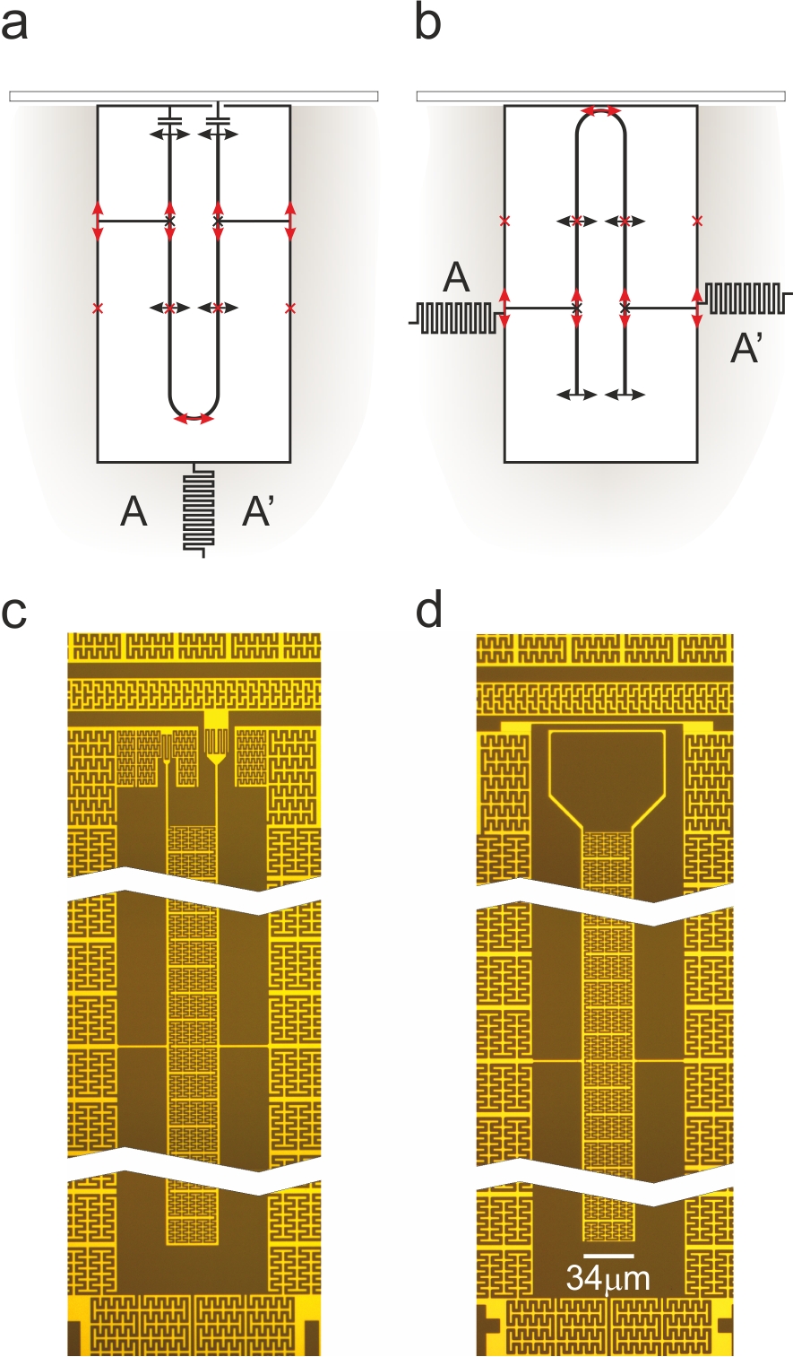
The resonator design is sketched in Fig. 1(a, b). Conceptually, the resonator core is an electromagnetic analog of the mechanical tuning fork. The coupling to a readout coplanar waveguide transmission line is provided either via an interdigitaited capacitor (a) or by an inductive loop (b). As it will be demonstrated below, the resulting device performance does not depend on the coupling scheme, so any solution can be freely chosen for a specific target application. The detailed design can be seen in optical images presented in Fig. 1(c, d): the two tuning fork prongs are designed to be 2 m in width. The prongs are inductive elements which are coupled via an interdigitated capacitor formed by a 3rd order quasi-fractal pattern. The role of the quasi-fractal design will be discussed in detail below; in summary it is a descendent of non-tunable resonators presented earlier in de Graaf et al. (2012, 2014).
We exploit the mode of the tuning fork. The current/voltage nodes/antinodes of this mode are depicted in Figs. 1(a,b): the mode supports a voltage node at a distance of away from the open end of the resonator. This is the point on the prongs where we inject a dc current via a galvanic connection to the ground plane. The bias current thus flows along the closed U-turn section of the fork and controls the kinetic inductance of the resonator’s section, allowing the resonance frequency to be tuned. To allow for the dc bias, the ground plane is split into two sections A and A’, galvanically separated by a large interdigitated capacitor(s) (sketched as meander(s) in Fig. 1(a, b)), that present negligible impedance for microwave currents (cf. de Graaf et al. (2014) for further details). The finite fabrication tolerances result in some residual voltage at the nominal nodal points; the dc terminal lines, if present, couple to this voltage as antennas, resulting in radiation losses. In contrary, the split ground plane solution eliminates radiating dc lines; the residual currents instead circulate across the splitting capacitor. Most crucially, the segment (from the bias injection points till the open end) presents an impedance converter, which translates an infinite open end impedance into essentially zero impedance between the dc coupling points. The effective microwave short zeroes the residual voltage and dramatically reduces radiation losses.
Another dissipation channel appears if the resonator mode couples to some parasitic resonance supported by the ground plane or the enclosure. For a fixed-frequency resonator the odds that the resonance frequency will match some parasitic resonance are relatively low, and, if such unlikely collision does take place, the problem could be eliminated by a few extra wire-bonds across the chip which will shift the parasitic resonance in frequency. For tunable resonators this simple solution obviously does not apply: all ground plane resonances present within the full tuning range (100-200 MHz for the presented design) should be either eliminated or decoupled from the resonator. In the presented resonators this challenge is conjointly addressed by a set of design solutions listed below. Firstly, the tuning fork geometry ensures that the microwave mode is localized in-between the prongs. Secondly, the fractalized prong-to-prong capacitor provides per unit length capacitance much higher than that of a regular coplanar line; this translates into a very slow phase propagation velocity ( of the speed of light) and a short resonator length of about 1.5 mm for resonance frequency of 6 GHz. The transverse dimension is also rather compact: the prong-to-prong distance is 34 m only. As the coupling to environmental resonances is proportional to the square of the dipole moment, our resonators are much more resilient to parasitics than the regular coplanar lines. Finally, elimination of dedicated dc lines and the simplest ground plane topology minimizes the spectral density of parasitics. In practice, we achieve above 75% yield: out of four resonances on a chip no more than one typically suffers from collision with parasitics within the full tuning range.
The resonators described here were fabricated from 140 nm NbN film deposited on a 2-inch sapphire substrate. The desired structure is patterned with electron beam lithography and etched in a reactive ion plasma. The fabrication procedure is broadly similar to de Graaf et al. (2012), where the reactive ion etching was used to ensure sharp sidewalls and to prevent lateral under-resist etching Niepce (2018). bonding pads were patterned and deposited in the next fabrication layer. Finally, with one extra exposure, the resonator (but not the ground) was thinned down to the desired thickness (50 nm) using the same reactive ion etch process. This thickness yields a sheet kinetic inductance of pH/, which places the resonance frequency in the 4-8 GHz band. The ground plane thickness was left unchanged with sheet kinetic inductance pH/. This ensures that the typical frequencies of the ground plane resonances are placed above 8 GHz. Each 2-inch wafer yields 12 chips of size mm2. The chips with the capacitively coupled design had 4 resonators on the chip, while for the inductively coupled design there was only a single resonator per chip.
Based on the normal state sheet resistance of the film, the kinetic inductance can be estimated as , where is the reduced Planck constant, is the sheet resistance, and is the superconducting energy gap at 0 K. This corresponds to a kinetic inductance of 4 pH/ for the 50 nm thick film. This formula is approximate but allows an estimation of which can be used to model the resonator design with the Sonnet Electromagnetic Simulation Software Sonnet Electromagnetic Simulation Software (2019). From the simulation, the position of the voltage node in the 3/4 mode is obtained in order to connect the dc current leads at the optimal place.
III Results and Discussion
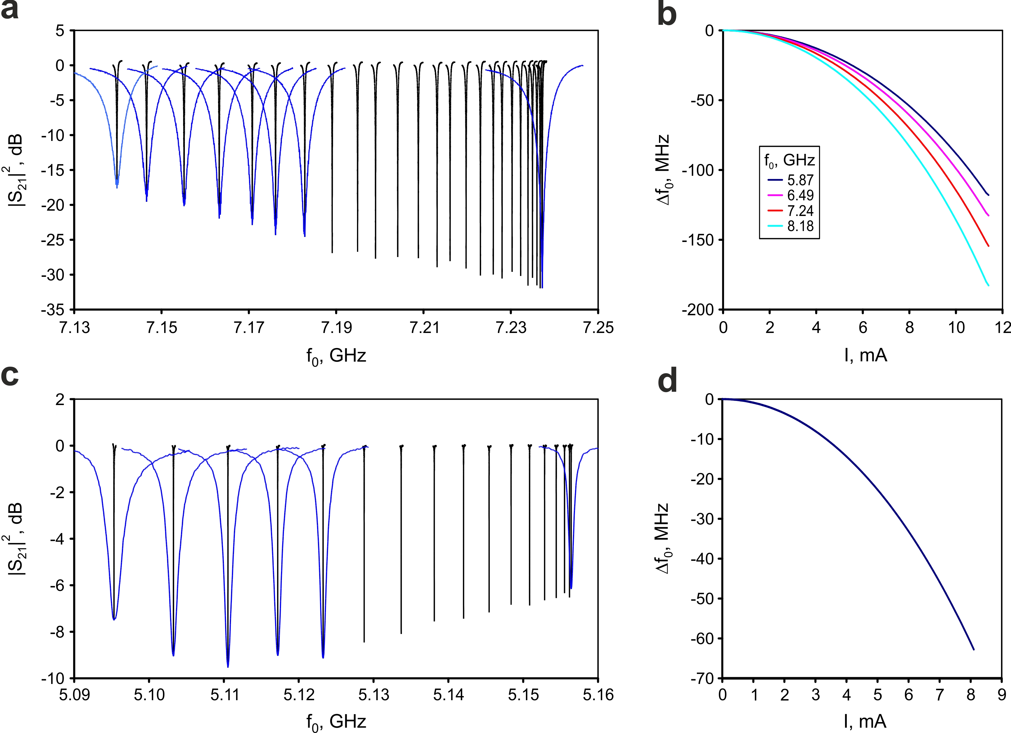
The fabricated devices were initially characterised in a 2 K LHe cryostat. A vector network analyser (VNA) was used to record the forward transmission () of the device; the measured data is shown in Fig. 2 (a,c). The resonance frequency smoothly changes as a function of bias current following a parabolic dependence ( Fig. 2(b,d)) , where is the kinetic inductance at zero current, is the bias current and is the nonlinearity parameter. The extracted from a parabolic fit to Fig. 2(b,d) gives mA such that , where is the critical current of the resonator. These parameters can be to some extent tuned by varying the NbN film deposition conditions such as the substrate temperature, partial pressure and the flow rate.
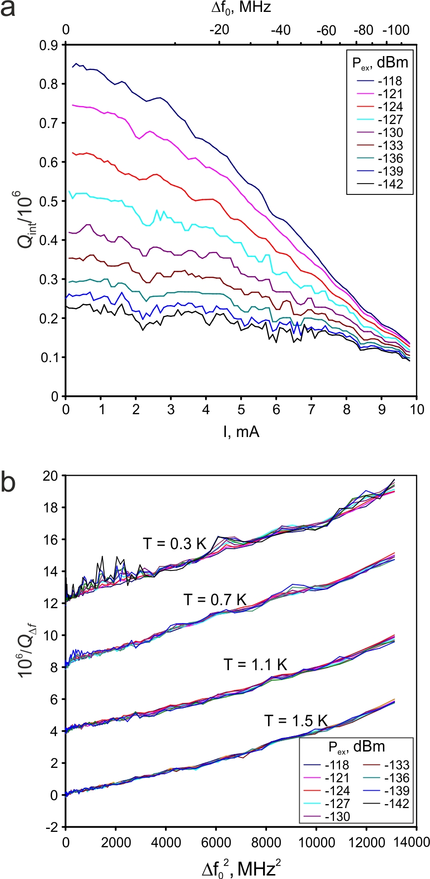
For further characterization, we used a single shot cryostat with a base temperature of 0.3 K. scans were recorded at different temperatures, microwave excitation power levels, and dc tuning currents. From the recorded scans, the internal and coupling quality factors were extracted by fitting the data to the model provided in Probst et al. (2015); the aggregated results are shown in Fig. 3.
Fig. 3(a) presents the internal quality factor as a function of dc tuning for different excitation powers for the measurements taken at 0.3 K. At zero tuning, depends on the excitation power (the power dependence is addressed later). Tuning the resonator frequency induces some excessive dissipation and decreases. Once approaches , the tuning-related part of dissipation starts to dominate and the total -factor does not depend on the excitation power anymore. Similar measurements were also performed at 0.7 K, 1.1 K and 1.5 K. Quantifying the tuning related quality factor as , we compose a plot shown in Fig. 3(b), where is presented as a function of . The fact that does not depend on the excitation power or on the original (non-tuned) clearly indicates that tuning related dissipation is of purely radiative nature. In fact, the quadratic dependence on frequency tuning is what should be expected for radiative losses in our design: the dc current only affects the inductance of the part of the resonator at the closed end (see Fig. 1(a,b)) and does not affect the inductance of the part at the open end. As a result, as the resonance frequency is tuned, the position of the voltage nodes is slightly shifted away from the dc terminal coupling points. The voltage node shift is proportional to , and thus the excessive radiation to . For applications which do not require extreme tuning time as short as , the residual radiation losses can further be suppressed by replacing direct prong-to-ground links with simple low pass filters.
An interesting feature in Fig. 3 are ripples appearing in plots at the near single-photon excitation powers and the lowest temperatures. These ripples are reproducible on short (seconds-to-minutes) timescales and non-reproducible on longer timescales (a couple of hours). We attribute these fluctuations in to interaction with an ensemble of charged two-level systems (TLS), as previously reported in Brehm et al. (2017). At high temperatures/excitation powers, the TLS are saturated and the observed ripples are smeared. Also, as the energies of individual fluctuators are slowly varying in time Müller et al. (2019), the ripple pattern is not reproducible on a longer time scale.
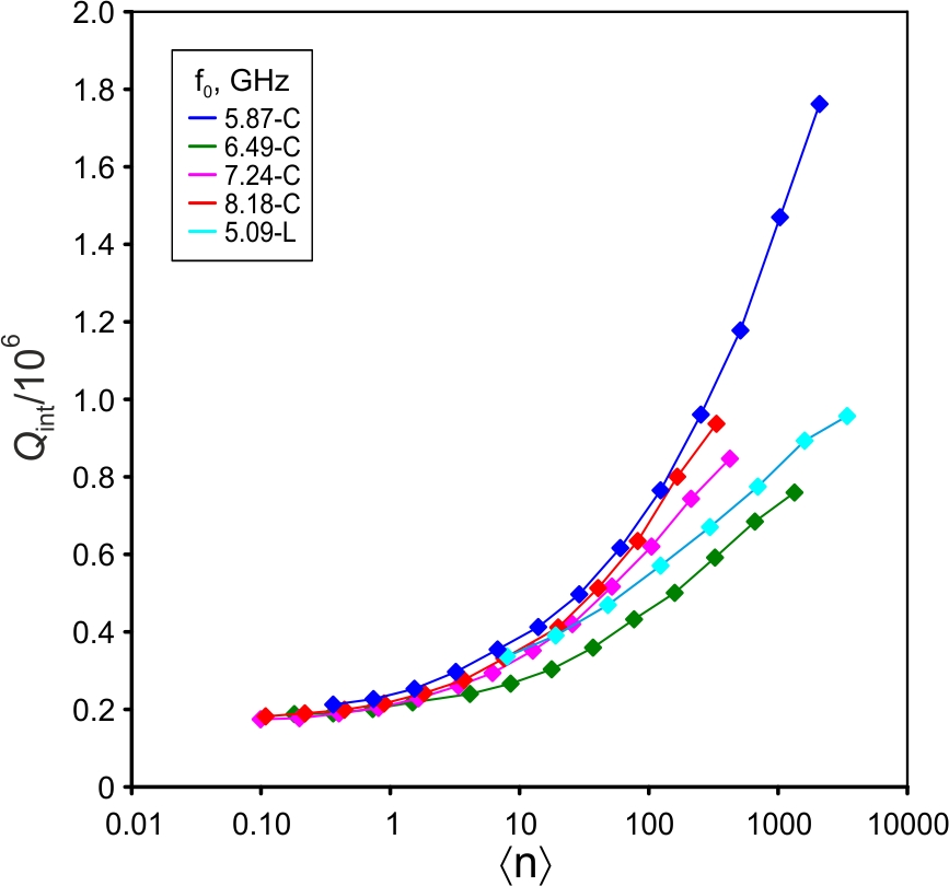
Figure 4 presents the power dependence of for all five resonators at 0.3 K. At near single-photon occupation numbers where TLS losses dominate the total dissipation, is similar for all the devices measured. For high photon occupation numbers, is limited by radiation losses, which varies from device to device by a factor of . We attribute this inconsistency to different residual coupling to parasitics, deviations from left-right symmetry in the prongs of the tuning fork due to fabrication tolerances, etc.
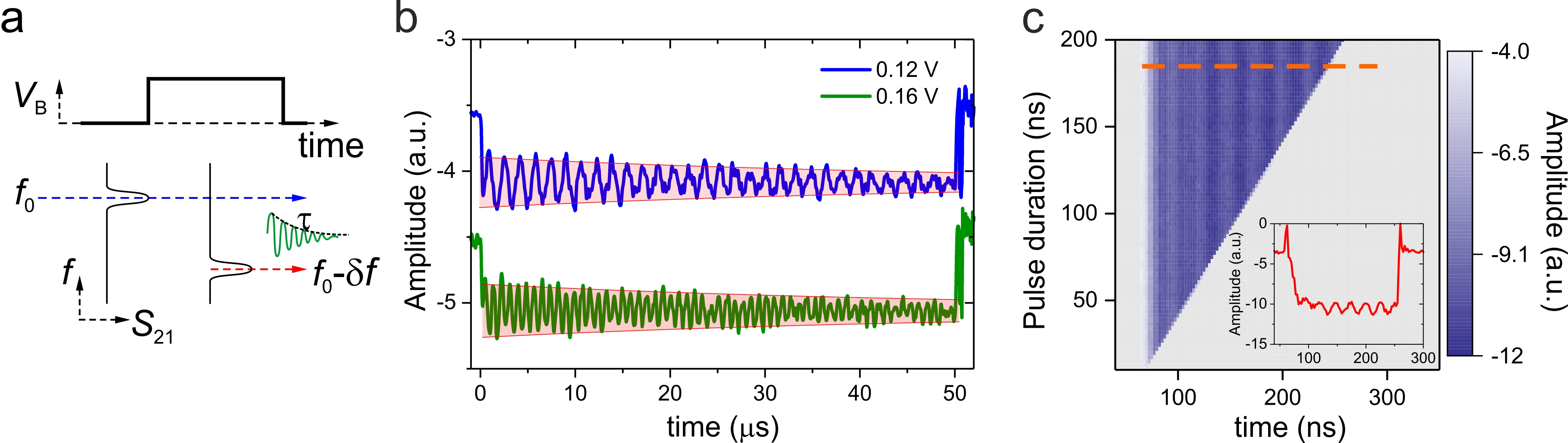
To determine the tuning speed of the resonator we followed the same methodology as in Ref. Sandberg et al. (2008). Figure 5 presents the tuning rate characterization measurements. The resonator is first excited at its unbiased resonance frequency GHz. Then a rectangular current tuning pulse is applied to detune the resonator to . With a homodyne detection scheme, we measure the output microwave power as a function of time, presented in Fig. 5(b). Right after the frequency shift, the output signal is a sum of the excitation power at frequency and the power radiated by the resonator at ; the latter decays on a timescale during which we observe beatings (Fig. 5(b)) in the measured transmitted power. These beatings have a period precisely equal to . By extracting this period we can infer the instantaneous frequency at very short timescales. In Fig. 5(c) we track these beatings down to ns, thus demonstrating an almost instantaneous detuning of 40 MHz, i.e. in a time more than 1000 times shorter than the photon lifetime. We would like to stress that the instantaneous frequency shift of 40 MHz could not be detected in a time shorter than MHz ns, i.e. the reported ns time is actually limited by the resolution of the readout method itself, rather than the internal device response time, that is expected to be even faster.
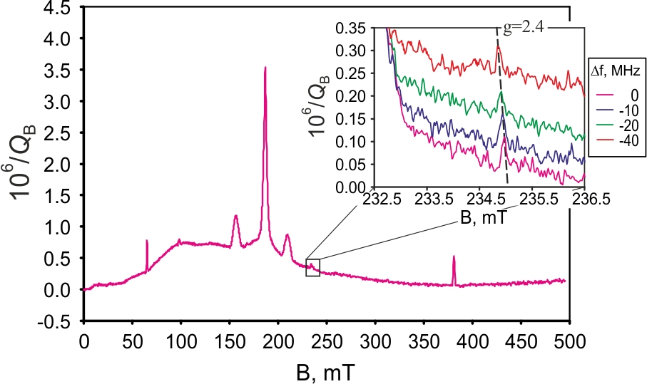
Previously we have demonstrated that the field resilient fractal resonators can be used as a core of on-chip Electron Spin Resonance (ESR) spectrometers de Graaf et al. (2017); De Graaf et al. (2018). Compared to a standard ESR bulk cavity design, the microwave field volume in a planar resonator is squeezed up to times resulting in a greatly enhanced spin-to-microwave coupling. In combination with a high -factor provided by superconducting resonators, this translates to exceptional ESR sensitivity, with a minimum detectable number of spins of a few hundreds Probst et al. (2017); Ranjan et al. (2020). The microwave field in a planar resonator is naturally localized around the substrate surface, which provides selective sensitivity to surface spins and deposited nanoscale clusters de Graaf et al. (2017, 2012). Magnetic field resilience is instrumental for ESR applications, which generally present a challenge for superconducting designs. To achieve high-field resilience we reapply the design ideas previously exploited in de Graaf et al. (2012). Specifically, we implement the fractalized ground plane design to eliminate the magnetic flux focusing. The ground plane in both C- and L-coupled designs is split in such a way that a flux escape path is available for all open (no film) areas, and superconducting loops are thus avoided. Finally (and most importantly), the narrow thin film elements composing a fractal structure effectively expel vortices. Taking all these precautions, we demonstrate that tunable resonators can be made equally suitable for surface spins detection. In Fig. 6, we present an ESR spectrum (i.e. magnetic field dependent dissipation part ) obtained with the tunable resonator by scanning the magnetic field up to 500 mT. From our previous studies we know the number of spins constituting the main ESR peak centered at 180 mT de Graaf et al. (2012). As the area under the peak scales roughly in proportion with the number of constituent spins, the number of spins contributing to a peak positioned at 235 mT (Fig. 6-inset) is estimated to be . Remarkably, even for such a small number of spins the signal-to-noise ratio in Fig. 6-inset is still quite decent. The frequency tuning option provides ESR spectrometer with an additional functionality: by varying the probe frequency by and measuring the corresponding resonance peak shift one can directly assess an equivalent g-factor for the peak in the inset of Fig. 6.
IV Summary
In summary, we have presented a superconducting microwave resonator design which allows for frequency tuning without substantial compromise of the resonator quality factor. We demonstrate that the internal Q-factor holds the value above down to the single photon limit over the entire tuning range up to 200 MHz. The dominant loss mechanism is residual radiation through the current bias control lines which could be further suppressed with low-pass filters. We demonstrated that a full-scale frequency shift can be performed in a time shorter than a fraction of the photon lifetime.
The quasi-fractal resonator design allows for operation in high magnetic fields. Here we demonstrated the magnetic field resilience up to 0.5 T. We argue that by shrinking the minimum design features in the design down to nm or by introducing high-density perforation of the superconducting film the resonators can be made operational in magnetic fields above 5 T, as previously demonstrated in Kroll et al. (2019); Samkharadze et al. (2016).
When the resonator is used for ESR spectrometry, the frequency tuning allows for determination of the effective g-factor of the spins. Owing to a high quality factor of our resonators, the g-factor can be reliably measured on spin ensembles as small as spins, which is close to state of the art in the field Ranjan et al. (2020). In perspective, frequency tunable resonators pave the way for the implementation of advanced ESR techniques with on-chip devices, such as pulsed ESR and ELDOR-NMR Cox et al. (2017). Last, but not least, we foresee many potential applications for fast tunable high- resonators in the rapidly progressing field of quantum computing.
Acknowledgements
The work was jointly supported by the UK department of Business, Energy and Industrial Strategy (BEIS), the EU Horizon 2020 research and innovation programme (grant agreement 766714/HiTIMe), the Swedish Research Council (VR) (grant agreements 2016-04828 and 2019-05480), EU H2020 European Microkelvin Platform (grant agreement 824109), and Chalmers Area of Advance NANO/2018.
References
- Reed et al. (2010) M. D. Reed, B. R. Johnson, A. A. Houck, L. DiCarlo, J. M. Chow, D. I. Schuster, L. Frunzio, and R. J. Schoelkopf, Applied Physics Letters 96, 203110 (2010).
- Wustmann and Shumeiko (2013) W. Wustmann and V. Shumeiko, Physical Review B 87, 184501 (2013).
- Simoen et al. (2015) M. Simoen, C. Chang, P. Krantz, J. Bylander, W. Wustmann, V. Shumeiko, P. Delsing, and C. Wilson, Journal of Applied Physics 118, 154501 (2015).
- Day et al. (2003) P. K. Day, H. G. LeDuc, B. A. Mazin, A. Vayonakis, and J. Zmuidzinas, Nature 425, 817 (2003).
- de Graaf et al. (2013) S. E. de Graaf, A. Danilov, A. Adamyan, and S. Kubatkin, Review of Scientific Instruments 84, 023706 (2013).
- De Graaf et al. (2015) S. De Graaf, A. Danilov, and S. Kubatkin, Scientific reports 5, 17176 (2015).
- Geaney et al. (2019) S. Geaney, D. Cox, T. Hönigl-Decrinis, R. Shaikhaidarov, S. Kubatkin, T. Lindström, A. Danilov, and S. de Graaf, Scientific Reports 9, 12539 (2019).
- Pierre et al. (2014) M. Pierre, I.-M. Svensson, S. Raman Sathyamoorthy, G. Johansson, and P. Delsing, Applied Physics Letters 104, 232604 (2014).
- Yin et al. (2013) Y. Yin, Y. Chen, D. Sank, P. O’Malley, T. White, R. Barends, J. Kelly, E. Lucero, M. Mariantoni, A. Megrant, C. Neill, A. Vainsencher, J. Wenner, A. Korotkov, A. Cleland, and J. Martinis, Physical review letters 110, 107001 (2013).
- Hoi et al. (2011) I.-C. Hoi, C. Wilson, G. Johansson, T. Palomaki, B. Peropadre, and P. Delsing, Physical review letters 107, 073601 (2011).
- Wendin (2017) G. Wendin, Reports on Progress in Physics 80, 106001 (2017).
- Paladino et al. (2014) E. Paladino, Y. Galperin, G. Falci, and B. Altshuler, Reviews of Modern Physics 86, 361 (2014).
- Müller et al. (2019) C. Müller, J. H. Cole, and J. Lisenfeld, Reports on Progress in Physics 82, 124501 (2019).
- de Graaf et al. (2017) S. de Graaf, A. Adamyan, T. Lindström, D. Erts, S. Kubatkin, A. Y. Tzalenchuk, and A. Danilov, Physical review letters 118, 057703 (2017).
- De Graaf et al. (2018) S. De Graaf, L. Faoro, J. Burnett, A. Adamyan, A. Y. Tzalenchuk, S. Kubatkin, T. Lindström, and A. Danilov, Nature communications 9, 1143 (2018).
- Kim et al. (2011) Z. Kim, C. Vlahacos, J. Hoffman, J. Grover, K. Voigt, B. Cooper, C. Ballard, B. Palmer, M. Hafezi, J. Taylor, et al., AIP Advances 1, 042107 (2011).
- Healey et al. (2008) J. Healey, T. Lindström, M. Colclough, C. Muirhead, and A. Y. Tzalenchuk, Applied Physics Letters 93, 043513 (2008).
- Eom et al. (2012) B. H. Eom, P. K. Day, H. G. LeDuc, and J. Zmuidzinas, Nature Physics 8, 623 (2012).
- Chaudhuri et al. (2017) S. Chaudhuri, D. Li, K. Irwin, C. Bockstiegel, J. Hubmayr, J. Ullom, M. Vissers, and J. Gao, Applied Physics Letters 110, 152601 (2017).
- Erickson et al. (2014) R. P. Erickson, M. R. Vissers, M. Sandberg, S. R. Jefferts, and D. P. Pappas, Physical review letters 113, 187002 (2014).
- Sandberg et al. (2008) M. Sandberg, C. Wilson, F. Persson, T. Bauch, G. Johansson, V. Shumeiko, T. Duty, and P. Delsing, Applied Physics Letters 92, 203501 (2008).
- Wang et al. (2013) Z. Wang, Y. Zhong, L. He, H. Wang, J. M. Martinis, A. Cleland, and Q. Xie, Applied Physics Letters 102, 163503 (2013).
- Palacios-Laloy et al. (2008) A. Palacios-Laloy, F. Nguyen, F. Mallet, P. Bertet, D. Vion, and D. Esteve, Journal of Low Temperature Physics 151, 1034 (2008).
- Osborn et al. (2007) K. Osborn, J. Strong, A. J. Sirois, and R. W. Simmonds, IEEE Transactions on Applied Superconductivity 17, 166 (2007).
- Kennedy et al. (2019) O. Kennedy, J. Burnett, J. Fenton, N. Constantino, P. Warburton, J. Morton, and E. Dupont-Ferrier, Physical Review Applied 11, 014006 (2019).
- Svensson et al. (2018) I.-M. Svensson, M. Pierre, M. Simoen, W. Wustmann, P. Krantz, A. Bengtsson, G. Johansson, J. Bylander, V. Shumeiko, and P. Delsing, in Journal of Physics: Conference Series, Vol. 969 (IOP Publishing, 2018) p. 012146.
- Megrant et al. (2012) A. Megrant, C. Neill, R. Barends, B. Chiaro, Y. Chen, L. Feigl, J. Kelly, E. Lucero, M. Mariantoni, P. J. O’Malley, et al., Applied Physics Letters 100, 113510 (2012).
- Bosman et al. (2015) S. J. Bosman, V. Singh, A. Bruno, and G. A. Steele, Applied Physics Letters 107, 192602 (2015).
- Adamyan et al. (2016) A. Adamyan, S. Kubatkin, and A. Danilov, Applied Physics Letters 108, 172601 (2016).
- Vissers et al. (2015) M. R. Vissers, J. Hubmayr, M. Sandberg, S. Chaudhuri, C. Bockstiegel, and J. Gao, Applied Physics Letters 107, 062601 (2015).
- de Graaf et al. (2012) S. de Graaf, A. Danilov, A. Adamyan, T. Bauch, and S. Kubatkin, Journal of Applied Physics 112, 123905 (2012).
- de Graaf et al. (2014) S. E. de Graaf, D. Davidovikj, A. Adamyan, S. Kubatkin, and A. Danilov, Applied Physics Letters 104, 052601 (2014).
- Niepce (2018) D. Niepce, Nanowire Superinductors, Licenciate thesis, Chalmers University of Technology (2018).
- Sonnet Electromagnetic Simulation Software (2019) Sonnet Electromagnetic Simulation Software, http://www.sonnetsoftware.com/products/sonnet-suites/ (2019).
- Probst et al. (2015) S. Probst, F. Song, P. Bushev, A. Ustinov, and M. Weides, Review of Scientific Instruments 86, 024706 (2015).
- Brehm et al. (2017) J. D. Brehm, A. Bilmes, G. Weiss, A. V. Ustinov, and J. Lisenfeld, Applied Physics Letters 111, 112601 (2017).
- Probst et al. (2017) S. Probst, A. Bienfait, P. Campagne-Ibarcq, J. Pla, B. Albanese, J. Da Silva Barbosa, T. Schenkel, D. Vion, D. Esteve, K. Mølmer, et al., Applied Physics Letters 111, 202604 (2017).
- Ranjan et al. (2020) V. Ranjan, S. Probst, B. Albanese, T. Schenkel, D. Vion, D. Esteve, J. Morton, and P. Bertet, arXiv preprint arXiv:2002.03669 (2020).
- Kroll et al. (2019) J. Kroll, F. Borsoi, K. van der Enden, W. Uilhoorn, D. de Jong, M. Quintero-Pérez, D. van Woerkom, A. Bruno, S. Plissard, D. Car, et al., Physical Review Applied 11, 064053 (2019).
- Samkharadze et al. (2016) N. Samkharadze, A. Bruno, P. Scarlino, G. Zheng, D. P. DiVincenzo, L. DiCarlo, and L. Vandersypen, Physical Review Applied 5, 044004 (2016).
- Cox et al. (2017) N. Cox, A. Nalepa, W. Lubitz, and A. Savitsky, Journal of Magnetic Resonance 280, 63 (2017).