[figure]style=plain,subcapbesideposition=bottom \floatsetup[table]capposition=top \shortdate\settimeformatampmtime
Obfuscating the Interconnects: Low-Cost and Resilient Full-Chip Layout Camouflaging
Abstract
Layout camouflaging can protect the intellectual property of modern circuits. Most prior art, however, incurs excessive layout overheads and necessitates customization of active-device manufacturing processes, i.e., the front-end-of-line (FEOL). As a result, camouflaging has typically been applied selectively, which can ultimately undermine its resilience. Here, we propose a low-cost and generic scheme—full-chip camouflaging can be finally realized without reservations. Our scheme is based on obfuscating the interconnects, i.e., the back-end-of-line (BEOL), through design-time handling for real and dummy wires and vias. To that end, we implement custom, BEOL-centric obfuscation cells, and develop a CAD flow using industrial tools. Our scheme can be applied to any design and technology node without FEOL-level modifications. Considering its BEOL-centric nature, we advocate applying our scheme in conjunction with split manufacturing, to furthermore protect against untrusted fabs. We evaluate our scheme for various designs at the physical, DRC-clean layout level. Our scheme incurs a significantly lower cost than most of the prior art. Notably, for fully camouflaged layouts, we observe average power, performance, and area overheads of 24.96%, 19.06%, and 32.55%, respectively. We conduct a thorough security study addressing the threats (attacks) related to untrustworthy FEOL fabs (proximity attacks) and malicious end-users (SAT-based attacks). An empirical key finding is that only large-scale camouflaging schemes like ours are practically secure against powerful SAT-based attacks. Another key finding is that our scheme hinders both placement- and routing-centric proximity attacks; correct connections are reduced by 7.47X, and complexity is increased by 24.15X, respectively, for such attacks.
Index Terms:
Hardware security, IP protection, Reverse engineering, IC camouflaging, Interconnects, Split manufacturing, Boolean satisfiability, Proximity attacks.I Introduction
Ensuring the integrity, security, and trustworthiness of integrated circuits (ICs) have become major concerns in recent years [2, 3]. One important aspect here is that the intellectual property (IP) of modern ICs can be duplicated without consent, resulting in financial losses for IP vendors, which are estimated to amount to several billion dollars per year. This is because modern ICs are the products of distributed and globalized supply chains. If an IC design is not protected, any of the various entities involved in such outsourced supply chains may reconstruct/pirate the underlying IP. Protecting the IP can also help to mitigate other hardware-centric threats, e.g., hardware Trojans [3]. Besides, a malicious end-user, i.e., an adversary without direct access to the design and fabrication process, can resort to reverse engineering of ICs to obtain the IP. The tools and know-how for such reverse-engineering attacks are becoming more advanced and widely available, rendering this a practical and severe threat [3, 4].
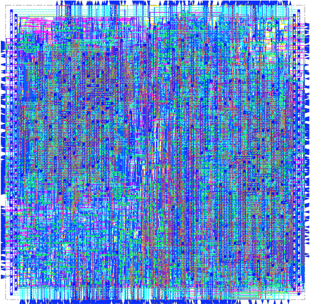
The traditional goal of layout camouflaging (LC), or simply camouflaging, is to mitigate reverse-engineering attacks by end-users. Therefore, camouflaging alters the physical appearance of an IC such that it is arduous for the attacker to understand the true IC design (Fig. 1). In other words, when facing camouflaged ICs, an attacker shall be rendered unable to infer the chip IP directly, as the IP is hidden within an obfuscated physical design.111IP protection can also be realized at the system level, e.g., by obfuscating finite state machines [5]. However, such techniques are orthogonal and independent from the physical obfuscation we consider in this work.
Camouflaging is implemented traditionally at the device layer, e.g., by “look-alike” or ambiguous gates [6, 7], by secretly configured multiplexers [8, 9], or by the threshold-dependent configuration of gates [10, 11, 12]. We note that prior art requires a fully trustworthy fabrication process, as the device obfuscation has to be realized by the foundry. We also note that most schemes incur a high layout cost. For example, the XOR-NAND-NOR primitive proposed in [7] is expected to incur 4 area, 5.5 power, and 1.6 delay cost in comparison to a conventional NAND gate. For another scheme by Akkaya et al. [13], demonstrated in a 65nm chip, an equivalent primitive incurs even higher APD cost, namely 7.3 area (A), 9.2 power (P), and 6.6 delay (D). Accordingly, the application of such schemes is suggested to be limited, which in turn may compromise their resilience as discussed next.
Assuming that prior schemes are applicable only to selected parts of an IC in practice, an essential challenge is where and to what extent camouflaging shall be effected. Ideally, an attacker’s effort to resolve a carefully camouflaged netlist would be exponential in the number of camouflaged gates [14]. To achieve such resilience, among other approaches, Rajendran et al. [7] proposed to camouflage gates that are interfering, i.e., gates that cannot be resolved individually. Still, advances for Boolean satisfiability (SAT) solvers have enabled powerful attacks on camouflaging (and logic locking) [15, 16, 14], undermining the promises of [7] and other works. Even for hardened schemes such as [17, 18, 19], which explicitly aim for exponential attack resilience, tailored SAT and other attack frameworks have been proposed [20, 21, 22, 23]. Therefore, the trade-off between resilience and cost/applicability remains an open challenge for camouflaging.
In Table I, we provide a high-level comparison of the selected prior art and our work. We also discuss the prior art and other relevant security aspects further in Sec. II. Besides, a comprehensive overview of camouflaging is given in [24], and IP protection in general is reviewed in [25, 26].
| Work | LC | Trusted Foundry | LC | APD | Resilience to |
| Style | Assumed? | Scale | Cost | Algorithmic Attacks | |
| [7] | Contact | Yes | “Small” | “Very high” | Vulnerable [14], [This] |
| [17] | Contact/Dopant | Yes | “Small” | “Moderate” | Vulnerable [23] |
| [11] | Dopant | Yes | “Small” | “Very high” | Vulnerable for |
| small-scale LC [This] | |||||
| [27] | Interconnects | Yes | “Small” | “Low” | Vulnerable [This] |
| Ours | Interconnects | Untrusted FEOL, | “Large” | “Moderate” | Superior; attacks |
| trusted BEOL | yet to succeed |
In this paper, we make the following case: to remain resilient, at least as long as foreseeable, camouflaging should be applied at large scales, ideally for the full chip. Alternative approaches are required to enable large-scale camouflaging, especially when aiming for low cost and fewer dependencies on trustworthy fabrication. To that end, we propose and evaluate a novel concept based on obfuscating the interconnects (Fig. 2). Our contributions can be summarized as follows:
-
1.
Based on the emerging notion of obfuscating the interconnects, we enable resilient and large-scale camouflaging, up to full-chip camouflaging. To do so, we develop a security- and cost-driven, end-to-end CAD methodology, and we propose novel back-end-of-line (BEOL)-centric camouflaging primitives which are applicable for all types of regular gates. That is, our primitives do not require any modification at the front-end-of-line (FEOL) layers and can, therefore, be easily integrated into any design, technology, and CAD flow. We leverage Cadence Innovus, and make our layouts publicly available in [28].
- 2.
-
3.
We conduct a thorough evaluation of our scheme concerning the APD (or PPA—power, performance, and area) cost for camouflaged, DRC-clean physical layouts. In contrast, most prior art investigate their camouflaging primitives only as stand-alone devices, without applying them in actual layouts; we argue that this is overly optimistic. Thus, our work is one of the very few providing a comprehensive layout-level evaluation, and we also provide an in-depth and comprehensive study on APD cost for a wide range of prior camouflaging schemes.
-
4.
We assess the resilience of our scheme and compare it against previous works. For our scheme, we introduce the notion of practically secure camouflaging which seeks to impose high computational costs on SAT-based attacks while, unlike provably secure camouflaging, not requiring additional, dedicated circuit structures. For that assessment, we employ powerful SAT-based attacks [31, 32] on traditional benchmarks as well as large VLSI benchmarks. With regards to split manufacturing, we employ state-of-the-art proximity attacks [33, 34] and demonstrate that our scheme is also resilient against such fab-based adversarial activities.
II Background and Motivation
II-A Split Manufacturing
A technique orthogonal to camouflaging is split manufacturing [29, 2, 30]—while camouflaging seeks to protect against malicious end-users, split manufacturing aims to hinder adversaries acting at manufacturing time. Typically, split manufacturing means to split the IC manufacturing flow into FEOL and BEOL processes, i.e., the front-end-of-line and back-end-of-line steps, where the FEOL is outsourced, and the BEOL is realized by some trusted in-house or on-shore facility. Note that split manufacturing has been demonstrated; [30] describes promising measurement results for an IBM/GlobalFoundries 130nm split process, and [29] summarizes further results, most notably for a 28nm split process run by Samsung across Austin and South Korea.
For the FEOL foundry, the resulting partial layout appears as “sea of gates,” with most of the interconnects missing. Therefore, it is argued that an adversary residing in the foundry cannot infer the full design easily, which hinders him/her from both IP piracy and Trojan insertion. The advantages of split manufacturing are as follows: 1) it allows for commissioning high-end, state-of-the-art, yet untrusted, FEOL facilities; 2) the BEOL is significantly less complex and cheap to implement compared to the FEOL and, thus, technology requirements for the trusted facility are moderate; 3) the supply chain can remain largely as is, and additional steps are only required for preparation, shipping, and finalization of FEOL wafers.
Since physical layouts are designed holistically, at least when using regular and security-unaware CAD tools, various hints on the BEOL can remain within the FEOL. Wang et al. [35] proposed a so-called proximity attack, where they formulated various FEOL-level hints within a network-flow attack model.222The hints are: (i) physical proximity of gates, (ii) avoidance of combinatorial loops, which are rare in practice, (iii) timing and load constraints, and (iv) orientation and routing direction of wires. For selected designs, they succeeded to infer the majority of missing BEOL wires. Magaña et al. [36] proposed various attacks that focus on FEOL-level routing, and they conclude that such efforts are more effective than relying solely on the placement. Zhang et al. [37] and Li et al. [38] leveraged machine learning for advanced and scalable attack frameworks. However, neither of those attacks [37, 36, 38] recovers an actual netlist; they instead provide sets of most probable BEOL connections. Therefore, an attacker requires further effort and know-how before he/she can obtain a complete netlist. In any case, attacks which can achieve 100% correctness when inferring all BEOL wires of industrial, large-scale designs, possibly even with some placement- or routing-level perturbations introduced for protection (e.g., see [39, 40, 41, 42]), are yet to be demonstrated.
| Benchmark | Total | Instance Counts of Relevant Cells | Resulting Camouflaging Limit [% of Total Instances] | ||||||||||||||||
| Instances | XOR2 | XNOR2 | OR2 | NOR2 | NAND2 | AND2 | INV | BUF | AND3 | NAND3 | XOR-type | STF-type | XOR-NAND-NOR | Threshold | Ours | ||||
| [17] | [17] | [7] | [11] | ||||||||||||||||
| b14_C | 3,263 | 11 | 143 | 144 | 156 | 930 | 248 | 636 | 23 | 22 | 89 | 68.89 | 58.57 | 33.62 | 50.01 | 100 | |||
| b15_C | 4,972 | 16 | 61 | 133 | 263 | 1,285 | 321 | 844 | 156 | 24 | 128 | 63.44 | 54.4 | 31.46 | 41.81 | 100 | |||
| b17_C | 16,169 | 34 | 207 | 553 | 1,012 | 3,561 | 876 | 3,143 | 536 | 41 | 465 | 63.01 | 54.71 | 28.49 | 38.61 | 100 | |||
| b20_C | 7,184 | 40 | 288 | 318 | 355 | 2,087 | 451 | 1,489 | 117 | 49 | 263 | 71.39 | 61.46 | 34.55 | 49.26 | 100 | |||
| b21_C | 7,318 | 33 | 341 | 407 | 401 | 1,949 | 551 | 1,505 | 110 | 41 | 206 | 70.65 | 60.3 | 32.56 | 50.31 | 100 | |||
| b22_C | 10,839 | 72 | 457 | 544 | 595 | 3,058 | 653 | 2,194 | 170 | 60 | 379 | 70.61 | 61.09 | 34.37 | 49.63 | 100 | |||
| Average | – | – | – | – | – | – | – | – | – | – | – | 67.99 | 58.42 | 32.51 | 46.61 | 100 | |||
We use the NanGate 45nm library [43]. All benchmarks are set up for iso-performance at 5ns. The resulting camouflaging limit (right) is the ratio of cells that can be camouflaged over total cell instances, the latter as obtained by regular synthesis using the full library (left). Cells described as relevant for XOR-type camouflaging in [17]: BUF, INV, AND2, NAND2, OR2, NOR2, AND3, NAND3; cells described as relevant for STF-type camouflaging in [17]: BUF, INV, AND2, NAND2, OR2, AND3; cells assumed relevant for XOR-NAND-NOR camouflaging [7]: XOR2, NAND2, NOR2; cells assumed relevant for threshold-dependent camouflaging [11]: AND2, NAND2, NOR2, OR2, XOR2, XNOR2.
II-B Camouflaging at the FEOL: Limitations and Vulnerabilities
Prior art targets mainly at the active device layer, the FEOL, and, thus, requires (i) custom design of camouflaged gates, along with library characterization, and (ii) some modifications of well-established and optimized device manufacturing processes. It is easy to see that both will incur efforts and financial cost, that is on top of any layout overheads.
Regarding layout overheads, as already indicated in Sec. I, most existing camouflaging schemes incur a high cost and are accordingly limited for practical use. For example for Zhang’s work [9], we observe 464%, 638%, and 63% overheads for area, power, and delay, respectively, when camouflaging all gates of the ISCAS-85 benchmark c7552; these numbers are 13.92, 37.51, and 4.47 higher than ours for the same scenario (see also Sec. VI-B for more comparisons).
Furthermore, it is important to note that prior art can be constrained to begin with, namely by synthesis limiting the extent or scale to which camouflaging is applicable at all. More specifically, most prior arts implement stealthily multiple Boolean functions within customized gate-level structures, but these primitives capture typically only some subsets of all the functionalities needed for modern IC designs. For example, with the XOR2-NAND2-NOR2 primitive proposed in [7], the camouflaging scale is inherently constrained (by synthesis) to the ratio of gates being mapped to XOR2, NAND2, and NOR2.333For FEOL-centric camouflaging, the camouflaging scale would be defined as the ratio of camouflaged gates over the total number of gates in the layout. This definition applies for this particular section, and for the discussion of the prior art throughout this paper. For our BEOL-centric scheme, however, camouflaging scale is defined as the number of obfuscated nets over the total number of nets. It is important to note that these two definitions are compatible; that is because we always obfuscate all the inputs of any gate selected for camouflaging. We explore this limitation for selected schemes in Table II. We note that the limited scales of around 30–40% camouflaging observed for some schemes are not sufficient to protect against SAT-based attacks; see also Sec. VI-C for details. We also note that, as a countermeasure, one may conduct synthesis with constrained libraries that only provide the functions covered by the employed camouflaging primitives. Doing so, however, would incur considerable APD cost over full-library synthesis already for the baseline (Table III), with actual overheads incurred by the camouflaging primitives themselves coming further on top.
| Benchmark | XOR-type [17] | XOR-NAND-NOR [7] | Threshold [11] | |||||||||
|---|---|---|---|---|---|---|---|---|---|---|---|---|
| A | P | D | A | P | D | A | P | D | ||||
| b14_C | 5.63 | -7.25 | -1.85 | 18.24 | 8.81 | -0.27 | 13.24 | 1.21 | -0.27 | |||
| b15_C | 24.99 | 11.79 | -1.06 | 39.05 | 31.93 | -0.79 | 32.35 | 22.79 | -1.99 | |||
| b17_C | 28.38 | 20.13 | 0.99 | 33.96 | 21.81 | -1.25 | 38.18 | 25.09 | 4.92 | |||
| b20_C | 14.14 | -1.38 | 0.64 | 25.62 | 14.97 | -1.07 | 18.39 | 7.76 | 0.04 | |||
| b21_C | 17.25 | 3.11 | 0.27 | 23.11 | 8.86 | 0.76 | 16.19 | -0.06 | 0.37 | |||
| b22_C | 16.29 | 5.24 | -0.79 | 29.88 | 25.32 | 0.49 | 19.25 | 10.71 | 0.21 | |||
| Average | 17.78 | 5.27 | -0.3 | 28.31 | 18.62 | -0.36 | 22.93 | 11.25 | 0.55 | |||
In short, existing schemes can be applied only selectively—if at all—due to their impact on FEOL processing steps, their inherent APD overheads, and their limited scale. As a result, the constrained application of these and other schemes can compromise their resilience, as discussed next.
As mentioned in Sec. I, powerful SAT-based attacks have challenged most prior art on camouflaging (and logic locking) [15, 16, 14]. The idea is that an obfuscated netlist can be modeled as satisfiability problem, where a working chip copy is leveraged as an oracle to iteratively revise the model of the camouflaged netlist, by pruning out step by step any infeasible assignments for the camouflaged gates. The previously unforeseen success of such SAT-based attacks stems from the fact that typically only a small number of I/O patterns are required when resolving various camouflaging schemes.
Several studies on provably secure camouflaging (and logic locking), e.g., see [17, 18, 19, 44], seek to mitigate SAT-based attacks by inserting dedicated structures which necessitate considering an exponential number of I/O patterns. However, the output signals related to such structures have been identified successfully, e.g., by signal-probability- or sensitization-driven algorithms [23, 45, 46]. These critical wires may be ignored or even cut to circumvent the security features. We note that wire cutting has been demonstrated in the past [47], enabling such invasive attacks in principle. Besides, these schemes are also vulnerable to other algorithmic attacks [20, 21, 22, 23]. This is because a key limitation of these schemes is that they induce low output corruptibility, allowing an attacker to obtain relatively easily an approximate version of the IP. Note that this fact also implies that these schemes are less suitable to protect design IP at the chip scale.
Reverse engineering measures may also render FEOL-centric camouflaging directly void, without the assistance of algorithmic techniques. Schemes such as “look-alike” and ambiguous gates [6, 7], or secretly configured MUXes [8, 9] rely on dummy contacts or dummy channels. While yet to be demonstrated, we argue that scanning electron microscopy in the passive voltage mode (SEM PVC) might break these schemes. This is because dummy contacts/channels accumulate charges to a much lower degree than real contacts/channels. Threshold-dependent camouflaging of gates can also be revealed by SEM PVC, as demonstrated successfully by Sugawara et al. [4]. As Collantes et al. [10] indicate themselves, monitoring the etch rates can also reveal different doping levels, which are at the heart of their threshold-dependent gates. Besides, the tailored structures of provably secure schemes may be relatively easy to identify during reverse engineering, as these structures are typically applied only in few places due to their relatively high cost, and they rely on otherwise uncommon, very large combinatorial trees.
Overall, considering these various limitations and vulnerabilities for prior art on FEOL-centric camouflaging, we argue that alternative approaches are necessary. We believe that such novel approaches should foremost be large-scale camouflaging schemes, ideally camouflaging full chips, to 1) remain resilient as long as foreseeable against any algorithmic attacks, and 2) impose the highest efforts for any physical attacks.
II-C Toward Camouflaging at the BEOL
An interesting approach was suggested by Chen et al. [27], namely to obfuscate the interconnects by implementing real, conductive vias using magnesium (Mg) along with dummy, non-conductive vias using magnesium oxide (MgO). Chen et al. elaborated that the use of Mg/MgO is practical from both the perspectives of (i) manufacturability and (ii) mitigation of reverse engineering. For (i), they noted that Mg had been used traditionally to facilitate the bonding of copper interconnects, and both Mg/MgO are compatible with standard processes, in particular sputtering, electron-beam evaporation, and Dual-Damascene. Independently, Swerts et al. [48, 49] and Hwang et al. [50] have used Mg and MgO for customized BEOL processes, albeit without camouflaging in mind. For (ii), Chen et al. fabricated samples and observed that Mg was completely oxidized into MgO within a few minutes. That is, the real Mg vias became indistinguishable from the dummy MgO vias during reverse engineering. Again independently, Hwang et al. [50] have shown that Mg not only oxidizes but also dissolves quickly—as does MgO—when surrounded by fluids. We note that such dissolving would be inevitable for etching and other reverse-engineering procedures.
Although one can argue that reverse engineering of Mg/MgO vias is possible nevertheless, this is yet to be demonstrated. In general, the notion of camouflaging at the BEOL is not limited to materials currently established for manufacturing; future interconnects, e.g., based on carbon/graphene or spintronics [51, 52], may become relevant as well.
It is important to note that obfuscated interconnects, similar to FEOL-centric camouflaging, are implemented not only at the security-enforcing designer’s choice but also at the manufacturer’s discretion. However, obfuscating the interconnects still allows to limit the dependency on outsourced, potentially untrustworthy manufacturing facilities, since only the less complex BEOL part has to remain protected within trusted facilities. We note that split manufacturing is particularly promising in this context (Fig. 3).
Finally, another argument for obfuscating the interconnects is that commercial cost may be compensated for, even when split manufacturing is applied. This is because one requires only additional BEOL processing steps, with BEOL masks being relatively cheap; e.g., for 16nm, M5/M6 masks are 3.5–4 cheaper than Poly masks [53]. In contrast, most FEOL-centric camouflaging (but not necessarily threshold-dependent camouflaging) incurs high cost for the additional FEOL masks. In general, we would like to recall that FEOL-centric camouflaging demands some alterations for devices and their manufacturing process—such alterations are likely more complex and costly than camouflaging at the BEOL.
Despite their pioneering work, Chen et al. did not provide an SAT-resilient scheme; see Sec. VI-C. We also emphasize that our concept and methodology differ significantly from [27]; here, we only leverage their notion of Mg/MgO vias. Moreover, we advocate and enable the obfuscation of interconnects for large-scale, even full-chip camouflaging, by proposing dedicated design-time techniques to handle dummy vias and wires for any gate. In contrast, Chen et al.[27] considered only small-scale, selected use of additional dummy wires/vias.
III Concept and Camouflaging Primitive

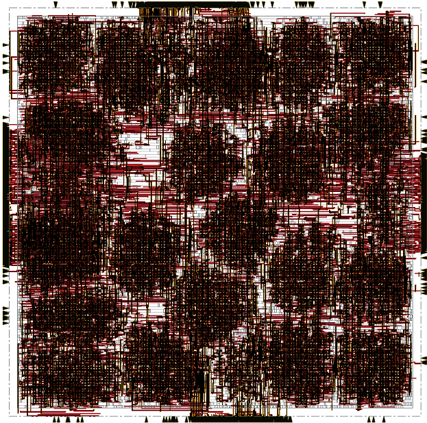
Our key idea is the following: we leverage reverse-engineering-resilient and obfuscated interconnects to design novel, BEOL-centric camouflaging primitives that apply to any regular gate (Fig. 2). We implement wires for each input of the gates to be camouflaged, where of those wires are randomly selected to be acting as dummies, and all wires have their vias obfuscated. In other words, we obfuscate the real inputs of any gate via secret and randomized :1 mapping at the BEOL. As a result, the actual function which a gate implements is obscured in a simple yet effective manner. The set of possible functionalities depends on , the selection of the wires, and on the gate itself; a representative example is given in Fig. 4.
We conducted an exploratory, yet thorough, study on different flavors of our camouflaging primitive. We assessed all flavors when applied at large scales for various benchmarks by 1) their APD cost, while taking our scheme end-to-end and evaluating GDSII layouts, and 2) their resilience against SAT-based attacks while running the seminal attack [15, 31]. The exploratory study is detailed in [1]; we summarize it next.
We first explored the most basic flavor with two wires for each gate’s input, i.e., one randomly selected dummy wire and one real wire. We observed that this flavor offers relatively weak resilience against SAT-based attacks, even for large-scale camouflaging. Therefore, we next extended our primitive for two dummy wires, which provided notably stronger resilience. However, we also noted considerable APD cost for that flavor, due to the following. To hinder an attacker from identifying dummy wires as such, we have to select all the nets for dummy wires randomly but also such that there are no combinatorial loops. Furthermore, dummy wires have to be driven by unique nets, as otherwise some of the possible functionalities could be ruled out directly. These requirements translated to significantly increased routing congestion in practice and, in turn, higher power consumption and delays. Therefore, we note that the use of dummy wires should be limited for large-scale applicability of our scheme. Finally, we explored an extended flavor comprising fixed logic values 0 and 1 along with regular nets (Fig. 4). When compared to employing only regular nets, the benefit of using fixed-value nets is that the latter are not switching, thus exhibiting only negligible power consumption and imposing no timing overhead. Also, many of these wires can have the same driver (but not all, see Sec. V-A), which helped to reduce the routing congestion. Regarding SAT-based attacks, we observed that this flavor provides good resilience.
In short, we select the flavor exemplified in Fig. 4 for the remainder of our study, as we found empirically that it offers the best security-cost trade-off [1].
Since our concept is based on camouflaging at the BEOL, it can be readily applied in conjunction with split manufacturing (Sec. II-A). To that end, we tailor our camouflaging primitive initially for higher metal layers, namely for M5 and M6 (Sec. V-C). We do so because split manufacturing is considered more practical for higher layers [54, 41], as those layers have rather large pitches, which are relatively easy and cheap to manufacture by the BEOL facility. We also explore our camouflaging primitive when tailored for lower metal layers (i.e., M3 and M4 in this work), and we support both types of primitives holistically in our flow (Sec. V-B).
IV Threat Model
We assume both the end-users and the fab to be untrusted. The latter is in direct contrast to the prior art on camouflaging that has to trust the fab because of their FEOL-centric techniques. To hinder fab adversaries, i.e., to protect the secret dummy/true vias and wires in the BEOL layers, we leverage split manufacturing; therefore, we require a trusted BEOL facility.444 In a weaker threat model where the fab is trusted, our scheme and its primitives can still be applied as is, just without need for split manufacturing. The goal of malicious end-users is to reverse engineer the chip’s layout and identify its secret mappings in the BEOL layers—recall that the latter is challenging and yet to be demonstrated (Sec. II-C). Ultimately, both malicious end-users and fab adversaries want to reconstruct the original netlist and its IP. To that end, we assume that end-users employ SAT-based attacks, whereas fab workers launch proximity attacks. We evaluate both threat scenarios in Sec. VI-C and VI-D.
We assume that malicious end-users can get hold of working chips, which are used (i) as oracle for iterative SAT-based attack, and (ii) for reverse engineering of the chip’s layout (as required to model the obfuscated netlist as an SAT problem), but end-users cannot directly infer the secret BEOL mappings. We assume that malicious fab workers have access to the FEOL layers, but not to the BEOL layers. We further assume that both end-users and fab workers have the complete know-how of our scheme, the used design tools, etc. However, the adversaries cannot, by nature, reproduce the randomized selection steps taken throughout our scheme.
V Camouflaging Methodology
V-A Protecting Fixed Values and “Implausible Functionalities”
For large-scale camouflaging using our primitive (Fig. 4), we note that the ubiquitous wires relating to fixed values 0 and 1 may give away clues to an attacker. Such fixed-value wires would be driven by distinct, easy-to-identify TIE cells, and such cells and wires are typically used only selectively, e.g., for special registers or “hardware feature flags.” Therefore, an attacker observing a vast number of fixed-value wires might rightfully assume that these wires have been introduced only for obfuscation, and could try to disregard them. Besides, we have to address another challenge at once: a mindful attacker may also try to rule out all the “implausible functionalities” which are those beyond any gate’s original functionality, i.e., inverter, buffer, and TIE cells, from the search space. Since these functionalities arise only due to the fixed values being part of the obfuscated inputs, they can only become effective once the fixed values are made an essential part of the design, and vice versa.
In short, the fixed-value wires have to be rendered essential parts of the layout, while also protecting all the “implausible functionalities,” of gates. To do so, we perform netlist transformations at the beginning of our methodology as follows:

-
1.
We transform selected inverters (INVs) and buffers (BUFs) into camouflaged gates of other types (e.g., see Fig. 5). Nowadays, around 50% of all gates are repeaters using INV/BUF [55], offering ample opportunities for related transformations. One can freely choose (i) the number of INVs/BUFs to transform and (ii) the type of gate to transform them into following Boolean algebra. For a standard library, for example, INV (BUF) can be implemented using NAND (AND), NOR (OR), as well as both XOR and XNOR, all while using the fixed-value wires as one of the real inputs for those gates. This step renders the fixed-value wires essential—they cannot be ignored anymore without misinterpreting those transformed, camouflaged gates and, therefore, without misinterpreting the whole design. We also note that the “implausible functionalities” INV and BUF are now rendered plausible for the design and, independently, an attacker cannot simply infer a direct relationship between any of the camouflaged gates and their true functionality.
-
2.
We insert additional gates of randomly selected types into randomly selected regions of whitespace. These additional gates are camouflaged as well, with their real inputs tied to fixed-value wires. These gates act as “TIE cells in disguise” and, in turn, they seemingly “drive” other camouflaged gates, which are randomly selected from the vicinity. Therefore, also the “implausible functionalities” 0 and 1 cannot be ruled out anymore without misinterpreting the design. As with the transformation of INV/BUF above, leveraging randomness here is essential to hinder attackers from simply inferring these camouflaged gates.
V-B CAD Flow
Here we provide an overview of our methodology (Fig. 6), which can be easily integrated into any design flow. In this work, we implement our methodology for Cadence Innovus.
Given a netlist, we initially synthesize, place, and route the design. On this original layout, we then apply our netlist transformations outlined above, along with the insertion of TIE cells. Recall that, for our scheme, we define camouflaging scale, or LC scale for short, as the ratio of obfuscated nets over all the nets. Also recall that this is directly comparable to the ratio of camouflaged gates over all the gates, as we always obfuscate all the input nets of any gate selected for camouflaging. Next, depending on the camouflaging scale, we prepare for camouflaging in lower and higher metal layers, e.g., 30% camouflaging in lower layers and 70% camouflaging in higher layers for an camouflaging scale of 100% overall. That so-called metal-layer ratio for lower/higher layers and the camouflaging scale are provided by the user. Then we randomly assign nets to be camouflaged at lower/higher layers, subject to these two parameters.
Next, we insert and connect individual obfuscating cells for all the inputs of each gate to be camouflaged—these cells are essentially implementing our camouflaging primitives. It is essential to understand that these customized obfuscating cells do not impact the FEOL layers—their sole purpose is to enable the routing of all dummy and real wires (Fig. 7). Hence, the physical design of these customized cells is tailored for routability, while their arrangement remains flexible and unconfined concerning the already placed standard cells. See Sec. V-C for more details on the physical design, and see Fig. 8 for a layout snapshot of multiple obfuscating cells in M5/M6.

As already indicated in Sec. III, we have to choose dummy nets carefully such that they are unique concerning each gate to be camouflaged. We do so by applying a local spatial search around each gate’s inputs; nearby nets/wires are preferably selected to limit the routing congestion. We also check for combinatorial loops, which may have resulted during that process and re-select dummy nets as required.
After embedding and connecting the obfuscating cells, we perform trial routing—now with all the dummy wires along with the real wires—and we evaluate the congestion. In case of excessive congestion, the user is tasked to revise (i) the metal-layer ratio and, if need be, (ii) the die outline. Regarding (i), we advocate to revise it toward more utilization of higher layers and less utilization of lower layers for the following reasons. First, we note that lower layers tend to become more utilized in any case, even when obfuscating cells are assigned to higher layers. That is because the related dummy wires can also incur additional wiring throughout the lower layers. Second, we note that obfuscating cells and their vias inserted into the lower layers tend to require even more resources. Regarding (ii), in case congestion remains after exploring various metal-layer ratios, we advocate to enlarge the die outline carefully to gain more routing resources.555An alternative to gain routing resources is to employ additional metal layers, which may also be more economical than enlarging die outlines [41].
Once we obtain an uncongested solution, we perform legalization and ECO optimization; the latter is also based on custom constraint rules, see Sec. V-C. At the same time, we also re-route the design. Drivers are automatically up-scaled as needed to effectively/seemingly drive all the additional true/dummy wiring and the increased fanouts; see also Sec. V-C. We perform final design closure, remove the obfuscating cells from the design, re-extract the RC data, stream out the GDSII data, and gather the final APD/PPA numbers. Note that, after removal of the obfuscating cells, all the true/dummy vias and related wiring remain as such in place of those cells. Thus, the final APD/PPA numbers represent the nature of the camouflaged layout accurately.
V-C Physical Design of Obfuscating Cells
We implement the obfuscating cells as customized cells, which only pertain to the BEOL. To that end, and without loss of generality, we extend the LIB/LEF files of the NanGate 45nm Open Cell Library [43]. Next, we elaborate on the crucial aspects of the cells’ physical design. Besides the design described here for metal layers M5/M6, we also implemented obfuscating cells for M3/M4 in a similar manner.

-
1.
The cells have four input and one output pin (Fig. 7(b)). These pins have been set up in two metal layers: pins A, B, and Y reside in M6, whereas pins C and D are set up in M5. We have chosen two different layers to minimize the routing congestion—in exploratory experiments with all pins in M6, we observed overly high congestion, especially for camouflaging scales beyond 50%.
-
2.
The dimensions of the pins () and their offsets are chosen such that the pins can be placed directly on the respective layer’s tracks (thin yellow grid in Fig. 7(b)); this is to minimize routing congestion further. Also, note the cell’s grey outline beneath the pins; the pins are partially located outside the outline, which is supported. The minimal width is solely to ease its visual differentiation from standard cells at design time.
-
3.
We define custom constraint rules which prevent the pins of different obfuscating cells from overlapping during legalization. These obfuscating cells can, however, freely overlap with any standard cell without inducing routing conflicts. This is because standard cells have their pins exclusively in the lower metal layers. Therefore, we can camouflage the entire design without blocking any valuable standard-cell area.
-
4.
We leverage the timing and power characteristics of BUFX2, i.e., a buffer with a driving strength of 2. Note that a detailed library characterization is not required as obfuscating cells implement BEOL wires and vias only. However, since obfuscating cells are essentially interposed within the paths, a capacitance annotation of subsequent loads is crucial (Fig. 9). Without such annotation, the respective driver might become undersized, as ECO optimization would only consider the wire routed from the driver toward the obfuscating cell and the latter’s BUFX2 input load, but not the camouflaged gate actually to be driven, which is “masked” by the obfuscating cell. It is important to note that this annotation is to be applied for true nets as well as for dummy nets. Otherwise, dummy nets might be identified as such by possibly undersized drivers.
VI Experimental Investigation
VI-A Setup
Setup for physical design: We implement our methodology as custom TCL scripts for Cadence Innovus 16.15. Our procedures incur some runtime costs, as presented in Table IV.
| Benchmark | Original | 20% | 40% | 60% | 80% | 100% |
| LC Scale | LC Scale | LC Scale | LC Scale | LC Scale | ||
| aes_core | 498 | 1,323 | 2,469 | 2,102 | 3,075 | 4,019 |
| b14_C | 178 | 217 | 258 | 313 | 403 | 527 |
| b15_C | 256 | 316 | 376 | 445 | 514 | 639 |
| b17_C | 603 | 901 | 2,497 | 2,640 | 2,930 | 4,378 |
| b22_C | 428 | 573 | 1,105 | 1,771 | 2,221 | 3,652 |
| diffeq1 | 530 | 819 | 1,576 | 2,733 | 4,349 | 6,256 |
| square | 451 | 787 | 1,964 | 2,118 | 4,606 | 5,343 |
| Average | 420.57 | 705.14 | 1,463.57 | 1,731.71 | 2,385.43 | 3,544.86 |
Benchmarks in italics are from the EPFL suite [56], others are from the ITC-99 suite.
We employ the public NanGate 45nm Open Cell Library [43] with ten metal layers. Synthesis is performed using Synopsys Design Compiler (DC) for the slow process corner. The APD analysis is carried out for 0.95V, 125∘C, and the slow process corner, along with a default input switching activity of 0.2—this is a rather pessimistic setup, providing conservative results with “safety margins” and “room for lowering cost.” We obtain power and timing results using Innovus. We configure the initial utilization rates, i.e., for the original layouts, such that the routing congestion remains close to 0%.
Recall that we implement the obfuscation cells as customized cells in two versions, one for higher layers in M5/M6, and one for lower layers in M3/M4. Unless stated otherwise, results are obtained with obfuscating cells embedded exclusively in M5/M6. For experiments with both higher and lower layers being used, we start with only lower layers being utilized, and revise that ratio, without loss of generality and for the sake of simplicity, in steps of 1% toward higher layers.
Setup for security evaluation: We model ours as well as all camouflaging techniques proposed in [7, 8, 9, 11], as outlined in [16]. More specifically, we model ours as individual 4-to-1 MUXes for all the inputs of each gate to be camouflaged, with all the related dummy/true wires connected to the MUXes’ inputs and with two select/key signals. For the netlist transformation steps explained in Sec. V-A, we select 50% of all INVs/BUFs randomly and transform them into various camouflaged gates randomly and the remaining INVs/BUFs are camouflaged as is; both selections are also subject to the overall camouflaging scale.
For a fair evaluation, the same sets of gates are camouflaged across all camouflaging techniques: for a given benchmark, gates are randomly selected once and then memorized.666Any other technique such as maximum clique [7] could be applied here as well. However, El Massad et al. [14] observed that maximum-clique selection, on average, cannot offer a better resilience than random selection. Ten different sets are generated for each benchmark, ranging from 10% to 100% camouflaging scale, in steps of 10%.
For the scenario of malicious end-users, we evaluate our scheme against powerful SAT-based attacks [15, 31, 21, 32] in Sec. VI-C. We note that these attacks were developed for logic locking but are still applicable for our study—logic locking and camouflaging are closely related and can be transformed into one another [16]. We attribute the average runtime of the attacks as an empirical, yet essential, indicator for a design’s resilience; see also the discussion on the notion of practically secure camouflaging in Sec. VI-C.
For the scenario of malicious fab employees, we evaluate our scheme against the powerful open-source proximity attacks [35, 33] and [36, 34] in Sec. VI-D. We conduct experiments for layouts being split after M3 and M4, respectively, which helps us to evaluate the significance of the split layer for our scheme. For [35, 33], we leverage the commonly applied metrics of correct connection rate (CCR), i.e., the ratio of correctly inferred BEOL connections over total BEOL connections, and Hamming distance (HD) and output error rate (OER) [41]; the latter both quantify the functional correctness of the inferred netlist. HD and OER are computed using Synopsys VCS using 100,000 patterns. For [36, 34], since it does not provide any actual netlists, these metrics are not applicable; instead, we leverage the metrics defined in [36], namely virtual pins (vpins), E[LS], and figure of merit (FOM).777The term vpin or virtual pin refers to the top-most, open, or “dangling” end of a FEOL wire, which is a hint for an adversary that a via would be placed there to connect the FEOL with the undisclosed BEOL. By definition, [36, 34] considers only vpins related to two-pin nets. E[LS] is the number of candidate vpins to match with other vpins over a specific region, i.e., the number of possible pairings in the vicinity of some missing BEOL connection. FOM represents the number of possible pairings normalized over the area of the specific region considered. Thus, when applied step wise across the FEOL layout and averaged, FOM serves to quantify the complexity of exploring all possible BEOL connections. Since the attack [36, 34] does not recover any actual netlists, these metrics are essentially indicators for the complexity imposed on subsequent, yet-to-be-proposed attack steps to infer such netlists.
All attacks are executed on a high-performance computing (HPC) facility. Each computational node has two 14-core Intel Broadwell processors (Xeon E5-2680), running at 2.4 GHz. Each node has 128 GB RAM in total, and 4 GB RAM are guaranteed (by the Slurm HPC scheduler) for each attack run. The CPU time-out (labeled as “t-o”) is set to 48 hours.
Benchmarks: We conduct extensive experiments on traditional benchmarks suites (ISCAS-85 and ITC-99) and, for the first time, also on the large-scale EPFL suite [56] (using the original circuits, not the MIG versions). Note that all benchmarks are combinatorial, but our approach can be directly applied to sequential designs as well. We employ custom scripts to convert (i) the original netlists to bench format with two-input gates, as required for the SAT-based attack [31, 15], and (ii) the post-layout netlists to rt and out format, as required for the proximity attack [36, 34]. We release the scripts for (ii) and other related materials in [57].
VI-B Layout Evaluation
We first report in detail on APD cost for our scheme, and we then compare ours to various prior works. Figure 10 illustrates our cost, along with wirelength and load capacitance, for the EPFL benchmark aes_core [56]. Table V reports our cost for this and other selected benchmarks. Note that we consider further benchmarks as well, for various other experiments, throughout this section. Recall that results are in general obtained with obfuscating cells embedded only in M5/M6; in Table VI, we also provide results for obfuscation cells being embedded in M5/M6 and M3/M4 at once.
| Benchmark | Utilization for | 20% LC Scale | 40% LC Scale | 60% LC Scale | 80% LC Scale | 100% LC Scale | ||||||||||||||||
|---|---|---|---|---|---|---|---|---|---|---|---|---|---|---|---|---|---|---|---|---|---|---|
| Original Layout | Area | Power | Delay | Area | Power | Delay | Area | Power | Delay | Area | Power | Delay | Area | Power | Delay | |||||||
| aes_core | 0.4 | 0 | 9.02 | 21.35 | 0 | 13.49 | 27.46 | 14.29 | 15.44 | 29.72 | 25 | 20.22 | 30.94 | 33.33 | 27.76 | 35.72 | ||||||
| b14_C | 0.5 | 0 | 6.43 | 3.64 | 0 | 9.88 | 5.01 | 11.11 | 16.92 | 9.75 | 19.04 | 21.39 | 8.74 | 19.04 | 38.46 | 14.76 | ||||||
| b15_C | 0.5 | 0 | 10.78 | 7.45 | 0 | 11.19 | 10.14 | 11.11 | 14.39 | 11.45 | 25 | 17.27 | 15.74 | 25 | 28.78 | 20.77 | ||||||
| b17_C | 0.5 | 11.11 | 7.16 | 7.19 | 19.04 | 11.13 | 11.22 | 25 | 16.93 | 14.64 | 42.85 | 17.14 | 14.21 | 42.85 | 28.29 | 16.92 | ||||||
| b22_C | 0.5 | 0 | 7.24 | 11.41 | 0 | 13.11 | 14.37 | 11.11 | 15.11 | 14.81 | 19.04 | 25.27 | 15.11 | 25 | 37.48 | 22.41 | ||||||
| diffeq1 | 0.5 | 0 | 5.78 | 3.61 | 0 | 10.64 | 6.54 | 11.11 | 15.87 | 8.49 | 11.11 | 24.19 | 16.79 | 25 | 31.23 | 28.75 | ||||||
| square | 0.5 | 0 | 8.19 | 7.14 | 11.11 | 9.98 | 13.06 | 11.11 | 13.21 | 11.47 | 19.04 | 18.3 | 16.42 | 25 | 25.15 | 22.45 | ||||||
| Average | 0.5 | 1.59 | 7.8 | 8.83 | 4.31 | 11.35 | 12.54 | 13.55 | 15.41 | 14.33 | 23.01 | 20.54 | 16.85 | 27.89 | 31.02 | 23.11 | ||||||
Layout cost are in percentage. Obfuscating cells are embedded exclusively in M5/M6. Benchmarks in italics are from the EPFL suite [56], others are from the ITC-99 suite. All layouts are DRC-clean and devoid of congestion.
On die area: Recall that our obfuscating cells impact only the metal layers; they do not increase the standard-cell area. Since wiring cannot be expressed by standard-cell area, the reported area cost is concerning die outlines as explained next.
Especially for large-scale camouflaging, with the additional wiring imposed by our scheme requiring significant routing resources, we can observe routing congestion and DRC issues. Recall that we first revise the metal-layer ratio, e.g., see Fig. 11, and, if need be, scale-up die outlines. In other words, we ultimately maintain that our large-scale camouflaged layouts are “DRC-clean” at the cost of larger outlines. For simplicity, we scale-up the outlines by decreasing the utilization rate in steps of 0.05 and 0.02, as appropriate. For example, while relaxing the utilization from 0.5 to 0.45, the die area has to be increased by 11.11%.
| LC Scale | b14_C H | b14_C L&H | b15_C H | b15_C L&H | ||||||||||
|---|---|---|---|---|---|---|---|---|---|---|---|---|---|---|
| P | D | P | D | L/H | P | D | P | D | L/H | |||||
| 20% | 6.43 | 3.64 | 0.87 | -1.08 | 15/5 | 10.78 | 7.45 | 2.94 | 1.46 | 15/5 | ||||
| 40% | 9.88 | 5.01 | 2.17 | 1.99 | 10/30 | 11.19 | 10.14 | 9.43 | 5.94 | 15/25 | ||||
| 60% | 16.92 | 9.75 | 16.12 | 7.18 | 20/40 | 14.39 | 11.45 | 11.75 | 9.98 | 20/40 | ||||
| 80% | 21.39 | 8.74 | 14.27 | 8.24 | 30/50 | 17.27 | 15.74 | 13.68 | 12.22 | 20/60 | ||||
| 100% | 38.46 | 14.76 | 19.91 | 18.76 | 30/70 | 28.78 | 20.77 | 16.99 | 17.29 | 20/80 | ||||
| Average | 18.62 | 8.38 | 10.67 | 7.02 | – | 16.48 | 13.11 | 10.96 | 9.38 | – | ||||
Layout cost and metal-layer ratios (L/H) are in percentage, with the latter being subject to the camouflaging scale (LC). For a fair comparison, the same die outlines are considered for both the H and L&H setups. Note that the cost for the H setup are the same as in Table V.
The average area overheads in Table V are not more than 14% for up to 60% camouflaging scale, whereas for full-chip camouflaging, we note an average area cost close to 28%. Again, these overheads enable DRC-clean layouts even for full-chip camouflaging; we believe that this is a justifiable cost.
Finally, while the transformation of 50% of INV/BUF gates and the insertion of “TIE cells in disguise“ both still incur some standard-cell area cost, this cost is negligible compared to the die cost related to all the additional wiring. In fact, we have conducted additional experiments for full-chip camouflaging of the large-scale EPFL benchmark aes_core [56] for ranges of 25–100% of INVs/BUFs selected for transformation; we did not observe any additional die costs there.
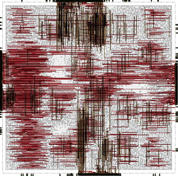
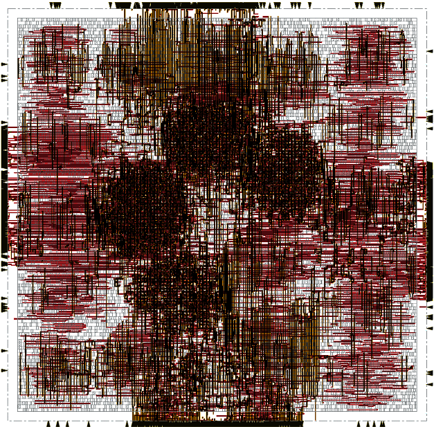
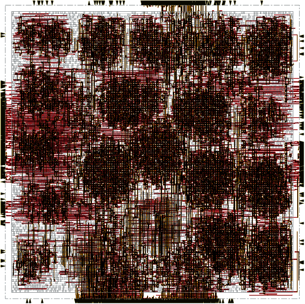
On power and performance: As our camouflaging primitive incurs additional wiring, which becomes significant for large-scale camouflaging, an impact on power and performance is expected. See also Fig. 12 for wiring snapshots across camouflaging ranges.
For camouflaging up until 60% of the layout, the average power and delay overheads are moderate for most benchmarks, around 6–17% for power and 4–15% for delay (Table V). Only for EPFL benchmark aes_core, delays are consistently larger, by approximately 15%. The overheads increase naturally toward full-chip camouflaging, but still follow linear growth trends. We believe that this is due to the following:
-
1.
Besides the transformed INV/BUF gates, all gates remain as is. Even for these transformed gates, cost are limited: for experiments on varying ranges of INVs/BUFs transformed for full-chip camouflaging of the large-scale EPFL benchmark aes_core [56], we observed variations for power and performance cost of less than 9%. That is, we experience no inherent overheads for the majority of gates and marginal overheads for transformed gates.
-
2.
The lower resistance of higher metal layers, which are typically leveraged by most of the obfuscating-cell instances, helps to limit the delay cost.
-
3.
The nets for fixed-values 0 and 1 are not switching and, thus, they neither increase power nor delay. Also, while dummy nets are switching, they drive only wiring loads.
-
4.
For large-scale camouflaging, the positive effects are eventually offset by a steady increase of dummy nets and wiring for camouflaged gates, thereby raising the capacitive loads and power consumption as well as routing congestion. Since congestion can only be managed by re-routing in some detours, this lengthens parts of the wires further. In turn, this also impacts power and delay.
Regarding the use of obfuscating cells in both lower and higher metal layers (Table VI), we observe the following. First, utilizing lower and higher layers at once (L&H setup) allows to reduce cost, especially for power—in contrast to utilizing only the higher layers (H setup), we observe a reduction of 7.95% and 5.52% in power for the ITC-99 benchmarks b14_C and b15_C, respectively, and the delay reduction is 1.36% and 3.73% for the same benchmarks. To explain these trends, we also determine the load capacitance overheads for both setups: for the H setup, the capacitance overhead is about 62.78%, whereas this overhead is reduced to 29.99% for the L&H setup. Second, for large-scale camouflaging, the usability of lower layers becomes less; recall the related discussion in Sec. V-B. Finally, recall that splitting at higher layers is considered beneficial [54, 41], but here we cannot split above the lowest layer containing some camouflaging primitives. Therefore, while the holistic use of lower and higher layers can help to reduce layout cost, it limits the practicality of split manufacturing. For a weaker threat model with the fab being trusted, however, this approach would become more relevant.
Comparison at RTL level and for small-scale camouflaging: Previous works typically report their cost only for small-scale camouflaging and based on RTL simulations, which seems impractical. For example, Rajendran et al. [7] observe 60%, 40%, and 30% increase in area, power, and delay, respectively, when camouflaging 5% of gates in the ISCAS-85 benchmark c7552. The approach of Wang et al. [8] exhibits 50% delay and 15% area overhead already for 5% camouflaging scale. For another, more relevant example, Chen et al. [27] report 3.68% delay and 3.93% area overhead on average, i.e., when configuring their scheme for 3% power budget/overhead and while obfuscating only tens to few hundreds of wires for the ITC-99 benchmarks.
Comparison on physical-layout level: Recall that our work is one of the very few to evaluate camouflaging on placed-and-routed GDSII layouts. When contrasting to a previous study, conducted by Malik et al. [58], we notice significantly higher overheads for them. We note that Malik et al. implement and evaluate their approach exclusively for one AES S-box, which has a far lower number of gates, namely 421, when compared to all the benchmarks we consider. However, we argue that a qualitative comparison is still fair as Malik et al. use the same NanGate library [43]. They reported overheads of 7.09, 6.45, and 3.12 for area, power, and delay (APD), respectively, for their case study. Moreover, Malik et al. indicate themselves that cost will increase for larger circuits.
Besides a provably secure scheme, Li et al. [17] propose two “regular” camouflaging primitives (based on obfuscated contacts), called STF-type and XOR-type. As Li et al. report only gate-level cost for their primitives, we conduct a layout-level comparison for full-chip camouflaging ourselves (Table VII). Here we first constrain synthesis accordingly (recall Sec. II-B), and then we map their gate-level cost to all the gates—this extrapolation is conservative as it implies only a linear scaling even for full-chip camouflaging. While the STF-type primitive becomes a contender to ours in terms of power and delays, it still incurs 23.88% larger die-area cost on average.
For Zhang’s work [9], as its MUX-based primitive is not made available, we implement it ourselves, by using MUXes and INVs for the primitives, and primary inputs for their key bits, and we perform a detailed layout-level evaluation. For example, we observe 464%, 638%, and 63% increase for APD, respectively, when camouflaging all the gates for the ISCAS-85 benchmark c7552. These numbers are 13.92, 37.51, and 4.47 higher than ours for the same scenario.
On average, across all ISCAS-85, ITC-99, and EPFL benchmarks, our scheme incurs only 32.55%, 24.96%, and 19.06% APD cost for full-chip camouflaging.
| Bench- | XOR-type [17] | STF-type [17] | Threshold [12] | Ours | |||||||||||
|---|---|---|---|---|---|---|---|---|---|---|---|---|---|---|---|
| mark | A | P | D | A | P | D | A | P | D | A | P | D | |||
| c432 | 66.48 | 11.43 | 42.2 | 54.31 | 20.37 | 6.4 | 140 | 8 | 96 | 27.27 | 25.46 | 15.41 | |||
| c5315 | 92.33 | 33.81 | 50.56 | 62.18 | 38.31 | 7.29 | 200 | 10 | 76 | 50 | 10.19 | 9.94 | |||
| c7552 | 80.86 | 58.94 | 29.64 | 62.53 | 63.42 | 14.86 | 175 | 9 | 90 | 33.33 | 17.01 | 14.09 | |||
| b14_C | 40.43 | -5.41 | 41.6 | 42.23 | 13.11 | 22.9 | N/A | N/A | N/A | 19.04 | 38.46 | 14.76 | |||
| b15_C | 67.07 | 16.36 | 37.13 | 65.4 | 30.77 | 19.54 | N/A | N/A | N/A | 25 | 28.78 | 20.77 | |||
| b17_C | 71.40 | 25.12 | 55.97 | 59.91 | 11.99 | 14.39 | N/A | N/A | N/A | 42.85 | 28.29 | 16.92 | |||
| b22_C | 46.37 | 7.67 | 47.65 | 43.09 | 25.17 | 25.87 | N/A | N/A | N/A | 25 | 37.48 | 22.41 | |||
| Average | 66.42 | 21.13 | 43.54 | 55.66 | 29.02 | 15.89 | 171.67 | 9 | 87.33 | 31.78 | 26.52 | 16.33 | |||
We consider selected ISCAS-85 and ITC-99 benchmarks, as done in the listed prior art. All layout cost are in percentage. We evaluate cost for [17] ourselves, while constraining synthesis and applying a linear scaling of baseline camouflaging primitives cost, reported in [17], capturing all gates. Cost for [12] are quoted. N/A means not available, i.e., the respective authors did not consider that benchmark.
Comparison with threshold-dependent camouflaging: Nirmala et al. [11] proposed a promising concept of threshold-dependent camouflaging switches. Since their primitive and related libraries are not made available, we apply our own layout-level evaluation as follows. First, we conduct a constrained synthesis run (recall Sec. II-B) using the NanGate library [43]. Then, based on the overhead numbers reported for their primitive, we scale up the cost accordingly for all the camouflaged gate instances. Again, while this is an extrapolating approach, we argue that it is fair, as we reflect truthfully the different overheads for different types of gates camouflaged. We find that the approach by Nirmala et al. will incur significant APD cost for full-chip camouflaging: 1,360%, 1,266%, and 100%, respectively. For the work of Collantes et al. [10], we observe a linear trend in the reported layout cost; simply extrapolating those numbers for full-chip camouflaging would translate to 78% and 147% for power and delay, respectively. Finally, for the work of Erbagci et al. [12], we quote their numbers in Table VII.
Comparison with provably secure camouflaging: Recall that schemes like [19, 18, 17] rely on additional circuitry to protect individual, selected gates, wires, or outputs. Such circuitry can incur a high cost, especially for area and power. Using the benchmarks provided by Amir et al. [59] on trust-hub.org, we conduct a layout-level analysis for Anti-SAT [19], namely for Anti-SAT with random logic locking (RLL) and for Anti-SAT with secure logic locking (SLL) [60].888Recall that locking and camouflaging are interchangeable, especially w.r.t. SAT-based attacks [16], rendering this analysis relevant for our work. We perform a regular design flow here, using the Nangate 45nm library [43] at the slow corner and with timing constrained to 4ns. When comparing these schemes to our full-chip camouflaging (Table VIII), we observe that average overheads are notably larger, namely by 8.95 and 9.59 for area and by 23.66 and 26.05 for power, respectively; only delay overheads are less. We note that these cost arise for protecting single outputs and increase further if we would protect more outputs.
In any case, we emphasize again that our notion of full-chip camouflaging is different from such schemes (including functional obfuscation [22] discussed next), see also on the notion of practically secure camouflaging further below.
| Benchmark | Anti-SAT+RLL | Anti-SAT+SLL | Ours | |||||||||
|---|---|---|---|---|---|---|---|---|---|---|---|---|
| A | P | D | A | P | D | A | P | D | ||||
| c880 | 588.48 | 678.13 | 5.29 | 568.42 | 618.15 | 7.89 | 27.27 | 23.28 | 19.63 | |||
| c1355 | 480.15 | 410.09 | 16.45 | 500.44 | 418.83 | 16.13 | 40 | 9.48 | 11.62 | |||
| c1908 | 479.06 | 526.91 | 2.74 | 552.91 | 644.49 | 3.82 | 40 | 21.11 | 16.46 | |||
| c3540 | 193.87 | 162.05 | 0.92 | 290.07 | 335.75 | 0.31 | 50 | 10.34 | 10.24 | |||
| c5315 | 230.15 | 212.91 | 2.08 | 224.59 | 193.83 | 0.65 | 50 | 10.19 | 9.94 | |||
| c7552 | 182.22 | 173.21 | -4.42 | 170.92 | 170.64 | -4.83 | 33.33 | 17.01 | 14.09 | |||
| Average | 358.99 | 360.55 | 3.84 | 384.56 | 396.95 | 3.99 | 40.1 | 15.24 | 13.66 | |||
All layout cost are in percentage. We use trust-hub.org benchmarks [59] as follows. For Anti-SAT+RLL, we use c880-NR4360, c1355-NR3790, c1908-NR3550, c3540-NR4060, c5315-NR7900, and c7552-NR8770. For Anti-SAT+SLL, we use c880-NS4360, c1355-NS3790, c1908-NS3550, c3540-NS4060, c5315-NS7900, and c7552-NS8770. All protected designs are configured for iso-performance at 4ns.
Comparison with functional obfuscation: Xu et al. [22] proposed binary decision diagram (BDD)-based obfuscation which operates at the functional level, in contrast to other approaches working at the netlist level. It was shown that their scheme can be tailored to remain resilient against SAT-based attacks as well “removal attacks” [22, 23]. As above, we evaluate two approaches of [22] at layout level, namely random obfuscation and Anti-SAT-inspired obfuscation [59]. Again, expect for delay, we observe that average overheads are significantly larger, namely by 92.39 and 76.57 for area and 197.1 and 246.7 for power, respectively (Table IX).
| Benchmark | Random Obfus. | Anti-SAT Obfus. | Ours | |||||||||
|---|---|---|---|---|---|---|---|---|---|---|---|---|
| A | P | D | A | P | D | A | P | D | ||||
| c880 | 5,166.86 | 6,351.69 | 8.14 | 5,289.19 | 6,536.58 | 9.44 | 27.27 | 23.28 | 19.63 | |||
| c1908 | 5,727.6 | 5,973.24 | 1.96 | 7,078.33 | 7,349.63 | 2.74 | 40 | 21.11 | 16.46 | |||
| c3540 | 2,803.79 | 2,111.32 | 1.76 | 2,807.78 | 2,119.05 | 2.32 | 50 | 10.34 | 10.24 | |||
| c5315 | 76.89 | 45.49 | 7.26 | 51.63 | 39.59 | 6.67 | 50 | 10.19 | 9.94 | |||
| c7552 | 109.30 | 63.49 | 0.81 | 133.57 | 97.04 | -0.33 | 33.33 | 17.01 | 14.09 | |||
| Average | 3,706.84 | 4,040.95 | 4.72 | 3,072.1 | 3,228.38 | 4.17 | 40.12 | 16.38 | 14.07 | |||
All layout cost are in percentage. We use trust-hub.org benchmarks [59] as follows. For Random Obfus. we use c880-BR320, c1908-BR320, c3540-BR320, c5315-BR320, and c7552-BR320. For Anti-SAT Obfus. we use c880-BS320, c1908-BS320, c3540-BS320, c5315-BS320, and c7552-BS320. Note that trust-hub.org [59] does not provide the related c1355 circuits. All protected designs are configured for iso-performance at 4ns.
VI-C Security Evaluation: Malicious End-Users, SAT-Based Attacks
On the notion of practically secure camouflaging: Recall that the primary objective for this work is large-scale camouflaging, and an important observation is that this achieves practically secure camouflaging. That is, by camouflaging up to 100% of the layout, we can induce significant computational efforts for SAT-based attacks, without leveraging additional provably secure structures.
Still, it is not straightforward to prove beforehand to what extent large-scale camouflaging will render a layout resilient without actually leveraging a SAT solver’s capabilities for de-camouflaging attacks. Li et al. [17] have shown that de-camouflaging efforts scale on average with (i) the solution space concerning all possible functionalities of the whole design and (ii) the Hamming distances among those different functionalities. A further theoretical evaluation of large-scale camouflaging is difficult since depends on (i) the number and composition of possible functionalities supported by the camouflaging primitives, (ii) the number of camouflaged gates, (iii) the selection of camouflaged gates, and (iv) the interconnectivity of the design, all at the same time. For example, designs containing XOR/XNOR and/or multipliers are harder to de-camouflage in practice than other designs [16, 15].
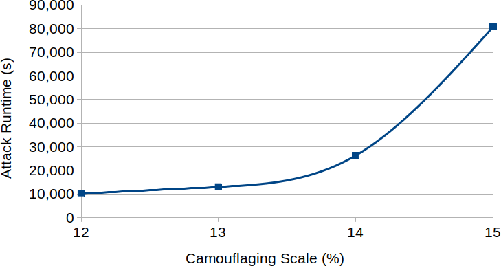
In short, while one can easily estimate the upper bound of , this may not reflect on the actual efforts required for successful attacks. Hence, we next resort to an empirical but comprehensive study. As we observe in this study, we can indeed expect prohibitive runtimes for large-scale camouflaging. More specifically, e.g., we observe a polynomial trend for attacking the benchmark aes_core, setting in around 14% camouflaging (Fig. 13). Similar observations have also been made by Yu et al. [16], albeit for a different primitive and the much smaller benchmark c432 with 209 two-input gates; even such a small layout could not be resolved within three days.
Comparison with prior art on large-scale camouflaging: In Table X, we list runtimes for the seminal SAT-based attack [15, 31], evaluating our camouflaging primitive and those of [7, 8, 9, 11]. Note that these prior studies did not report on any SAT-based attacks for large-scale camouflaging themselves. Also, recall that we camouflage the same sets of gates across all techniques for a fair comparison for each run, and that we report average runtimes over ten such runs.
For our scheme, we do not observe any significant differences for the average SAT-based attack runtimes when considering different ranges of INVs/BUFs being transformed (Sec. V-A). This is because, for cases with less INVs/BUFs being selected for transformation, more other gates are selected for camouflaging, while the overall count of camouflaged gates remains the same; recall that we use the camouflaging scale as design-wide “knob” for all of our experiments.
We note that none of the layouts can be de-camouflaged within 48 hours once full-chip camouflaging is applied. In fact, almost all layouts remain already resilient beyond 40% camouflaging scale; the only exception arises for the ISCAS-85 benchmark c7552 when the most simple camouflaging primitive [9] is leveraged. We ran further exploratory attacks for 7 days on large-scale camouflaging using our primitive—without observing any improvement for the attack. For a more meaningful comparison, we also consider relatively small camouflaging scales, i.e., 10% up to 30%. Here, the primitive by Zhang et al. [9] appears as the weakest and that by Wang et al. [8] as the most resilient. Our primitive is next only to those of [8, 11]. However, it is also important to recall that ours incurs significantly less APD cost (Sec. VI-B).
We also leverage the Double DIP attack, provided by Shen et al. [21, 32]. The crux of their attack is that it can rule out at least two incorrect keys during the application of one single distinguishing input pattern (DIP) for the oracle. While conducting the same set of experiments as above, we observe that the average runtimes are even higher across all benchmarks and camouflaging schemes (Table XI). For example, for the ITC-99 benchmark b14_C with 10% camouflaging applied using our primitive, we observe 137 seconds for [31], but 402 seconds for [32]. Thus, we conclude that Double DIP, while successful for attacking dedicated protection schemes such as SARLock cannot cope well with large-scale camouflaging schemes in general.
Overall, we are not claiming that large-scale camouflaging, whether based on prior art or our primitive, cannot be resolved eventually using SAT-based attacks. Rather, we provide strong empirical evidence that practically secure camouflaging, i.e., once 50–100% of all gates are camouflaged, imposes prohibitive computational cost on SAT solvers.
On the (lack of) resilience for [27]: Since our work is inspired to some degree by that of Chen et al. [27], it seems imperative to investigate the resilience of their scheme as well, especially since Chen et al. did not consider any SAT-based attacks themselves. In Table XII, we note that the SAT-based attack [15, 31] can distinguish between real and dummy interconnects within relatively short runtimes, no matter how many interconnects are obfuscated, i.e., at least concerning the delay constraints defined in [27]. That is, an overly constrained obfuscation as proposed in [27] cannot withstand powerful SAT-based attacks. Similar observations have been also reported by Yu et al. [16].
VI-D Security Evaluation: Fab Adversaries, Proximity Attacks
Similar to the observations made for SAT-based attacks, here we find that our scheme of obfuscating the interconnects—along with all the additional wiring going through both the FEOL and BEOL—serves also well to hinder proximity attacks. That is essentially due to vast numbers of wires being cut at the split layer, creating a large solution space for the attacks to work on. Besides, recall that the metrics used in this section have been introduced in Sec VI-A.
We execute the seminal network-flow attack [35, 33] on different layouts for major camouflaging scales and for two split layers, M3 and M4, on selected ISCAS-85 benchmarks (Table XIII).999We execute the attack also for the larger ITC-99 benchmarks, but it failed to conclude within 48 hours. As indicated, we observe that our scheme is effective in mitigating this attack. The average CCR observed for original layouts is significantly reduced for fully camouflaged layouts, namely by 7.48 and 2.41 when split after M3 and M4, respectively. This significant reduction in CCR is corroborated by the increase of cut wires to handle when attacking our scheme, reported as cut inputs (CI) [33] in Table XIII. For example for the ISCAS-85 benchmarks c5315 and c7552, CI is increased by 4.61 and 7.98, respectively, when comparing fully camouflaged to regular layouts, both split after M3. Again, this increase in CI is due to the fact our scheme routes all nets related to the camouflaging primitive through higher layers.
| Benchmark | 10% Camouflaging Scale | 20% Camouflaging Scale | |||||||||||
| [9] | [7] | [7] | [11] | [8] | Our | [9] | [7] | [7] | [11] | [8] | Our | ||
| (2)∗ | (3)∗ | (4)∗ | (8)∗ | (16)∗ | (10–14)∗ | (2)∗ | (3)∗ | (4)∗ | (8)∗ | (16)∗ | (10–14)∗ | ||
| b14_C | 13.77 | 36.12 | 87.14 | 230.05 | 9,735.42 | 136.66 | 31.09 | 186.46 | 794.64 | 39,341.2 | 48,399.9 | 6,674.53 | |
| b15_C | 20.93 | 77.24 | 172.27 | 1,010.27 | 5,070.97 | 708.31 | 69.21 | 621.75 | 1,592.64 | 8,938.47 | t-o | 4,375.3 | |
| b17_C | 256.71 | 1,174.39 | 2,103.08 | 23,408.4 | t-o | 15,807.3 | 864.55 | 11,202.6 | 30,629 | t-o | t-o | t-o | |
| b20_C | 56.35 | 176.81 | 323.81 | 1,909.9 | 8,755.17 | 1,117.02 | 160.731 | 1,839.28 | 22,371.4 | 56,492.6 | t-o | t-o | |
| b22_C | 121.25 | 446.33 | 1,128.02 | 6,289.34 | 25,814.6 | 2,864.64 | 1,291.26 | 10,835.2 | 22,309.8 | t-o | t-o | t-o | |
| c3540 | 1.47 | 3.32 | 4.08 | 12.04 | 27.72 | 22.02 | 3.58 | 7.88 | 16.10 | 54.24 | 599.95 | 50.80 | |
| c5315 | 0.65 | 1.85 | 4.03 | 12.88 | 22.90 | 7.73 | 1.86 | 7.11 | 20.90 | 144.18 | 369.28 | 44.57 | |
| c7552 | 1.13 | 21.39 | 8.62 | 33.54 | 132.96 | 19.89 | 4.53 | 35.26 | 106.64 | 237.83 | 884.75 | 219.79 | |
| 30% Camouflaging Scale | 40% Camouflaging Scale and Beyond§ | ||||||||||||
| b14_C | 115.78 | 1,659.75 | 14,180.7 | t-o | t-o | t-o | 2,560.86 | 96,271.4 | t-o | t-o | t-o | t-o | |
| b15_C | 349.34 | 2,481.25 | 9,165.07 | t-o | t-o | t-o | 759.22 | 24,442.9 | t-o | t-o | t-o | t-o | |
| b17_C | 3,046.33 | 68,028.1 | t-o | t-o | t-o | t-o | 14,970.7 | t-o | t-o | t-o | t-o | t-o | |
| b20_C | 2,406.48 | 6,027.25 | t-o | t-o | t-o | t-o | 5,245.08 | 155,278 | t-o | t-o | t-o | t-o | |
| b22_C | 3,754.7 | t-o | t-o | t-o | t-o | t-o | 16,923.9 | t-o | t-o | t-o | t-o | t-o | |
| c3540 | 6.30 | 35.25 | 95.48 | 22,613.6 | t-o | t-o | 26.29 | 747.53 | 3,478.63 | t-o | t-o | t-o | |
| c5315 | 5.88 | 22.91 | 87.42 | 323.62 | 4,971.03 | 88.92 | 13.50 | 62.80 | 1,538.92 | 1,447.68 | t-o | 2,021.74 | |
| c7552 | 26.40 | 91.07 | 1,618.37 | 14,017 | 9,127.99 | 21,850.9 | 48.33–28,448.8§ | 171.55 | 4,532.72 | t-o | t-o | t-o | |
For a fair evaluation, the same sets of gates are camouflaged across all camouflaging techniques: for a given benchmark, gates are randomly selected once and then memorized. Ten such random sets are generated for each benchmark. Time-out “t-o” is 48 hours, i.e., 172,800 seconds. ∗Number of obfuscated functionalities we assume; refer to related publication for the actual sets of functionalities. §The runtime range reported for ISCAS-85 benchmark c7552 being obfuscated with [9] is for 40–100% camouflaging scale. All other runtimes here correspond to 40% camouflaging scale; we found that 50% camouflaging scale occurs t-o for all other cases.
| Benchmark | 10% Camouflaging Scale | 20% Camouflaging Scale | |||||||||||
| [9] | [7] | [7] | [11] | [8] | Our | [9] | [7] | [7] | [11] | [8] | Our | ||
| (2)∗ | (3)∗ | (4)∗ | (8)∗ | (16)∗ | (10–14)∗ | (2)∗ | (3)∗ | (4)∗ | (8)∗ | (16)∗ | (10–14)∗ | ||
| b14_C | 33.37 | 111.33 | 208.44 | 895.31 | 21,105.4 | 401.72 | 104.94 | 1,055.62 | 8,321.02 | 57,994.1 | t-o | 40,864.9 | |
| b15_C | 40.43 | 201.85 | 466.89 | 3,175.39 | 8,597.58 | 2,114.4 | 180.37 | 1,875.68 | 7,384.14 | 77,413.2 | t-o | 10,978.8 | |
| b17_C | 525.67 | 3,697.23 | 5,981.08 | 42,388.8 | t-o | 28,947.9 | 3,144.69 | 26,809.5 | t-o | t-o | t-o | t-o | |
| b20_C | 136.61 | 481.91 | 867.28 | 7,139.19 | 36,219.7 | 2,428.97 | 565.67 | 5,623.08 | t-o | t-o | t-o | t-o | |
| b22_C | 328.95 | 1,190.92 | 5,400.59 | 26,008.8 | t-o | 8,251.29 | 2,741.11 | 18,991.2 | 52,371.2 | t-o | t-o | t-o | |
| c3540 | 3.46 | 5.66 | 8.18 | 43.10 | 78.38 | 12.27 | 7.18 | 14.62 | 64.59 | 363.86 | 41,367.5 | 2,786.15 | |
| c5315 | 1.40 | 5.36 | 12.81 | 30.82 | 51.28 | 18.04 | 3.54 | 21.45 | 53.15 | 453.45 | 1,490.21 | 133.41 | |
| c7552 | 2.91 | 7.07 | 12.72 | 93.26 | 248.06 | 32.68 | 12.47 | 39.75 | 168.51 | 434.51 | 1,924.91 | 2,902.32 | |
| 30% Camouflaging Scale | 40% Camouflaging Scale and Beyond§ | ||||||||||||
| b14_C | 766.24 | 15,403.6 | 70,325.5 | t-o | t-o | t-o | 37,126.4 | t-o | t-o | t-o | t-o | t-o | |
| b15_C | 977.73 | 5,795.87 | 65,201.1 | t-o | t-o | t-o | 3,182.87 | t-o | t-o | t-o | t-o | t-o | |
| b17_C | 12,726.7 | t-o | t-o | t-o | t-o | t-o | t-o | t-o | t-o | t-o | t-o | t-o | |
| b20_C | 9,980.07 | 24,536.5 | t-o | t-o | t-o | t-o | 40,946.3 | t-o | t-o | t-o | t-o | t-o | |
| b22_C | 10,383.5 | 145,677 | t-o | t-o | t-o | t-o | t-o | t-o | t-o | t-o | t-o | t-o | |
| c3540 | 22.35 | 698.09 | 1,426.13 | t-o | t-o | t-o | 320.72 | 31,375.4 | t-o | t-o | t-o | t-o | |
| c5315 | 11.34 | 40.66 | 240.28 | 918.40 | t-o | 1,879.85 | 35.93 | 1,398.75 | 90,724.9 | 46,661.2 | t-o | t-o | |
| c7552 | 65.49 | 2,205.62 | 22,785.3 | t-o | t-o | t-o | 137.8–106,213§ | 25,862.3 | 9,782.61 | t-o | t-o | t-o | |
Refer to Table X for footnotes.
| Benchmark | N1 | Time for N1 | N2 | Time for N2 | N3 | Time for N3 |
|---|---|---|---|---|---|---|
| b14_C | 30 | 7 | 36 | 9 | 55 | 11 |
| b15_C | 38 | 7 | 44 | 8 | 84 | 15 |
| b17_C | 92 | 149 | 198 | 170 | 272 | 214 |
| b18_C | 265 | 2,964 | 334 | 3,223 | 518 | 3,816 |
| b19_C | 438 | 4,685 | 583 | 5,393 | 893 | 7,684 |
| b20_C | 48 | 35 | 85 | 46 | 166 | 70 |
| b21_C | 54 | 29 | 76 | 56 | 168 | 63 |
| b22_C | 76 | 58 | 113 | 79 | 191 | 128 |
We model the attack as outlined in Fig. 3 of [16], i.e., by inserting 2-to-1 MUXes fed by real and dummy wires. Columns N1, N2, and N3 quote the number of dummy wires, while limiting the delay overheads to 0%, 3%, and 5%, respectively, as proposed in [27]. Since the exact locations of dummy wires and other details are not reported in [27], we insert N1–N3 wires randomly into the netlists available at our end. Time for N1–N3 denote the total runtime for attacking the related netlists.
| Benchmark | LC | Split after M3 | Split after M4 | ||||||
| Scale | CI | CCR | R-T | CI | CCR | R-T | |||
| c1908 | Original | 39 | 66 | 0.54 | 11 | 45 | 0.54 | ||
| 20% | 142 | 34 | 0.92 | 33 | 33 | 0.99 | |||
| 40% | 208 | 21 | 2.35 | 178 | 19 | 1.23 | |||
| 60% | 284 | 15 | 11.59 | 265 | 43 | 3.76 | |||
| 80% | 356 | 11 | 17.85 | 327 | 29 | 6.58 | |||
| 100% | 411 | 9 | 30.11 | 371 | 25 | 8.49 | |||
| c3540 | Original | 291 | 78 | 2.07 | 22 | 100 | 1.89 | ||
| 20% | 778 | 26 | 296.84 | 463 | 33 | 25.68 | |||
| 40% | 878 | 20 | 377.87 | 608 | 24 | 44.39 | |||
| 60% | 1,017 | 11 | 728.34 | 819 | 19 | 94.71 | |||
| 80% | 1,224 | 12 | 1,420.87 | 1,032 | 26 | 206.45 | |||
| 100% | 1,409 | 6 | 2,138.83 | 1,262 | 22 | 1,028.66 | |||
| c5315 | Original | 405 | 55 | 5.21 | 135 | 40 | 2.15 | ||
| 20% | 1,002 | 29 | 353.64 | 574 | 25 | 19.02 | |||
| 40% | 1,325 | 23 | 840.93 | 930 | 32 | 141.66 | |||
| 60% | 1,490 | 13 | 2,696.78 | 1,182 | 28 | 448.9 | |||
| 80% | 1,582 | 9 | 3,529.51 | 1,363 | 26 | 1,157.74 | |||
| 100% | 1,866 | 10 | 4,857.38 | 1,610 | 28 | 660.14 | |||
| c7552 | Original | 252 | 48 | 5.02 | 99 | 63 | 5.18 | ||
| 20% | 950 | 29 | 495.7 | 594 | 20 | 41.66 | |||
| 40% | 1,249 | 18 | 632.97 | 959 | 22 | 265.67 | |||
| 60% | 1,489 | 12 | 2,588.73 | 1,294 | 20 | 774.15 | |||
| 80% | 1,818 | 10 | 3,525.18 | 1,645 | 26 | 1,515.38 | |||
| 100% | 2,011 | 8 | 11,358.27 | 1,891 | 28 | 2,408.11 | |||
| Avg. for Original | – | 246.75 | 61.75 | 3.21 | 66.75 | 62 | 2.44 | ||
| Avg. for 20% LC | – | 718 | 29.5 | 286.78 | 416 | 27.75 | 21.84 | ||
| Avg. for 40% LC | – | 915 | 20.5 | 463.52 | 668.75 | 24.25 | 113.24 | ||
| Avg. for 60% LC | – | 1,070 | 12.75 | 1,506.36 | 890 | 27.5 | 330.38 | ||
| Avg. for 80% LC | – | 1,245 | 10.5 | 2,123.35 | 1,091.75 | 26.75 | 721.54 | ||
| Avg. for 100% LC | – | 1,424.25 | 8.25 | 4,596.15 | 1,283.5 | 25.75 | 1.026.35 | ||
CCR is correct connection rate (%), CI is cut inputs, and R-T is runtime (s).
Regarding the impact of the camouflaging scale and split layer, we observe the following. First, for both layers, there is a significant CCR reduction already for 20% camouflaging over original layouts, namely by 2.1. This implies that a relatively small-scaled application of our scheme is sufficient to significantly weaken this attack [35, 33], and this holds true across split layers. Second, for M3, increasing the camouflaging scale helps to reduce the CCR notably further, whereas the CCR remains at 26.4% for M4 across camouflaging scales. This implies that our scheme is more effective when lower split layers are considered, which can be expected and has been discussed before in general, e.g., in [39].
We also study the quality (or rather, lack thereof) for the netlists recovered by [35, 33]. In Table XIV, we report HD and OER values across camouflaging scales and split layers. The OER values reveal errors for all the netlists, irrespective of the camouflaging scale. Concerning HD, we observe many errors as well, already for 20% camouflaging scale, and for full-chip camouflaging, HD is approaching the ideal value (50%) for all the netlists recovered across both split layers. Therefore, aside from CCR, we also demonstrate that netlists recovered by [35, 33] deviate significantly in terms of functional behavior from the original layouts.
| LC Scale: | 20% | 40% | 60% | 80% | 100% | ||||||||||
|---|---|---|---|---|---|---|---|---|---|---|---|---|---|---|---|
| Benchmark | HD | OER | HD | OER | HD | OER | HD | OER | HD | OER | |||||
| Split after M3 | |||||||||||||||
| c1908 | 38.93 | 99.99 | 40.14 | 99.99 | 45.67 | 99.99 | 47.71 | 99.99 | 49.85 | 99.99 | |||||
| c3540 | 42.74 | 99.99 | 44.59 | 99.99 | 45.86 | 99.99 | 49.67 | 99.99 | 49.79 | 99.99 | |||||
| c5315 | 43.23 | 99.99 | 46.81 | 99.99 | 47.89 | 99.99 | 49.51 | 99.99 | 50.78 | 99.99 | |||||
| c7552 | 45.62 | 99.99 | 47.5 | 99.99 | 49.04 | 99.99 | 47.78 | 99.99 | 48.73 | 99.99 | |||||
| Average | 42.63 | 99.99 | 44.76 | 99.99 | 47.11 | 99.99 | 48.67 | 99.99 | 49.79 | 99.99 | |||||
| Split after M4 | |||||||||||||||
| c1908 | 35.49 | 99.99 | 38.34 | 99.99 | 43.89 | 99.99 | 46.31 | 99.99 | 47.43 | 99.99 | |||||
| c3540 | 40.34 | 99.99 | 43.19 | 99.99 | 44.56 | 99.99 | 47.91 | 99.99 | 48.43 | 99.99 | |||||
| c5315 | 42.87 | 99.99 | 43.87 | 99.99 | 45.91 | 99.99 | 47.17 | 99.99 | 48.78 | 99.99 | |||||
| c7552 | 44.12 | 99.99 | 45.52 | 99.99 | 46.78 | 99.99 | 45.78 | 99.99 | 47.89 | 99.99 | |||||
| Average | 40.71 | 99.99 | 42.73 | 99.99 | 45.29 | 99.99 | 46.79 | 99.99 | 48.13 | 99.99 | |||||
HD and OER are Hamming distance and output error rates, respectively; both are reported in percentage.
Finally, we also conduct the routing-congestion-aware attack crouting by Magaña et al. [36, 34] for the larger ITC-99 benchmarks (Table XV). We observe a significant increase of vpins once larger camouflaging scales are effected: across all benchmarks, on average, the increase is 12.55 for 100% camouflaging when compared to original, unprotected layouts. The number of candidates E[LS], which represents the possible pairings for each cut net to consider, increases accordingly as well. As a result, the attack complexity, represented by FOM, increases on average by 9.30 and 24.15 for split layers M3 and M4, respectively. Considering the impact of the camouflaging scale and split layer, we observe similar trends as above. That is, we note already for 20% camouflaging a significant increase in the FOM, for both split layers. Furthermore, our scheme remains more resilient at M3, while FOM for M4 increase well with the camouflaging scale here. Overall, we find that our scheme weakens the prospects of the crouting attack [36, 34] significantly.
| Benchmark | LC | Split after M3 | Split after M4 | |||||||
|---|---|---|---|---|---|---|---|---|---|---|
| Scale | vpins | E[LS] | FOM | vpins | E[LS] | FOM | ||||
| b14_C | Original | 224 | 1.78 | 0.04 | 28 | 0.32 | 0.01 | |||
| 20% | 1,146 | 13.03 | 0.27 | 950 | 12.36 | 0.26 | ||||
| 40% | 1,832 | 18.26 | 0.38 | 1,624 | 17.1 | 0.36 | ||||
| 60% | 2,234 | 19.78 | 0.41 | 2,062 | 18.98 | 0.4 | ||||
| 80% | 3,060 | 21.01 | 0.44 | 2,924 | 20.31 | 0.42 | ||||
| 100% | 3,310 | 22.02 | 0.46 | 3,144 | 21.29 | 0.44 | ||||
| b15_C | Original | 458 | 2.74 | 0.06 | 174 | 1.59 | 0.03 | |||
| 20% | 1,342 | 9.88 | 0.27 | 1,144 | 10.44 | 0.29 | ||||
| 40% | 2,060 | 12.37 | 0.34 | 1,930 | 12.71 | 0.35 | ||||
| 60% | 2,852 | 17.82 | 0.37 | 2,820 | 18.38 | 0.38 | ||||
| 80% | 3,430 | 18.54 | 0.39 | 3,478 | 19.17 | 0.4 | ||||
| 100% | 3,988 | 19.95 | 0.42 | 3,972 | 20.33 | 0.42 | ||||
| b17_C | Original | 1,500 | 9.08 | 0.05 | 68 | 4.42 | 0.02 | |||
| 20% | 4,382 | 36.78 | 0.23 | 3,310 | 40.65 | 0.26 | ||||
| 40% | 6,628 | 38.06 | 0.28 | N/A | N/A | N/A | ||||
| 60% | 9,050 | 53.19 | 0.28 | 8,724 | 53.27 | 0.28 | ||||
| 80% | 11,258 | 59.44 | 0.3 | 11,230 | 60.15 | 0.31 | ||||
| 100% | 12,586 | 65.3 | 0.33 | 12,234 | 63.69 | 0.33 | ||||
| b20_C | Original | 448 | 3.21 | 0.03 | 100 | 0.82 | 0.01 | |||
| 20% | 2,714 | 28.19 | 0.3 | 2,068 | 27.72 | 0.3 | ||||
| 40% | 4,116 | 35.18 | 0.37 | 3,600 | 33.17 | 0.35 | ||||
| 60% | 5,386 | 24.45 | 0.39 | 5,182 | 23.9 | 0.38 | ||||
| 80% | 6,616 | 27.39 | 0.43 | 6,378 | 26.73 | 0.42 | ||||
| 100% | 7,880 | 51.61 | 0.43 | 7,438 | 48.8 | 0.41 | ||||
| b21_C | Original | 520 | 3.58 | 0.04 | 106 | 0.96 | 0.01 | |||
| 20% | 2,636 | 24.26 | 0.31 | 1,942 | 22.41 | 0.29 | ||||
| 40% | 3,826 | 32.64 | 0.34 | 3,366 | 31.29 | 0.33 | ||||
| 60% | 4,938 | 36.3 | 0.38 | 4,702 | 35.88 | 0.38 | ||||
| 80% | 7,026 | 39.98 | 0.4 | 6,852 | 37.86 | 0.38 | ||||
| 100% | 7,910 | 43.87 | 0.44 | 7,400 | 41.31 | 0.41 | ||||
| b22_C | Original | 974 | 4.85 | 0.05 | 312 | 1.86 | 0.02 | |||
| 20% | 3,966 | 32.87 | 0.28 | 2,978 | 31.51 | 0.28 | ||||
| 40% | 5,886 | 41.11 | 0.35 | 5,140 | 39.29 | 0.34 | ||||
| 60% | 8,152 | 36.69 | 0.37 | 7,634 | 34.99 | 0.35 | ||||
| 80% | 9,774 | 40.77 | 0.41 | 9,538 | 39.52 | 0.4 | ||||
| 100% | 10,362 | 42.57 | 0.43 | 9,964 | 41.03 | 0.41 | ||||
The metric vpin is number of open two-pin nets, E[LS] is the number of candidates over a specific region, and FOM is the figure of merit for attack complexity, as defined in [36] and explained in Sec. VI-A. N/A denotes attack failures. For a fair comparison across different benchmarks and layouts, we setup up each run with a bounding-box size equal to of the half perimeter of the respective die outlines.
VII Conclusion
Given the manifold limitations of the prior art for camouflaging—regarding applicability, layout overheads, as well as resilience—we argue that new avenues are called for. Note that this argument also applies to provably secure schemes, where important fallacies have been demonstrated, namely algorithmic attacks tailored for identification and/or removal of the additional, dedicated circuitry required by such schemes, as well as their inherently low output corruptibility. Here, we promote the obfuscation of interconnects as such a promising avenue going beyond the prior art, especially for efficient IP protection at large scales.
Toward this end, we propose and implement BEOL-centric camouflaging primitives which are applicable to any FEOL node, and integrate them within a commercial-grade CAD framework. We strive for practically relevant layout evaluation—all our camouflaged layouts are DRC-clean at the GDSII level, and we consider traditional but also modern, large-scale benchmark suites. We thoroughly contrast ours to the prior art, both in terms of layout cost and resilience. For the latter, we have leveraged powerful SAT-based attacks and proximity attacks. Our scheme hinders both threats ultimately by virtue of scale and entanglement. For SAT-based attacks, we show that tackling our large-scale camouflaging scheme becomes computationally too expensive; for proximity attacks, we show that the large-scale increase of cut wires at the FEOL-BEOL interface, which our schemes incurs by construction, is reducing the effectiveness of such attacks.
To the best of our knowledge, the proposed scheme is the first that can deliver low-cost and resilient full-chip camouflaging. That is especially true when also considering the protection offered against fab adversaries, enabled by split manufacturing applied in conjunction with our notion of obfuscating the interconnects.
As for future work, we will study in more detail the formal underpinnings for computational cost induced on algorithmic attacks by our scheme. We also plan to demonstrate that our scheme suffers neither from low output corruptibility, rendering it resilient against approximate SAT-based attacks like AppSAT [20], nor from removal attacks [22, 23], which is both in contrast to provably secure schemes. A straightforward intuition here is that our scheme intertwines camouflaging within the netlist at large scales, where any false inferences can propagate throughout the whole netlist, whereas provably secure schemes protect only particular patterns/outputs.
References
- [1] S. Patnaik et al., “Obfuscating the interconnects: Low-cost and resilient full-chip layout camouflaging,” in Proc. ICCAD, 2017, pp. 41–48.
- [2] M. Rostami et al., “A primer on hardware security: Models, methods, and metrics,” Proc. IEEE, vol. 102, no. 8, pp. 1283–1295, 2014.
- [3] M. Tehranipoor et al., Eds., Introduction to Hardware Security and Trust. Springer, 2012.
- [4] T. Sugawara et al., “Reversing stealthy dopant-level circuits,” J. Cryptogr. Eng., vol. 5, no. 2, pp. 85–94, 2015.
- [5] Y. Lao et al., “Obfuscating DSP circuits via high-level transformations,” Trans. VLSI Syst., vol. 23, no. 5, pp. 819–830, 2015.
- [6] R. P. Cocchi et al., “Circuit camouflage integration for hardware IP protection,” in Proc. Des. Autom. Conf., 2014, pp. 1–5.
- [7] J. Rajendran et al., “Security analysis of integrated circuit camouflaging,” in Proc. Comp. Comm. Sec., 2013, pp. 709–720.
- [8] X. Wang et al., “Secure and low-overhead circuit obfuscation technique with multiplexers,” in Proc. Gr. Lakes Symp. VLSI, 2016, pp. 133–136.
- [9] J. Zhang, “A practical logic obfuscation technique for hardware security,” Trans. VLSI Syst., vol. 24, no. 3, pp. 1193–1197, 2016.
- [10] M. I. M. Collantes et al., “Threshold-dependent camouflaged cells to secure circuits against reverse engineering attacks,” in Proc. Comp. Soc. Symp. VLSI, 2016, pp. 443–448.
- [11] I. R. Nirmala et al., “A novel threshold voltage defined switch for circuit camouflaging,” in Proc. Europe Test. Symp., 2016, pp. 1–2.
- [12] B. Erbagci et al., “A secure camouflaged threshold voltage defined logic family,” in Proc. HOST, 2016, pp. 229–235.
- [13] N. Akkaya et al., “A secure camouflaged logic family using postmanufacturing programming with a 3.6GHz adder prototype in 65nm CMOS at 1V nominal VDD,” in Proc. Int. Sol.-St. Circ. Conf., 2018.
- [14] M. El Massad et al., “The SAT attack on IC camouflaging: Impact and potential countermeasures,” Trans. Comp.-Aided Des. Integ. Circ. Sys., 2019.
- [15] P. Subramanyan et al., “Evaluating the security of logic encryption algorithms,” in Proc. HOST, 2015, pp. 137–143.
- [16] C. Yu et al., “Incremental SAT-based reverse engineering of camouflaged logic circuits,” Trans. Comp.-Aided Des. Integ. Circ. Sys., vol. 36, no. 10, pp. 1647–1659, 2017.
- [17] M. Li et al., “Provably secure camouflaging strategy for IC protection,” in Proc. ICCAD, 2016, pp. 28:1–28:8.
- [18] M. Yasin et al., “CamoPerturb: Secure IC camouflaging for minterm protection,” in Proc. ICCAD, 2016, pp. 29:1–29:8.
- [19] Y. Xie et al., “Mitigating SAT attack on logic locking,” in Proc. Cryptogr. Hardw. Embed. Sys., 2016, pp. 127–146.
- [20] K. Shamsi et al., “AppSAT: Approximately deobfuscating integrated circuits,” in Proc. HOST, 2017, pp. 95–100.
- [21] Y. Shen et al., “Double DIP: Re-evaluating security of logic encryption algorithms,” in Proc. Gr. Lakes Symp. VLSI, 2017, pp. 179–184.
- [22] X. Xu et al., “Novel bypass attack and BDD-based tradeoff analysis against all known logic locking attacks,” in Proc. Cryptogr. Hardw. Embed. Sys., 2017.
- [23] M. Yasin et al., “Removal attacks on logic locking and camouflaging techniques,” Trans. Emerg. Top. Comp., vol. PP, no. 99, 2017.
- [24] A. Vijayakumar et al., “Physical design obfuscation of hardware: A comprehensive investigation of device- and logic-level techniques,” Trans. Inf. Forens. Sec., vol. 12, no. 1, pp. 64–77, 2017.
- [25] J. Rajendran et al., “Regaining trust in VLSI design: Design-for-trust techniques,” Proc. IEEE, vol. 102, no. 8, pp. 1266–1282, 2014.
- [26] J. Knechtel et al., “Protect your chip design intellectual property: An overview,” in Proc. Conf. Omni-Layer Intell. Sys., 2019, pp. 211–216.
- [27] S. Chen et al., “A chip-level anti-reverse engineering technique,” J. Emerg. Tech. Comp. Sys., vol. 14, no. 2, pp. 29:1–29:20, 2018.
- [28] DfX Lab, NYUAD. [Online]. Available: https://sites.nyuad.nyu.edu/dfx/research-topics/design-for-trust-ic-camouflaging/
- [29] C. McCants, “Trusted integrated chips (TIC) program,” IARPA, Tech. Rep., 2016. [Online]. Available: https://www.ndia.org/-/media/sites/ndia/meetings-and-events/divisions/systems-engineering/past-events/trusted-micro/2016-august/mccants-carl.ashx
- [30] K. Vaidyanathan et al., “Building trusted ICs using split fabrication,” in Proc. HOST, 2014, pp. 1–6.
- [31] P. Subramanyan. (2017) Evaluating the security of logic encryption algorithms. [Online]. Available: https://bitbucket.org/spramod/host15-logic-encryption
- [32] Y. Shen et al., “Double DIP: Re-evaluating security of logic encryption algorithms,” Provided as courtesy by the authors, 2017.
- [33] L. Feng et al. (2018) The cat and mouse in split manufacturing. [Online]. Available: https://github.com/seth-tamu/network_flow_attack
- [34] J. Magaña et al. (2018) Are proximity attacks a threat to the security of split manufacturing of integrated circuits? [Online]. Available: http://homepages.cae.wisc.edu/~adavoodi/
- [35] Y. Wang et al., “The cat and mouse in split manufacturing,” Trans. VLSI Syst., vol. 26, no. 5, pp. 805–817, 2018.
- [36] J. Magaña et al., “Are proximity attacks a threat to the security of split manufacturing of integrated circuits?” Trans. VLSI Syst., vol. 25, no. 12, 2017.
- [37] B. Zhang et al., “Analysis of security of split manufacturing using machine learning,” in Proc. Des. Autom. Conf., 2018, pp. 141:1–141:6.
- [38] H. Li et al., “Attacking split manufacturing from a deep learning perspective,” in Proc. Des. Autom. Conf., 2019, pp. 135:1–135:6.
- [39] A. Sengupta et al., “Rethinking split manufacturing: An information-theoretic approach with secure layout techniques,” in Proc. ICCAD, 2017, pp. 329–336.
- [40] L. Feng et al., “Making split fabrication synergistically secure and manufacturable,” in Proc. ICCAD, 2017.
- [41] S. Patnaik et al., “Concerted wire lifting: Enabling secure and cost-effective split manufacturing,” in Proc. Asia South Pa. Des. Autom. Conf., 2018, pp. 251–258.
- [42] ——, “Raise your game for split manufacturing: Restoring the true functionality through BEOL,” in Proc. Des. Autom. Conf., 2018, pp. 140:1–140:6.
- [43] (2011) NanGate FreePDK45 Open Cell Library. Nangate Inc. [Online]. Available: http://www.nangate.com/?page_id=2325
- [44] M. Yasin et al., “Provably-secure logic locking: From theory to practice,” in Proc. Comp. Comm. Sec., 2017, pp. 1601–1618.
- [45] S. Jiang et al., “An efficient technique to reverse engineer minterm protection based camouflaged circuit,” J. Comp. Sci. Tech., vol. 33, no. 5, pp. 998–1006, 2018.
- [46] M. Yasin et al., “Security analysis of Anti-SAT,” in Proc. Asia South Pa. Des. Autom. Conf., 2017, pp. 342–347.
- [47] C. Helfmeier et al., “Breaking and entering through the silicon,” in Proc. Comp. Comm. Sec., 2013, pp. 733–744.
- [48] J. Swerts et al., “BEOL compatible high tunnel magneto resistance perpendicular magnetic tunnel junctions using a sacrificial Mg layer as CoFeB free layer cap,” Appl. Phys. Lett., vol. 106, no. 26, pp. 262 407:1–262 407:4, 2015.
- [49] ——, “Solving the BEOL compatibility challenge of top-pinned magnetic tunnel junction stacks,” in Proc. Int. Elec. Devices Meeting, 2017, pp. 38.6.1–38.6.4.
- [50] S.-W. Hwang et al., “A physically transient form of silicon electronics,” Science, vol. 337, no. 6102, pp. 1640–1644, 2012.
- [51] A. Todri-Sanial et al., Eds., Carbon Nanotubes for Interconnects. Springer, 2017.
- [52] A. Naeemi et al., “BEOL scaling limits and next generation technology prospects,” in Proc. Des. Autom. Conf., 2014, pp. 26:1–26:6.
- [53] Confidential communication with industry partners, 2017.
- [54] K. Xiao et al., “Efficient and secure split manufacturing via obfuscated built-in self-authentication,” in Proc. HOST, 2015, pp. 14–19.
- [55] I. L. Markov, “Limits on fundamental limits to computation,” Nature, vol. 512, no. 7513, pp. 147–154, 2014.
- [56] L. Amarù. (2015) Majority-inverter graph (MIG) benchmark suite. [Online]. Available: http://lsi.epfl.ch/MIG
- [57] Tools for SM working on DEF files – DfX Lab, NYUAD. [Online]. Available: https://github.com/DfX-NYUAD/SM_DEF_tools
- [58] S. Malik et al., “Development of a layout-level hardware obfuscation tool,” in Proc. Comp. Soc. Symp. VLSI, 2015, pp. 204–209.
- [59] S. Amir et al., “Development and evaluation of hardware obfuscation benchmarks,” J. Hardw. Sys. Sec., vol. 2, no. 2, pp. 142–161, 2018.
- [60] M. Yasin et al., “On improving the security of logic locking,” Trans. Comp.-Aided Des. Integ. Circ. Sys., vol. 35, no. 9, pp. 1411–1424, 2016.
![[Uncaptioned image]](/html/2003.10830/assets/photos/satwik.jpg) |
Satwik Patnaik (S’16) received B.E. in Electronics and Telecommunications from the University of Pune, India and M.Tech. in Computer Science and Engineering with a specialization in VLSI Design from Indian Institute of Information Technology and Management, Gwalior, India. He is a final year Ph.D. candidate at the Department of Electrical and Computer Engineering at the Tandon School of Engineering with New York University, Brooklyn, NY, USA. He is also a Global Ph.D. Fellow with New York University Abu Dhabi, U.A.E. He received the Bronze Medal in the Graduate category at the ACM/SIGDA Student Research Competition (SRC) held at ICCAD 2018, and the best paper award at the Applied Research Competition (ARC) held in conjunction with Cyber Security Awareness Week (CSAW), 2017. His current research interests include Hardware security, Trust and reliability issues for CMOS and emerging devices with particular focus on low-power VLSI Design. He is a student member of IEEE and ACM. |
![[Uncaptioned image]](/html/2003.10830/assets/photos/ashraf.jpg) |
Mohammed Ashraf is a Senior Physical Design engineer from India. He obtained his Bachelor’s degree in electronics and telecommunication engineering from College of Engineering Trivandrum, Kerala, in 2005. He carries an experience of 10 years in the VLSI industry. He has worked with various multi-national companies like NVIDIA Graphics, Advanced Micro Devices (AMD), and Wipro Technologies. He worked also with Dubai Circuit Design, Dubai Silicon Oasis, UAE. Mr. Ashraf is currently a Research Engineer at Center for Cyber Security (CCS) at New York University Abu Dhabi. |
![[Uncaptioned image]](/html/2003.10830/assets/photos/sinanoglu.jpg) |
Ozgur Sinanoglu (M’11–SM’15) is a Professor of Electrical and Computer Engineering at New York University Abu Dhabi. He earned his B.S. degrees, one in Electrical and Electronics Engineering and one in Computer Engineering, both from Bogazici University, Turkey in 1999. He obtained his MS and PhD in Computer Science and Engineering from University of California San Diego in 2001 and 2004, respectively. He has industry experience at TI, IBM and Qualcomm, and has been with NYU Abu Dhabi since 2010. During his PhD, he won the IBM PhD fellowship award twice. He is also the recipient of the best paper awards at IEEE VLSI Test Symposium 2011 and ACM Conference on Computer and Communication Security 2013. Prof. Sinanoglu’s research interests include design-for-test, design-for-security and design-for-trust for VLSI circuits, where he has more than 180 conference and journal papers, and 20 issued and pending US Patents. Prof. Sinanoglu has given more than a dozen tutorials on hardware security and trust in leading CAD and test conferences, such as DAC, DATE, ITC, VTS, ETS, ICCD, ISQED, etc. He is serving as track/topic chair or technical program committee member in about 15 conferences, and as (guest) associate editor for IEEE TIFS, IEEE TCAD, ACM JETC, IEEE TETC, Elsevier MEJ, JETTA, and IET CDT journals. Prof. Sinanoglu is the director of the Design-for-Excellence Lab at NYU Abu Dhabi. His recent research in hardware security and trust is being funded by US National Science Foundation, US Department of Defense, Semiconductor Research Corporation, Intel Corp and Mubadala Technology. |
![[Uncaptioned image]](/html/2003.10830/assets/photos/knechtel.jpg) |
Johann Knechtel (M’11) received the M.Sc. in Information Systems Engineering (Dipl.-Ing.) in 2010 and the Ph.D. in Computer Engineering (Dr.-Ing., summa cum laude) in 2014, both from TU Dresden, Germany. He is a Research Scientist at the New York University, Abu Dhabi, UAE. Dr. Knechtel was a Postdoctoral Researcher in 2015–16 at the Masdar Institute of Science and Technology, Abu Dhabi. From 2010 to 2014, he was a Ph.D. Scholar with the DFG Graduate School on “Nano- and Biotechnologies for Packaging of Electronic Systems” hosted at the TU Dresden. In 2012, he was a Research Assistant with the Dept. of Computer Science and Engineering, Chinese University of Hong Kong, China. In 2010, he was a Visiting Research Student with the Dept. of Electrical Engineering and Computer Science, University of Michigan, USA. His research interests cover VLSI Physical Design Automation, with particular focus on Emerging Technologies and Hardware Security. |