A distributed memory, local configuration technique for re-configurable logic designs
Abstract
The use and location of memory in integrated circuits plays a key factor in their performance. Memory requires large physical area, access times limit overall system performance and connectivity can result in large fan-out. Modern FPGA systems and ASICs contain an area of memory used to set the operation of the device from a series of commands set by a host. Implementing these settings registers requires a level of care otherwise the resulting implementation can result in a number of large fan-out nets that consume valuable resources complicating the placement of timing critical pathways. This paper presents an architecture for implementing and programming these settings registers in a distributed method across an FPGA and how the presented architecture works in both clock-domain crossing and dynamic partial re-configuration applications. The design is compared to that of a ‘global’ settings register architecture. We implement the architectures using Intel FPGAs Quartus Prime software targeting an Intel FPGA Cyclone V. It is shown that the distributed memory architecture has a smaller resource cost (as small as 25% of the ALMs and 20% of the registers) compared to the global memory architectures.
1 Introduction
The use of memory, memory accessing, and memory mapping techniques has a large impact on system performance [38, 8, 34]. Efficient mapping techniques, reduction in communication overhead and the use of distributed memories can vastly increase the systems overall performance, particularly for intensive tasks such as loops and scalable graph operations [9, 22, 26, 6, 27]. The implementation of memories inside an embedded system comes with many research possibilities. Memory technologies are becoming denser and faster, allowing for higher density memory to be implemented close to its point of use. Despite this, memory still requires large, physical space.
Distributed memory, where the memory is close to the point at which it is used offers huge benefits, so long as the memories are kept coherent where necessary [19, 21, 13].
Integrated circuits often require memory to store user defined settings that control the mode of operation. Such examples could be the sample rate or resolution of a ADC; the applied phase shift of an RF phase shifter; the gain of a variable gain amplifier and so on.
Field Programmable Gate Arrays (FPGAs) provide a flexible platform for designers to fabricate seemingly endless weird and wonderful systems. Quite often designers wish to make parameterisable systems where their operation can be controlled by based on a number of settings. One way to achieve this is by use of parameters [2] (or generics — VHDL [3]) that can be set at compile time. Parameters (generics) are a very powerful tool available in hardware descriptive languages, to create re-useable code. However, each combination of settings must be compiled separately, introducing a large amount of processing overhead and leading to a separate image file per configuration. Alternatively, designers can implement an area of the FPGA as an array of registers in which settings can be stored and propagated across the design. These registers can be programmed by means of a connection with a host system (typically USB in a modern system). Implementing these features in a device create demand on resources, reducing the overall resources available to be used as functional logic.
FPGA place and route stages are complicated procedures, attempting to locate resources as close as possible to reduce routing complication and net delay [14, 40, 15, 16]. As the resources are fixed, this often results in trade-offs between quality of the fitter result and run-time of the fitter [29]. In addition, large fan out nets often take priority during the ‘fitting’ stage of an FPGAs compilation. Synthesis tools often attempt to insert extra resources or promote high fan-out nets to the clocking nets [1, 10]; reducing the available resources for timing critical pathways. This leads to more complicated designs that suffer from bottle-necking, manifesting itself as a reduction in the maximum operating frequency of a design.
FPGAs have a large amount of memory distributed throughout the device. This memory neatly lends itself for tasks where distributed memory, close to the point of use, such as loop operations and array intensive operations [31]. By extension, we can use the embedded memory blocks to create the sets of registers used to set up and control the FPGA. Distributing the settings across the FPGA to their point of use helps to reduce the required routing resources, limit the high fan-out nets and improve timing closure.
In this paper we explore how a typical ‘global’ register map expands with the number of required settings for a design and the width of each of these settings. The global register map is connected to modules in which a varying number of entries in the global register map are used to help us model the resource requirements when fanning out the register map. A second architecture is presented that removes the global register map and distributes the settings across the design to the points at which they are used. Discussions are had as to how these architectures deal with the common problem of clock domain crossing and a more recent problem of how to deal with dynamic partial reconfiguration — the process by which a small portion of a design is changed at run-time without effecting the operation of the rest of the device.
The rest of this paper is organised as per the following. Section 2 presents architectures for creating and distributing settings using a ‘global’ register map and an architecture for distributing the settings across the device in a method that is robust to multiple clocking domains and partial dynamic re-configuration. Metrics for the architectures are presented in Sect. 3. Finally, conclusions are drawn in Sect. 4.
2 Architecture
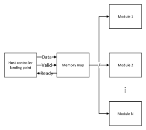
The settings registers are usually considered as an area of memory, in which the stored values represent modes of operation for a design. These stored values are used throughout the design to influence operation. There are a number of ways to achieve the desired behaviour, the seemingly obvious is to simply reference the values, stored in a global memory location, throughout the respective parts of the design, leading to a routing as in Fig. 1.
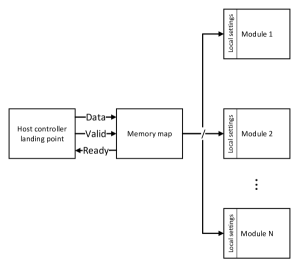
Alternatively, distributing the memory map throughout the design moves the settings closer to where they are used. The result of which is to reduce the complexity of the routing, but not necessarily reduce the overall resource requirement. Local copies of the register map close to the point of which they are used allows the designer to safely register the values into the appropriate clock domains. The additional flip-flop stages play an important part in breaking up the total routed path into smaller elements, the shorter the path, the easier it is for a design to meet timing closure. However, the additional flip-flops used increase the overall resource cost for a design. An example of such a design can be seen in Fig. 2.
Distributing the memory map across the design can be achieved without the need for a increasing the routing complexity. Designing the distributed memory map with a common bus interface for its configuration, Fig. 3, reduces the overall resource cost and significantly reduces the required routing resource.
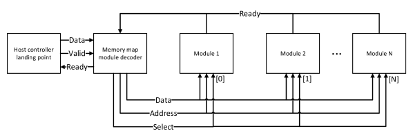
The common bus interface has a number of benefits: reduced routing complexity, safe crossing into different clock domains, reduction in global memory resources, connection into dynamically partially re-configurable logic space.
2.1 Clock domain crossing
It is not uncommon for a modern digital system to use multiple clocks [33], in which data are moved from one clock domain to another and memories are connected to different clock domains. Moving from one clock domain to another requires the use of safe clock domain crossing domains - which in themselves are a large research field [24, 7, 28, 32] - however they require using up yet more valuable resources. Typically configuration data would be set in a slow clock domain and moved into much faster domains - potentially as very wide, parallel busses.
In addition to the increase in resources required for crossing clock domains, multi-clock systems lack determinism which causes problems for the verification process. Rectifying the non-deterministic nature of such systems and providing verification techniques (both stand-alone and built-in) is a rich source of research [37, 23]. Additionally, frameworks for performing timing analyses and signal integrity in a CDC application [28, 32] have been proposed.
The architecture presented here, fig. 3, exports a ‘Ready’ signal from each of the subsystems. The ‘Ready’ signal is used to indicate that the logic has been moved to a safe state in which the local memory map may be written to using the configuration bus. No changes are made to the local configuration memories while logic is operating, hence there is no danger of the registers being sampled while they are transitioning and the clock domains are safely crossed.
2.2 Dynamic partial reconfiguration
Dynamic reconfiguration and Dynamic Partial Reconfiguration (DPR) is rapidly growing in popularity as it enables FPGA designs to be changed at run-time to better meet changing systems demands [25, 11]. The use of DPR is rapidly gaining popularity over a number of sectors including: fault recovery [5], memory controllers [36], real-time signal processing [12], software defined radio [35, 18, 17], cognitive radio [39], bandwidth reduction [30], video filters [20], and RADAR signal processing [41] to name a few.
DPR designs contain a mix of static logic and re-configurable logic. Between the elements of the design a common interconnect is implemented, Fig. 4. The interconnect fabric contains the signals required for the configuration bus. When a module(s) in a re-configurable portion of the FPGA is changed, the configuration bus is connected into the new module along with all other data-path signals. Any settings registers inside partially configured module are then set over the configuration bus.
3 Results
Example designs of the above architectures were written using SystemVerilog (IEEE 1800) and processed using Intel FPGA Quartus Prime 19.1.0 (Build 670); target device for compilation is a Cyclone V (5CSXFC6D6F31C8). Synthesis metrics — Adaptive Logic Modules (ALMs), registers, combinatorial Adaptive Look Up Tables (ALUTs) and maximum operating frequency — are presented for each architecture. Implementations are given for a variety of memory depths and widths.
3.1 Global configuration - no targets
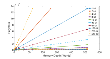
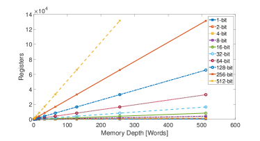
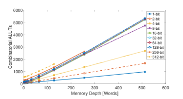
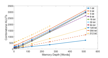
Figures 5 to 8 show key metrics for an implementation of a global memory system. The global memory system contains the decoding logic for writing to the memory, the memory, and the output stage that would be connected to the rest of the design. These figures do not include the resource consumption of slave modules where the settings would be used and any clock domain crossing logic that may be implemented.
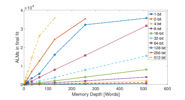
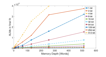
ALMs (Intel) — similar to Configurable Logic Blocks (CLB) (Xilinx) — contain a number of resources, typically (A)LUTs, adders, multiplexers, routing logic, and registers [4]. From fig. 5 it is shown that adding a register stage to the output of the memory significantly increases the number of ALMs needed for implementation; for instance, in this case, 128 512-bit words with a final register stage require just over 10,000 (10,292.6) more ALMs for implementation — approximately an extra 40%. Similarly, the number of dedicated registers (fig. 6) requires an extra 65,536 dedicated logic registers — an approximately 100% increase in resource. Again, the number of ALUTs, fig. 7, has also increased by approximately 40%. This is to be expected since the implementation shown in subfigures (a) of figs. 5 to 8 have an extra register stage per bit of the memory map at the output.
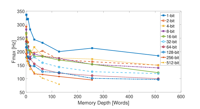
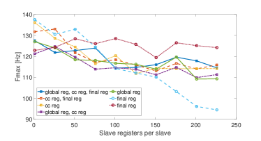
This is an obvious draw back in terms of resource consumption. However, the accompanying benefits of the extra register stage is that the length of the routing between the memory and the target can now be broken down using the extra register stage. This manifests itself in an increase in operating frequency for the design. Figure 8 shows the maximum operating frequency of the implementation that uses an extra register. While synthesising just the memory module itself we are unable to provide figures when there is no additional output register because there are no valid paths (paths between two flip-flops) for which the timing analyzer (TimeQuest) can operate.
3.2 Global configuration with targets
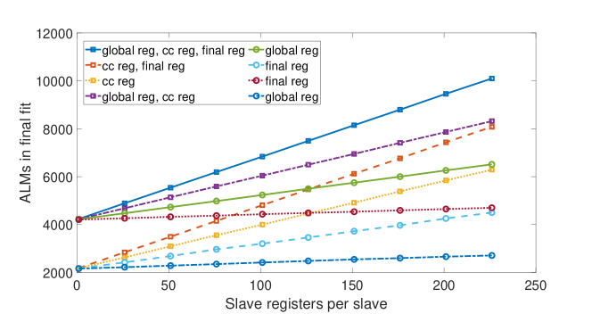
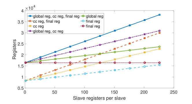
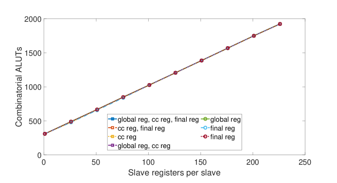
In sect. 3.1 the resource consumption for the memory decode logic and memory itself are shown. However, this is only half the story for a design that uses a global set of memory where entries are propagated out to other areas of the design. In this section we take a global memory system that a global memory of 256 32-bit words and propagates these out to a slave module with a varying number of configuration registers in the slave module. In addition, designs that use a combination of output registers on the global memory map, clock domain crossing registers (synchronisation chain length is 2 registers) and final location registers are examined.
Figure 9 is the after fitting ALM requirements, fig. 10 is the after fitting register requirements, and fig. 11 is the after fitting ALUT requirements for each configuration of the global memory map architecture. As is expected, increasing the number of target registers linearly increases the requirement of each resource. Designs with a greater number of register stages (post global map register, clock domain crossing synchronisation chain registers and destination registers) significantly increases the resource requirements compared to design with fewer register stages. 10099.1 ALMs, 38146 registers, and 1925 ALUTs for a design with 226 configuration registers and the maximum number of routing register stages compared to 2710.5 ALMs, 8258 registers, and 1913 ALUTs for a design with the same number of configuration registers but no register stages to break down the length of the routing. The more crowded a design becomes, the greater the impact of removing the routing registers has on the maximum speed of a path.
3.3 Distributed configuration
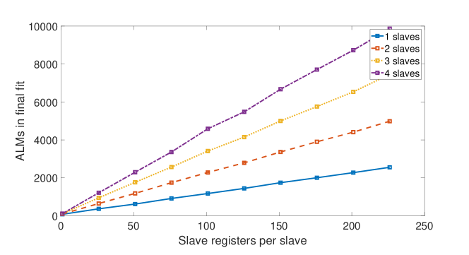
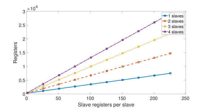
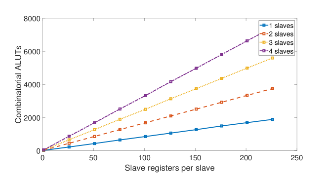
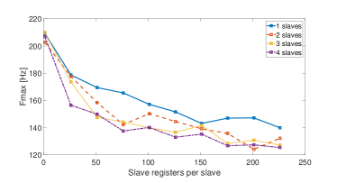
The resources required for the distributed configuration memory architecture, shown in figs. 12 to 14 are considerably lower than the global memory architecture. The graphs shown here are for implementations with a number of slave modules (1 to 4) each implementation varies the number of configurations per slave. For comparisons numbers from the ‘1 slave’ implementations can be mapped to the results given in sect. 3.2.
The resources used for a distributed configuration memory implementation using 226 target registers per slave are: 2556.0 ALMs, 7499 registers, and 1887 ALUTs. That is 25% of the ALMs, 20% of the registers used in the global design with maximum routing register. A significant cost saving. Increasing the number of slaves in the design has a linear effect on the resource cost.
3.4 Operating frequency
Figure 15 shows that the maximum operating frequency of a design is also influenced by the topology of the configuration architecture. A global memory architecture achieves a maximum of just shy of 140 MHz compared to the approximate 210 MHz of the distributed memory architecture.
4 Conclusions
In this paper it has been shown that there are a number of ways to achieve the implementation of configuration registers in an FPGA design. In this paper we proposed a global memory architecture and a distributed memory architecture, for completeness the global memory architecture was presented with combinations of register stages and clock domain crossing registers. It has been shown that the distributed architecture has a much lower resource cost for ALMs and registers (as small as 25% and 20% respectively for a design using 226 32-bit configuration registers). It has further been shown that there is a disparity in the maximum operating frequency between the designs with the distributed memory architecture achieving a higher maximum operating frequency.
Aside from the reduction in resource cost between the different architectures, the distributed memory architecture uses a common configuration bus that is independent of the number of target registers and their width. The uniformity of the configuration bus opens up the ability to implement the configuration system in a partially re-configurable FPGA design, where the configuration bus can be connected to any re-configurable design without penalty. Similarly, the architecture of the configuration bus is not liable to mis-sampling when crossing clock domains. It is set only when the slave module reports it is safe to change the settings.
References
- [1] AN 903: Accelerating timing closure: in Intel Quartus Prime Pro Edition. https://www.intel.com/content/www/us/en/programmable/documentation/fcv1571168848135.html. Accessed: 2020-19-03.
- [2] Verilog parameters. http://verilog.renerta.com/mobile/source/vrg00032.htm. Accessed: 2020-19-03.
- [3] VHDL generics. http://vhdl.renerta.com/mobile/source/vhd00034.htm. Accessed: 2020-19-03.
- [4] Altera white paper FPGA architecture. https://www.intel.com/content/dam/www/programmable/us/en/pdfs/literature/wp/wp-01003.pdf, 2006. Accessed: 2020-19-03.
- [5] G. I. Alkady, N. A. El-Araby, M. B. Abdelhalim, H. H. Amer, and A. H. Madian. Dynamic fault recovery using partial reconfiguration for highly reliable fpgas. In 2015 4th Mediterranean Conference on Embedded Computing (MECO), pages 56–59, June 2015.
- [6] A. Azad and A. Buluç. Distributed-memory algorithms for maximum cardinality matching in bipartite graphs. In 2016 IEEE International Parallel and Distributed Processing Symposium (IPDPS), pages 32–42, May 2016.
- [7] M. Bartik. Clock domain crossing — an advanced course for future digital design engineers. In 2018 7th Mediterranean Conference on Embedded Computing (MECO), pages 1–5, June 2018.
- [8] G. Cordasco, V. Scarano, and A. L. Rosenberg. Bounded-collision memory-mapping schemes for data structures with applications to parallel memories. IEEE Transactions on Parallel and Distributed Systems, 18(7):973–982, July 2007.
- [9] A. Darte and Y. Robert. Communication-minimal mapping of uniform loop nests onto distributed memory architectures. In Proceedings of International Conference on Application Specific Array Processors (ASAP ’93), pages 1–14, Oct 1993.
- [10] Greg Daughtry. Top 5 timing closure techniques. https://www.xilinx.com/publications/prod_mktg/club_vivado/presentation-2015/paris/Xilinx-TimingClosure.pdf. Accessed: 2020-19-03.
- [11] X. Di, S. Fazhuang, D. Zhantao, and H. Wei. A design flow for fpga partial dynamic reconfiguration. In 2012 Second International Conference on Instrumentation, Measurement, Computer, Communication and Control, pages 119–123, Dec 2012.
- [12] M. Feilen, M. Ihmig, A. Zahlheimer, and W. Stechele. Real-time signal processing on low-cost-fpgas using dynamic partial reconfiguration. In 2011 International Symposium on Integrated Circuits, pages 110–113, Dec 2011.
- [13] Feng Huang and J. Bacon. Operating system support for flexible coherence in distributed shared memory. In Proceedings of HICSS-29: 29th Hawaii International Conference on System Sciences, volume 1, pages 92–101 vol.1, Jan 1996.
- [14] Christian Fobel, Gary Gréwal, and Andrew Morton. Hardware accelerated fpga placement. Microelectron. J., 40(11):1667–1671, November 2009.
- [15] V. G. Gudise and G. K. Venayagamoorthy. Fpga placement and routing using particle swarm optimization. In IEEE Computer Society Annual Symposium on VLSI, pages 307–308, Feb 2004.
- [16] Malay Haldar, Anshuman Nayak, Alok Choudhary, and Prith Banerjee. Parallel algorithms for fpga placement. In Proceedings of the 10th Great Lakes Symposium on VLSI, GLSVLSI ’00, page 86–94, New York, NY, USA, 2000. Association for Computing Machinery.
- [17] A. Hassan, R. Ahmed, H. Mostafa, H. A. H. Fahmy, and A. Hussien. Performance evaluation of dynamic partial reconfiguration techniques for software defined radio implementation on fpga. In 2015 IEEE International Conference on Electronics, Circuits, and Systems (ICECS), pages 183–186, Dec 2015.
- [18] S. Hosny, E. Elnader, M. Gamal, A. Hussien, A. H. Khalil, and H. Mostafa. A software defined radio transceiver based on dynamic partial reconfiguration. In 2018 New Generation of CAS (NGCAS), pages 158–161, Nov 2018.
- [19] Jong Hyuk Choi and Kyu Ho Park. Hybrid full map directory scheme for distributed shared memory multiprocessors. In Proceedings High Performance Computing on the Information Superhighway. HPC Asia ’97, pages 30–34, April 1997.
- [20] R. Khraisha and J. Lee. A scalable h.264/avc deblocking filter architecture using dynamic partial reconfiguration. In 2010 IEEE International Conference on Acoustics, Speech and Signal Processing, pages 1566–1569, March 2010.
- [21] F. Klein, K. Beineke, and M. Schöttner. Memory management for billions of small objects in a distributed in-memory storage. In 2014 IEEE International Conference on Cluster Computing (CLUSTER), pages 113–122, Sep. 2014.
- [22] L. I. Kontothanassis and M. L. Scott. Using memory-mapped network interfaces to improve the performance of distributed shared memory. In Proceedings. Second International Symposium on High-Performance Computer Architecture, pages 166–177, Feb 1996.
- [23] C. Leong, P. Machado, V. Bexiga, J. P. Teixeira, I. C. Teixeira, J. C. Silva, P. Lousã, and J. Varela. Built-in clock domain crossing (cdc) test and diagnosis in gals systems. In 13th IEEE Symposium on Design and Diagnostics of Electronic Circuits and Systems, pages 72–77, April 2010.
- [24] Y. Li, B. Nelson, and M. Wirthlin. Synchronization techniques for crossing multiple clock domains in fpga-based tmr circuits. IEEE Transactions on Nuclear Science, 57(6):3506–3514, Dec 2010.
- [25] W. Lie and W. Feng-yan. Dynamic partial reconfiguration in fpgas. In 2009 Third International Symposium on Intelligent Information Technology Application, volume 2, pages 445–448, Nov 2009.
- [26] Z. Lin, D. H. P. Chau, and U. Kang. Leveraging memory mapping for fast and scalable graph computation on a pc. In 2013 IEEE International Conference on Big Data, pages 95–98, Oct 2013.
- [27] V. M. Lo. Temporal communication graphs: A new graph theoretic model mapping and scheduling in distributed memory systems. In The Sixth Distributed Memory Computing Conference, 1991. Proceedings, pages 248–252, April 1991.
- [28] A. Matsuda and Jin Zhang. Debugging methodology and timing analysis in cdc solution. In 2011 9th IEEE International Conference on ASIC, pages 365–368, Oct 2011.
- [29] C. Mulpuri and S. Hauck. Runtime and quality tradeoffs in fpga placement and routing. In FPGA ’01: Proceedings of the 2001 ACM/SIGDA ninth international symposium on Field programmable gate arrays, pages 29–36, Feb 2001.
- [30] S. M. Najmabadi, Z. Wang, Y. Baroud, and S. Simon. Online bandwidth reduction using dynamic partial reconfiguration. In 2016 IEEE 24th Annual International Symposium on Field-Programmable Custom Computing Machines (FCCM), pages 168–171, May 2016.
- [31] A. Pal and M. Balakrishnan. A behavioral synthesis approach for distributed memory fpga architectures. In 2007 International Conference on Field Programmable Logic and Applications, pages 517–520, Aug 2007.
- [32] I. N. Preetam, P. Mazumder, T. S. Kumar, S. R. Krishna, and R. Kumawat. Design and verification of ethernet, vme ip core using ace and cdc. In 2015 2nd International Conference on Electronics and Communication Systems (ICECS), pages 194–198, Feb 2015.
- [33] O. Ragheb and J. H. Anderson. High-level synthesis of fpga circuits with multiple clock domains. In 2018 IEEE 26th Annual International Symposium on Field-Programmable Custom Computing Machines (FCCM), pages 109–116, April 2018.
- [34] J. H. Rutgers, M. J. G. Bekooij, and G. J. M. Smit. Portable memory consistency for software managed distributed memory in many-core soc. In 2013 IEEE International Symposium on Parallel Distributed Processing, Workshops and Phd Forum, pages 212–221, May 2013.
- [35] A. Sadek, H. Mostafa, and A. Nassar. On the use of dynamic partial reconfiguration for multi-band/multi-standard software defined radio. In 2015 IEEE International Conference on Electronics, Circuits, and Systems (ICECS), pages 498–499, Dec 2015.
- [36] K. Salah. An area efficient multi-mode memory controller based on dynamic partial reconfiguration. In 2017 8th IEEE Annual Information Technology, Electronics and Mobile Communication Conference (IEMCON), pages 328–331, Oct 2017.
- [37] M. Su, Y. Chen, and X. Gao. A general method to make multi-clock system deterministic. In 2010 Design, Automation Test in Europe Conference Exhibition (DATE 2010), pages 1480–1485, March 2010.
- [38] H. Tirri and S. Mallenius. Optimizing the hard address distribution for sparse distributed memories. In Proceedings of ICNN’95 - International Conference on Neural Networks, volume 4, pages 1966–1970 vol.4, Nov 1995.
- [39] Wang Lie and Wu Feng-yan. Dynamic partial reconfiguration on cognitive radio platform. In 2009 IEEE International Conference on Intelligent Computing and Intelligent Systems, volume 4, pages 381–384, Nov 2009.
- [40] Michael G. Wrighton and André M. DeHon. Hardware-assisted simulated annealing with application for fast fpga placement. In Proceedings of the 2003 ACM/SIGDA Eleventh International Symposium on Field Programmable Gate Arrays, FPGA ’03, page 33–42, New York, NY, USA, 2003. Association for Computing Machinery.
- [41] Y. Zhang, Z. Wang, and J. Wang. Integrated radar signal processing using fpga dynamic reconfiguration. In 2016 CIE International Conference on Radar (RADAR), pages 1–4, Oct 2016.