∎
3 Purdue Center for Predictive Materials and Devices, Purdue University, West Lafayette, IN 47907, USA
4 Purdue Institute of Inflammation, Immunology and Infectious Disease, Purdue University, West Lafayette, IN 47907, USA
Mode-space-compatible inelastic scattering in atomistic nonequilibrium Green’s function implementations
Abstract
The nonequilibrium Green’s function (NEGF) method is often used to predict transport in atomistically resolved nanodevices and yields an immense numerical load when inelastic scattering on phonons is included. To ease this load, this work extends the atomistic mode space approach of Ref. Milnikov2012 to include inelastic scattering on optical and acoustic phonons in silicon nanowires. This work also includes the exact calculation of the real part of retarded scattering self-energies in the reduced basis representation using the Kramers-Kronig relations. The inclusion of the Kramers-Kronig relation for the real part of the retarded scattering self-energy increases the impact of scattering. Virtually perfect agreement with results of the original representation is achieved with matrix rank reductions of more than 97%. Time-to-solution improvements of more than 200 and peak memory reductions of more than 7 are shown. This allows for the solution of electron transport scattered on phonons in atomically resolved nanowires with cross-sections larger than 5 nm 5 nm.
Keywords:
Nanoelectronics NEGF Low-rank approximations Inelastic scattering Mode space1 Introduction
The characteristic length scale of state-of-the-art logic devices has reached dimensions with a countable number of atoms Charles2016 ; itrs . At this scale, quantum effects such as tunneling, interference and confinement drastically change device performance pierret1996semiconductor ; datta2005quantum ; Ciraci2001 ; Jing . Understanding and optimizing these effects almost always requires predictive models. The nonequilibrium Green’s function (NEGF) formalism is a well-accepted model for coherent and incoherent electron transport in nanodevices Datta2000 ; Luisier2006 .
Characteristic nanoelectronic device dimensions contain a countable number of atoms, but a typical transistor contains hundreds to thousands of atoms in the volume of only a few cubic nanometers. Accurate basis representations such as the empirical tight binding method boykin1991tight ; Tan2015 usually contain tens of matrix elements per atom representing atomic orbitals luisier2006atomistic . Solving the NEGF equations in a tight binding basis can be computationally cumbersome due to the required matrices consisting of thousands of rows and columns Bermeo2015 ; afzalian2015mode ; guo2005nano . To ease this numerical load, the recursive Green’s function method (RGF) Lake1997 provides a block-wise recursive solution for NEGF equations that can be discretized with block-tridiagonal sparse matrices Afzalian2017 ; chen2015approximate ; kuzmin2013fast . In that case, NEGF has been solved for nanodevices represented in realistic basis sets valencia2016grain ; Wang2017 ; ilatikhameneh2015tunnel ; chen2015nemo5 . With RGF, computational complexity depends on the cross-section and length of the device. In a typical nanowire device, the size of the blocks solved with the RGF method is directly proportional to the degrees of freedom in the cross-section of the device. Time-to-solution of matrix operations on these blocks scales on the order of . Memory scales on the order of .
The NEGF equations must be self-consistently solved with the Poisson equation that represents the electrostatic effects caused by the quantum mechanical evolution of the system Datta2000 ; datta2002non ; trellakis1997iteration . This introduces a degree of complexity to the solution of NEGF, since solving the equations is required multiple times.
An advantage of the NEGF and RGF methods is the ability to introduce incoherent scattering through self-energies, which represent device structure uncertainties such as roughness, alloy disorder and geometric errors, and temperature fluctuations through phonons Datta2000 ; Kubis2011 ; he2012efficient ; anantram2008modeling ; Sarangapani2019 ; Zhang2010 ; Nguyen2013 ; Aldegunde2013 ; Valin2014 ; He2014 ; Ramayya2008 . However, the introduction of incoherent scattering into the RGF solution introduces yet another degree of complexity through the self-consistent solution of retarded () and lesser () Green’s functions. Their equations read symbolically
| (1) |
| (2) |
and the respective scattering self-energies
| (3) |
| (4) |
In the above equations, is the electronic Hamiltonian, is an identity matrix, and is the electronic energy for which the Green’s functions and self-energies are being solved. is the sum of environmental Green’s functions with phonon, impurity and roughness information kubis2009theory ; Kubis2011 . Within the self-consistent Born approximation the scattering self-energies and Green’s functions are solved iteratively to achieve particle number conservation Kubis2011 ; kubis2009quantum ; Luisier2010 . It is worth mentioning that some alternatives to the self-consistent Born approximation of scattering exist, such as low-order approximations Lee2017 ; Lee2016 ; Mera2012 , the Büttiker probe scattering model Datta2000 ; Miao2016 ; Chu2019 and the multi-scale approach of Ref. Geng2018 . Although these methods are compatible with the mode space approach, they are beyond the scope of this work.
Many discretized degrees of freedom are common in atomistic representations, as well as the two layers of self-consistency, and usually result in heavy computational burdens. To ease this burden, incoherent scattering effects are often neglected in NEGF transport calculations datta2005quantum ; venugopal2003simple ; mamaluy2003efficient ; rahman2003theory ; shao2005nanoscale . In the case of atomistic representations, even ballistic NEGF calculations often yield large computational loads. Such situations have motivated the introduction of a low rank approximation markovsky2011low into NEGF chen2015approximate ; mamaluy2003efficient ; Zeng2013 ; hetmaniuk2015reduced ; birner2009ballistic ; he2012efficient , which is often called the mode space approach afzalian2015mode ; Afzalian2017 ; venugopal2003simple ; Huang2017 . Since scattering phenomena are important to retain in quantum transport simulations, the goal of this work is to introduce a low rank approximation that accurately retains scattering phenomena and is still based on an atomistic device representation.
2 Method
2.1 Mode space approach in tight binding
Low-rank approximations such as the mode space method afzalian2015mode ; Zeng2013 ; Huang2017 follow a common process: The system’s Hamiltonian is transformed into a basis representation that allows for filtering of degrees of freedom that are unlikely to contribute to device operation. This reduces the rank of the system’s Hamiltonian and thus the complexity of the NEGF equations. Choosing the eigenvectors of the Hamiltonian according to their eigen-energies often provides a good measure of filtering empty states Milnikov2012 ; birner2009ballistic . Unfortunately, this direct filtering fails in tight binding due to the appearance of spurious states Milnikov2012 ; Huang2017 . The method developed by Mil’nikov et al. Milnikov2012 removes these spurious states.
For completeness we repeat this method here: The first step of the method is to obtain the eigenvectors within the desired energy interval . The original basis Hamiltonian is transformed to a lower rank (mode space) basis using a rectangular transformation matrix constructed from the eigenvectors :
| (5) |
At this stage, the reduced Hamiltonian yields several unphysical states. A modified reduced Hamiltonian is created by adding new orthogonal basis states () such that
| (6) |
where
| (7) |
The added states do not deteriorate the basis and have no effect on non-spurious states. The purpose of the added state is to remove the spurious states, thus are chosen such that they reduce the number of spurious states in the band structure. Since adding states to the basis keeps the physics unaltered Milnikov2012 , states are added until all spurious states within the energy interval are removed and a transformation matrix is produced. The method by Mil’nikov et al. is therefore a minimization problem Milnikov2012 . Although devices in this work are homogeneous, and only require one basis to transform all portions of the nanowire, a heterogeneous device of varying cross-sections or materials may be transformed by use of multiple basis transformation matrices . It is therefore possible to introduce explicit defects such as roughness and impurities when is obtained with such defects.
2.2 Mode generation in NEMO5
In this work, the mode space basis states are determined by following Mil’nikov et al. Milnikov2012 with the ModeSpace solver Huang2017 of the multipurpose nanodevice simulation tool NEMO5 Steiger2011 ; nemo5 . Details of this algorithm can be found in Refs. Milnikov2012 and Huang2017 . Ratios of the reduced and original Matrix ranks are regularly achieved with this NEMO5 solver while the transport physics are preserved afzalian2015mode ; Huang2017 . This has enabled speedups for ballistic NEGF simulations of up to 10,000 times Afzalian2017 .
2.3 Expanding atomistic mode space to incoherent scattering simulations
In this work, this method is augmented to handle incoherent scattering that allows for intermode transitions. Scattering self-energies for the scattering of electrons on phonons are originally defined in a real space representation. Electron scattering on acoustic and optical phonons via deformation potentials is considered following Ref. Charles2016 (cf. Eqs. 1-6 of Ref. Charles2016 ). Calculations in polar materials (such as InAs) include scattering of electrons on polar optical phonons as well Riddoch1983 . Since these self-energies are formulated in real space and require position information, an issue arises as this information is no longer directly available after a mode space basis transformation.
2.4 Form factor transformation
To make position information available for the solution of scattering self-energies while limiting the number of transformations, a form factor is introduced. This form factor is fully explained by Ref. Afzalian2011 . The form factor contains all modes involved in the respective scattering process:
| (8) |
where ,,, are indices of the real modes (columns) of the transformation matrix . The index is iterated through the rows of . We define each element of and of Eqs. 4-6 of Ref. Charles2016 as and each element of a Green’s function matrix as . We also define as the product of all scalar factors involved in each of the Eqs. 4-6 of Ref. Charles2016 . The form factor elements are applied to the Green’s function elements as follows:
| (9) |
In this way, all matrices remain in mode space.
2.5 Approximation of form factor
The form factor is four-dimensional and scales rapidly with the number of modes in terms of memory (), time for construction () and time for application (). This can easily result in the form factor construction taking a significant amount of time and memory and application taking a significant amount of time. Similarly to Ref. Afzalian2011 , we have observed that eliminating off-diagonal elements of the form factor , such that for and , provides reasonable physical results. This approximation corresponds to the lack of interaction between modes which are uncoupled in real space. Therefore, no inter-mode scattering takes place when the form factor is diagonal. This does not restrict inelastic scattering, since the electronic energy is a mode-independent parameter. This approximation provides a memory-thin form factor with memory scaling on the order of . The construction complexity of the form factor is also reduced to , while the application complexity is reduced to . Note that although this yields an accurate calculation of self-energies and , mode coupling terms ( for ) must remain for an accurate calculation of electron density Afzalian2011 .
2.6 Inclusion of real part of retarded scattering self-energies using Kramers-Kronig relations
The general form of the retarded scattering self-energy includes a principal value integral of large computational burden Milnikov2012 ; Charles2016 ; Frey ; Esposito2009 ; Svizhenko2003 ; Wacker2002 . can be obtained by its separate real and imaginary parts Frey ; Esposito2009 ; Svizhenko2003 such that
| (10) |
Typically, the real part of the retarded self-energy is entirely excluded, and although the approximation often yields reasonable physical results Milnikov2012 ; Svizhenko2003 , it is known that excluding the real part causes deviations. In particular, off-state current densities are underestimated in this approximation Charles2016 ; Frey ; Esposito2009 . Note that the real part of retarded self-energies shifts resonance energies and thus influences band edges and threshold voltages kubis2009quantum . In this work, the exact real part of the retarded scattering self-energies is obtained using the Kramers-Kronig relations Kronig1925 . For each matrix element of a retarded self-energy, its real part is obtained by applying the Kramers-Kronig relation on its imaginary part . Using a Hilbert transform , the real part becomes:
| (11) |
This Hilbert transform is performed using a fast Fourier transform (FFT), a multiplication in the Fourier space, and an inverse FFT afterwards Cizek1970 .
3 Results and discussion
3.1 Simulation setup
To ensure the validity of the presented low-rank approximation for transport in nanowire devices including inelastic scattering, multiple tests were performed with NEMO5 Steiger2011 ; fonseca2013efficient ; sellier2012nemo5 . First, for validation, results of simulations in a mode space basis were benchmarked against calculations in the original tight binding basis. These result comparisons are shown in Sec. 3.2. Second, multiple performance tests comparing time-to-solution and peak memory improvements in mode space are shown in Sec. 3.3 for various device widths w. The device used for both validation and performance tests was a w w 20.65 nm silicon nanowire as shown in Fig. 1, where w is the variable width in nm of the square cross-section of the device. The device had a 1 nm gate oxide layer surrounding the central region. The original basis was a 10-band tight binding model using the parameter set of Ref. boykin2004valence . A source-drain bias of 0.2 V was applied to the device. Note that the applied source-drain bias does not affect the validity of the presented method, and mode space calculations with higher source-drain voltages can be found in Refs. Afzalian2017 ; Huang2017 ; Afzalian2018 . The device was NIN doped, with the 5.97 nm source and 6.66 nm drain regions having a cm-3 doping density and the central 8.02 nm intrinsic region having a cm-3 doping density. The lengths , and are labeled in Fig. 1. Simulations of Si devices included both inelastic optical phonon and elastic acoustic phonon deformation potential scattering, applied to the NEGF equations through self-energies in the self-consistent Born approximation Charles2016 ; anantram2008modeling . For polar materials, scattering on polar optical phonons was included as well. The inhomogeneous energy grid was generated using an adaptive grid generator in NEMO5 Charles2016 . Due to the high numerical load of the Kramers-Kronig relation for scattering in tight binding representations, the real parts of all scattering self-energies in the benchmarking scenarios of Secs. 3.2, 3.3 and 3.4 were neglected. This is not the case in Sec. 3.5, where a non-zero real part of the scattering self-energy will be included.
An assessment of the real part of the retarded self-energies was done by comparison of the resulting current-voltage (I-V) characteristics shown in Sec. 3.5. For this assessment, the material of the transistor in Fig. 1 was chosen to be InAs, with two tested device widths 2.42 nm and 3.63 nm. Both devices had an 5.97 nm p-type source doped at cm-3, an n-type 9.66 nm drain doped at cm-3 and a 14.66 nm central undoped region. A source-drain bias of 0.3 V was applied. Since TFETs require the occupation of both electrons and holes, the method of Ref. Milnikov2012 was applied to obtain modes for a wide energy window that included bands near the conduction and valence band edges. The inclusion of holes also necessitates a proper definition of electrons and holes as states tunnel from valence band to conduction band in the TFET. An interpolation method was applied as defined by Ref. Charles2016 to avoid sharp transitions from holes to electrons or vice versa. Simulations included optical phonon, acoustic phonon and polar-optical phonon scattering to represent the polar nature of InAs. Due to the non-local nature of polar-optical phonon scattering, such a calculation would be very expensive even in a reduced basis. To avoid this, a local scattering calculation was performed using a cross-section-dependent compensation factor defined in Ref. Sarangapani2019 . Compensating scaling factors of 30.0 and 26.56 were used in the calculation of polar-optical phonon scattering for the 2.42 nm and 3.63 nm devices respectively. Note, the form factor approximation as described in Sec. 2.5 was not performed in this case.

3.2 Validation of mode space simulation results
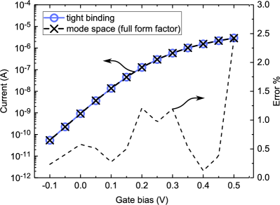
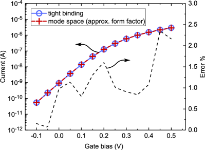
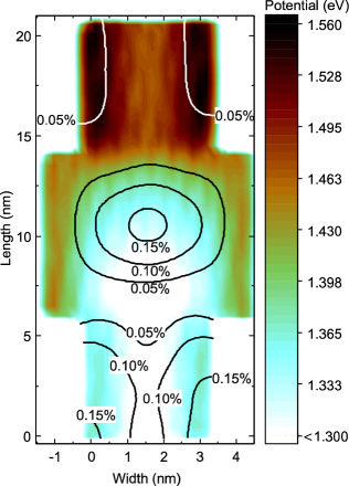
For validation, a silicon nanowire of width w nm was used (see Fig. 1). The mode space simulation had a reduction ratio of 2.8%, transforming matrix blocks from 2880 2880 matrices to 81 81 matrices. NEGF was solved using the scattering-compatible RGF algorithm anantram2008modeling . Fig. 2 shows the current-voltage (I-V) characteristic curves of both the original tight binding basis and mode space basis for sweeping gate biases ranging from -0.1 V to 0.5 V. The mode space scattering results of Fig. 2 were obtained using the full form factor as described in Sec. 2.4. The virtually identical results of mode space and tight binding show that the mode space low-rank approximation provides a valid and highly efficient model for quantum transport simulations with inelastic scattering. Fig. 3 shows that the mode space approach with approximate form factors, as discussed in Sec. 2.5, also yields results very close to those of the original basis calculations. Fig. 4 shows a contour plot of the potential profile of the center cross-section of the device for a tight binding simulation at the applied gate bias of 0.5 V. Contour lines show the relative error of the mode space potential profile results relative to the original tight binding data. Note that the mode space method agrees with NEGF calculations in the original tight binding representation for many wire cross-sections as similarly well as those shown in Figs. 2 and 3. Similar benchmark data can be found in Refs. Milnikov2012 ; Huang2017 ; Afzalian2018 .
3.3 Assessment of computational performance
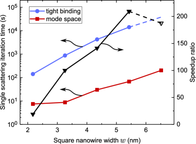
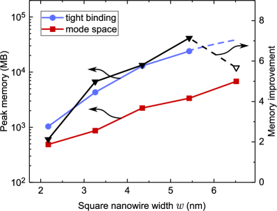
The device in Fig. 1 was used with varying widths w to measure performance improvements in NEMO5 time-to-solution and peak memory. Each width also had a corresponding mode space transformation matrix with its respective number of modes. Correspondingly, the reduction ratios in Figs. 5 and 6 vary. The exact width values simulated were 4, 6, 8, 10 and 12 silicon unit cells and the respective reduction ratios were 5.6%, 2.8%, 2.9%, 2.8% and 3.0%. The lattice parameter of silicon was assumed to be 0.54 nm. All performance simulations were performed with the same inputs of Sec. 3.2, with the exception that a fixed number of 256 energies was used. Since results for the approximate form factor have been shown in Fig. 3 to closely match those of the full form factor, mode space data for performance comparisons in this section were generated using the approximate form factor. The Green’s functions were solved for 256 energies with 1 energy per MPI process. Each MPI process was designated to a 32-core node on the Blue Waters petascale supercomputer at the University of Illinois at Urbana-Champaign bluewaters . Each MPI process was assigned 32 OpenMP threads for multithreaded matrix operations and form factor construction and application. Fig. 5 shows the average time (of 6 iterations) to compute a single self-consistent Born iteration. Each self-consistent Born iteration includes the time to compute the RGF algorithm as well as the time to compute lesser scattering self-energies and retarded scattering self-energies for optical and acoustic deformation potential inelastic scattering. The calculation of scattering self-energies involves a large degree of communication between MPI processes as discussed in Ref. Charles2016 .
The timing shown does not include the calculation of other aspects of quantum transport such as the solution of the Poisson’s equation and the generation of the adaptive energy grid. This exclusion of such calculations can be justified by the fact that the time-to-solution is negligible when compared to the solution of NEGF. In production runs, those calculations are performed only a small fraction of times when compared to the multiple self-consistent Born iterations per Poisson iteration. The maximum speedup obtained with low-rank approximations for an iteration in this work was of 209.5 times. Due to computational limitations, the tight binding simulation for the point w 6.52 nm was not assessed, since a single iteration would have taken about 38,000 seconds according to a power fitting function of the existing data. By extrapolating the data, the speedup for w 6.52 nm is predicted to be of 187.5 times, as is shown in Fig. 5. It can be noted that this is lower than the speedup of w 5.43 nm. This is likely due to the fact that the reduction ratio for w 6.52 nm is slightly higher at 3.0% than for w 5.43 nm at 2.8%. Fig. 6 shows the peak memory of the same simulations run for Fig. 5. The maximum peak memory reduction was of 7.14. Similarly to Fig. 5, a power fitting function was used to predict the peak memory for a device of w 6.52 nm, which results in a predicted peak memory reduction of 5.67.
3.4 Simulating beyond existing capabilities
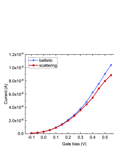
With the time-to-solution and memory footprint significantly reduced, the opportunity to simulate larger devices with complex physical phenomena such as incoherent scattering of multiple types (phonons, roughness, impurities) is now accessible. Ref. Charles2016 describes the simulation of a circular nanowire, with acoustic and optical deformation potential scattering and a 10-band tight binding basis. The diameter of the cross-section of this device was 3 nm, and the device length was 27 nm. Solution of an I-V characteristic curve took approximately 275 hours on 330 cores on the Blue Waters petascale supercomputer. The peak memory was 60 GB per node, which is close to the maximum node memory of 64 GB. This device therefore approaches the limit of what can be simulated in a full basis representation such as tight binding. To demonstrate the capability of solving larger devices in a reduced basis, a full I-V curve was generated for a square nanowire of Fig. 1 with w 5.43. Due to the different cross-sectional geometry this nanowire has over 4 times more atoms in the cross-section than the circular nanowire of Ref. Charles2016 . The reduction ratio for the square nanowire was of 2.8%. Fig. 7 shows an I-V characteristic curve for optical and acoustic phonon deformation potential scattering compared to that of a ballistic simulation. As expected, the on-current density is reduced by the inelastic scattering on phonons Charles2016 ; kubis2009theory ; Frey . The scattered transport simulation of the w = 5.43 nm device took approximately 160 total hours on 16,384 cores (2.62 million core hours) on the Blue Waters supercomputer. We estimate that the same I-V calculation would take about 550 million core hours and 168 GB of memory in the original tight binding basis representation.
3.5 Assessment of real part of retarded self-energies
The 2-norms of the real and imaginary parts of the retarded self-energy can show the relative amplitude of their contributions. Comparing the 2-norms of fully charge-self-consistent calculations is misleading, however, since scattering impacts the density of states: The Poisson potential would compensate some of the density of state differences to accommodate the device’s doping profile. Therefore, for this comparison only, scattering self-energies and Green’s functions were solved self-consistently with a fixed Poisson potential. That potential was deduced from a converged ballistic transport solution of the same device. The calculations were performed for the on-state bias of 0.4 V. Table 1 shows the 2-norm values of the real and imaginary parts of the when the Kramers-Kronig relation is observed and when the real part is set to 0. In both of the simulated cross-sections, the norm of the real part is comparable to the norm of the imaginary part. Due to the reduced size of self-energy matrices, it was possible to perform the Hilbert transform on all energies without introducing memory issues and long computation times. Therefore in this work, all energy points generated by the adaptive energy grid in NEMO5 Charles2016 were included in the Hilbert transform of the self-energies.
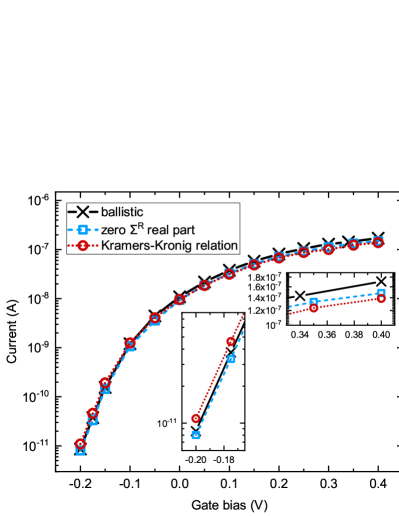
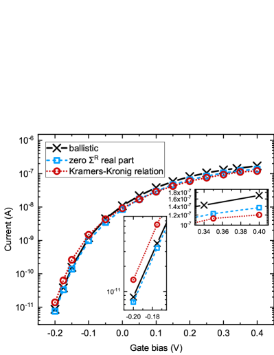
Figs. 8 and 9 show the I-V characteristics of the w = 2.42 nm and w = 3.64 nm devices respectively. Both figures show the differences of the two scattering models (with and without the real part of ) when compared to the ballistic transport. Incoherent scattering increases the off-current density due to scattering-supported gate leakage and decreases the on-current density due to stronger back-scattering. This is in agreement with findings in literature Charles2016 ; Luisier2010 ; Frey ; Svizhenko2003 ; Charles2018 . It should also be noted that the real part of scattering self-energies has notable effects on devices of any dimension, e.g., 1D, 2D and 3D Sarangapani2019 ; Frey . The impact of the real part of becomes more apparent in situations with larger scattering strengths, e.g. when higher temperatures, impurity scattering, or surface roughness scattering are present. Fig. 10 shows the I-V characteristics of the device in Fig. 9 solved with NEGF when all electron-phonon scattering self-energies were multiplied by 2. More significant gate leakage and back-scattering effects can be observed than that shown in Fig. 9. More importantly, however, Fig. 10 shows that the exact with a non-zero real part provides even higher scattering strengths than the approximate, zero real part case. This impact is particularly visible if the charge self-consistency does not compensate deviations from the doping profile. This is exemplified in Fig. 1 of Supplementary Material 1 which shows the charge density in a transistor after a single scattering iteration both in mode space and full tight binding representations. This figure also confirms the physics of the real part of scattering is correctly covered in mode space.
| width w (nm) | zero real | Kramers-Kronig | ||
|---|---|---|---|---|
| real | imag. | real | imag. | |
| 2.42 | 0 | 0.1184 | 0.0965 | 0.1130 |
| 3.64 | 0 | 0.1080 | 0.0920 | 0.1104 |

4 Conclusion
In this work, the atomistic mode space approach of Ref. Milnikov2012 has been augmented to handle inelastic scattering on various types of phonons. The method was verified and benchmarked against results solved in the original representation for silicon nanowires of various sizes. Valid results were achieved with matrix ranks reduced down to 2.8% of their original rank. Time-to-solution was improved by up to 209.5 times, and peak memory was improved by up to 7.14 times. A full I-V calculation was performed in mode space for a 5.43 nm 5.43 nm 20.65 nm silicon nanowire in a tight binding basis, which represents a system size larger than can normally be atomically simulated including inelastic phonon scattering. The solution of the real part of the retarded scattering self-energies with the Kramers-Kronig relations ensures the exact treatment of incoherent scattering. It is demonstrated with calculations of various nanowires that the real part of contributes to transport similarly to the imaginary part. Therefore, a reliable prediction of transport in NEGF must solve for the total complex .
Acknowledgements.
The authors acknowledge financial support by Silvaco Inc. This research is part of the Blue Waters sustained-petascale computing project, which is supported by the National Science Foundation (award number ACI 1238993) and the state of Illinois. Blue Waters is a joint effort of the University of Illinois at Urbana-Champaign and its National Center for Supercomputing Applications. This work is also part of the “Advanced Nanoelectronic Device Design with Atomistic Simulations” PRAC allocation support by the National Science Foundation (award number OCI-1640876). The authors acknowledge the Texas Advanced Computing Center (TACC) at The University of Texas at Austin for providing Stampede2 resources that have contributed to the research results reported within this paper. URL: http://www.tacc.utexas.eduReferences
- [1] Gennady Mil’nikov, Nobuya Mori, and Yoshinari Kamakura. Equivalent transport models in atomistic quantum wires. Physical Review B, 85(3):035317, 2012.
- [2] James Charles, Prasad Sarangapani, Roksana Golizadeh-Mojarad, Robert Andrawis, Daniel Lemus, Xinchen Guo, Daniel Mejia, James E Fonseca, Michael Povolotskyi, Tillmann Kubis, et al. Incoherent transport in nemo5: realistic and efficient scattering on phonons. Journal of Computational Electronics, 15(4):1123–1129, 2016.
- [3] International technology roadmap for semiconductors. https://www.itrs2.net/, 2017. [Online].
- [4] Robert F Pierret. Semiconductor device fundamentals. Pearson Education India, 1996.
- [5] Supriyo Datta. Quantum transport: atom to transistor. Cambridge University Press, 2005.
- [6] S Ciraci, A Buldum, and Inder P Batra. Quantum effects in electrical and thermal transport through nanowires. Journal of Physics: Condensed Matter, 13(29):R537, 2001.
- [7] Guo Jing, Ali Javey, Hongjie Dai, and Mark Lundstorm. Performance analysis and design optimization of near ballistic carbon nanotube field-effect transistors. IEDM Technical Digest. IEEE International Electron Devices Meeting, 2004., pages 703–706, 2004.
- [8] Supriyo Datta. Nanoscale device modeling: the green’s function method. Superlattices and microstructures, 28(4):253–278, 2000.
- [9] Mathieu Luisier, Andreas Schenk, Wolfgang Fichtner, and Gerhard Klimeck. Atomistic simulation of nanowires in the s p 3 d 5 s* tight-binding formalism: From boundary conditions to strain calculations. Physical Review B, 74(20):205323, 2006.
- [10] Timothy B Boykin, Jan PA Van der Wagt, and James S Harris Jr. Tight-binding model for gaas/alas resonant-tunneling diodes. Physical Review B, 43(6):4777, 1991.
- [11] Yaohua P Tan, Michael Povolotskyi, Tillmann Kubis, Timothy B Boykin, and Gerhard Klimeck. Tight-binding analysis of si and gaas ultrathin bodies with subatomic wave-function resolution. Physical Review B, 92(8):085301, 2015.
- [12] Mathieu Luisier, Andreas Schenk, Wolfgang Fichtner, and Gerhard Klimeck. Atomistic simulation of nanowires in the s p 3 d 5 s* tight-binding formalism: From boundary conditions to strain calculations. Physical Review B, 74(20):205323, 2006.
- [13] Robert Andrawis, Jose David Bermeo, James Charles, Jianbin Fang, Jim Fonseca, Yu He, Gerhard Klimeck, Zhengping Jiang, Tillmann Kubis, Daniel Mejia, et al. Nemo5: Achieving high-end internode communication for performance projection beyond moore’s law. arXiv preprint arXiv:1510.04686, 2015.
- [14] Aryan Afzalian, J Huang, H Ilatikhameneh, J Charles, D Lemus, J Bermeo Lopez, S Perez Rubiano, T Kubis, M Povolotskyi, G Klimeck, et al. Mode space tight binding model for ultra-fast simulations of iii-v nanowire mosfets and heterojunction tfets. In Computational Electronics (IWCE), 2015 International Workshop on, pages 1–3. IEEE, 2015.
- [15] Hong Guo. Nano molecular modeling method, April 19 2005. US Patent App. 11/568,103.
- [16] Roger Lake, Gerhard Klimeck, R Chris Bowen, and Dejan Jovanovic. Single and multiband modeling of quantum electron transport through layered semiconductor devices. Journal of Applied Physics, 81(12):7845–7869, 1997.
- [17] Aryan Afzalian, Tim Vasen, Peter Ramvall, and Matthias Passlack. An efficient tight-binding mode-space negf model enabling up to million atoms iii-v nanowire mosfets and tfets simulations. arXiv preprint arXiv:1705.00909, 2017.
- [18] Quan Chen, Jun Li, Chiyung Yam, Yu Zhang, Ngai Wong, and Guanhua Chen. An approximate framework for quantum transport calculation with model order reduction. Journal of Computational Physics, 286:49–61, 2015.
- [19] Andrey Kuzmin, Mathieu Luisier, and Olaf Schenk. Fast methods for computing selected elements of the green’s function in massively parallel nanoelectronic device simulations. In European Conference on Parallel Processing, pages 533–544. Springer, 2013.
- [20] Daniel Valencia, Evan Wilson, Prasad Sarangapani, Gustavo A Valencia-Zapata, Gerhard Klimeck, Michael Povolotskyi, and Zhengping Jiang. Grain boundary resistance in nanoscale copper interconnections. In Simulation of Semiconductor Processes and Devices (SISPAD), 2016 International Conference on, pages 105–108. IEEE, 2016.
- [21] Kuang-Chung Wang, Teodor K Stanev, Daniel Valencia, James Charles, Alex Henning, Vinod K Sangwan, Aritra Lahiri, Daniel Mejia, Prasad Sarangapani, Michael Povolotskyi, et al. Control of interlayer delocalization in 2h transition metal dichalcogenides. arXiv preprint arXiv:1703.02191, 2017.
- [22] Hesameddin Ilatikhameneh, Yaohua Tan, Bozidar Novakovic, Gerhard Klimeck, Rajib Rahman, and Joerg Appenzeller. Tunnel field-effect transistors in 2-d transition metal dichalcogenide materials. IEEE Journal on Exploratory Solid-State Computational Devices and Circuits, 1:12–18, 2015.
- [23] Fan W Chen, Michael Manfra, Gerhard Klimeck, and Tillmann Kubis. Nemo5: Why must we treat topological insulator nanowires atomically? In Proc. IWCE, 2015.
- [24] Supriyo Datta. The non-equilibrium green’s function (negf) formalism: An elementary introduction. In Electron Devices Meeting, 2002. IEDM’02. International, pages 703–706. IEEE, 2002.
- [25] A Trellakis, AT Galick, A Pacelli, and U Ravaioli. Iteration scheme for the solution of the two-dimensional schrödinger-poisson equations in quantum structures. Journal of Applied Physics, 81(12):7880–7884, 1997.
- [26] T Kubis and P Vogl. Assessment of approximations in nonequilibrium green’s function theory. Physical Review B, 83(19):195304, 2011.
- [27] Yu He, Lang Zeng, Tillmann Kubis, Michael Povolotskyi, and Gerhard Klimeck. Efficient solution algorithm of non-equilibrium green’s functions in atomistic tight binding representation. In Proc. 15th Int. Workshop Comput. Electron, pages 1–3, 2012.
- [28] MP Anantram, Mark S Lundstrom, and Dmitri E Nikonov. Modeling of nanoscale devices. Proceedings of the IEEE, 96(9):1511–1550, 2008.
- [29] Prasad Sarangapani, Yuanchen Chu, James Charles, Gerhard Klimeck, and Tillmann Kubis. Band-tail Formation and Band-gap Narrowing Driven by Polar Optical Phonons and Charged Impurities in Atomically Resolved III-V Semiconductors and Nanodevices. Physical Review Applied, 12(4):1, 2019.
- [30] Wenxing Zhang, Christophe Delerue, Yann Michel Niquet, Guy Allan, and Enge Wang. Atomistic modeling of electron-phonon coupling and transport properties in n -type [110] silicon nanowires. Physical Review B - Condensed Matter and Materials Physics, 82(11):2–8, 2010.
- [31] Viet Hung Nguyen, François Triozon, Frédéric D.R. Bonnet, and Yann Michel Niquet. Performances of strained nanowire devices: Ballistic versus scattering-limited currents. IEEE Transactions on Electron Devices, 60(5):1506–1513, 2013.
- [32] M. Aldegunde, A. Martinez, and J. R. Barker. Study of individual phonon scattering mechanisms and the validity of Matthiessen’s rule in a gate-all-around silicon nanowire transistor. Journal of Applied Physics, 113(1), 2013.
- [33] R. Valin, M. Aldegunde, A. Martinez, and J. R. Barker. Quantum transport of a nanowire field-effect transistor with complex phonon self-energy. Journal of Applied Physics, 116(8), 2014.
- [34] Yu He, Yu Wang, Gerhard Klimeck, and Tillmann Kubis. Non-equilibrium Green’s functions method: Non-trivial and disordered leads. Applied Physics Letters, 105(21), 2014.
- [35] E. B. Ramayya, D. Vasileska, S. M. Goodnick, and I. Knezevic. Electron transport in silicon nanowires: The role of acoustic phonon confinement and surface roughness scattering. Journal of Applied Physics, 104(6), 2008.
- [36] T Kubis, C Yeh, P Vogl, A Benz, G Fasching, and C Deutsch. Theory of nonequilibrium quantum transport and energy dissipation in terahertz quantum cascade lasers. Physical Review B, 79(19):195323, 2009.
- [37] Tillmann Christoph Kubis. Quantum transport in semiconductor nanostructures. PhD thesis, Technical University of Munich, 2009.
- [38] Mathieu Luisier and Gerhard Klimeck. Simulation of nanowire tunneling transistors: From the wentzel–kramers–brillouin approximation to full-band phonon-assisted tunneling. Journal of Applied Physics, 107(8):084507, 2010.
- [39] Y. Lee, M. Bescond, N. Cavassilas, D. Logoteta, L. Raymond, M. Lannoo, and M. Luisier. Quantum treatment of phonon scattering for modeling of three-dimensional atomistic transport. Physical Review B, 95(20):1–6, 2017.
- [40] Y. Lee, M. Lannoo, N. Cavassilas, M. Luisier, and M. Bescond. Efficient quantum modeling of inelastic interactions in nanodevices. Physical Review B, 93(20):1–14, 2016.
- [41] H. Mera, M. Lannoo, C. Li, N. Cavassilas, and M. Bescond. Inelastic scattering in nanoscale devices: One-shot current-conserving lowest-order approximation. Physical Review B - Condensed Matter and Materials Physics, 86(16):2–5, 2012.
- [42] K Miao, S Sadasivam, J Charles, G Klimeck, TS Fisher, and T Kubis. Büttiker probes for dissipative phonon quantum transport in semiconductor nanostructures. Applied Physics Letters, 108(11):113107, 2016.
- [43] Yuanchen Chu, Jingjing Shi, Kai Miao, Yang Zhong, Prasad Sarangapani, Timothy S. Fisher, Gerhard Klimeck, Xiulin Ruan, and Tillmann Kubis. Thermal boundary resistance predictions with non-equilibrium Green’s function and molecular dynamics simulations. Applied Physics Letters, 115(23), 2019.
- [44] Junzhe Geng, Prasad Sarangapani, Kuang Chung Wang, Erik Nelson, Ben Browne, Carl Wordelman, James Charles, Yuanchen Chu, Tillmann Kubis, and Gerhard Klimeck. Quantitative Multi-Scale, Multi-Physics Quantum Transport Modeling of GaN-Based Light Emitting Diodes. Physica Status Solidi (A) Applications and Materials Science, 215(9):1–7, 2018.
- [45] R Venugopal, Magnus Paulsson, S Goasguen, Supriyo Datta, and MS Lundstrom. A simple quantum mechanical treatment of scattering in nanoscale transistors. Journal of Applied Physics, 93(9):5613–5625, 2003.
- [46] D Mamaluy, M Sabathil, and P Vogl. Efficient method for the calculation of ballistic quantum transport. Journal of Applied Physics, 93(8):4628–4633, 2003.
- [47] Anisur Rahman, Jing Guo, Supriyo Datta, and Mark S Lundstrom. Theory of ballistic nanotransistors. IEEE Transactions on Electron Devices, 50(9):1853–1864, 2003.
- [48] Xue Shao and Zhiping Yu. Nanoscale finfet simulation: A quasi-3d quantum mechanical model using negf. Solid-State Electronics, 49(8):1435–1445, 2005.
- [49] Ivan Markovsky. Low rank approximation: algorithms, implementation, applications. Springer Science & Business Media, 2011.
- [50] Lang Zeng, Yu He, Michael Povolotskyi, XiaoYan Liu, Gerhard Klimeck, and Tillmann Kubis. Low rank approximation method for efficient green’s function calculation of dissipative quantum transport. Journal of Applied Physics, 113(21):213707, 2013.
- [51] Ulrich Hetmaniuk, Dong Ji, Yunqi Zhao, and Manjeri P Anantram. A reduced-order method for coherent transport using green’s functions. IEEE Transactions on Electron Devices, 62(3):736–742, 2015.
- [52] Stefan Birner, Christoph Schindler, Peter Greck, Matthias Sabathil, and Peter Vogl. Ballistic quantum transport using the contact block reduction (cbr) method. Journal of computational electronics, 8(3):267–286, 2009.
- [53] Jun Z. Huang, Hesameddin Ilatikhameneh, Michael Povolotskyi, and Gerhard Klimeck. Robust Mode Space Approach for Atomistic Modeling of Realistically Large Nanowire Transistors. Journal of Applied Physics, 044303:1–9, 2017.
- [54] Sebastian Steiger and Michael Povolotskyi. Nemo5: a parallel multiscale nanoelectronics modeling tool. Nanotechnology, …, 10(6):1464–1474, 2011.
- [55] Nemo5. https://engineering.purdue.edu/gekcogrp/software-projects/nemo5/, 2017. [Online].
- [56] F. A. Riddoch and B. K. Ridley. On the scattering of electrons by polar optical phonons in quasi-2D quantum wells. Journal of Physics C: Solid State Physics, 16(36):6971–6982, 1983.
- [57] Aryan Afzalian. Computationally efficient self-consistent born approximation treatments of phonon scattering for coupled-mode space non-equilibrium green’s function. Journal of Applied Physics, 110(9):094517, 2011.
- [58] Martin Frey. Scattering in nanoscale devices. PhD thesis, ETH Zurich, 2010.
- [59] Aniello Esposito, Martin Frey, and Andreas Schenk. Quantum transport including nonparabolicity and phonon scattering: Application to silicon nanowires. Journal of Computational Electronics, 8(3-4):336–348, 2009.
- [60] Alexei Svizhenko and M. P. Anantram. Role of scattering in nanotransistors. IEEE Transactions on Electron Devices, 50(6):1459–1466, 2003.
- [61] Andreas Wacker. Semiconductor superlattices: A model system for nonlinear transport. Physics Reports, 357(1):1–111, 2002.
- [62] R. Kronig. Optical Society of America Review of Scientific Instruments. Journal of the Optical Society of America, 12(6):459–463, 1925.
- [63] Václav Čížek. Discrete Hilbert Transform. IEEE Transactions on Audio and Electroacoustics, 18(4):340–343, 1970.
- [64] James E Fonseca, T Kubis, Michael Povolotskyi, Bozidar Novakovic, Arvind Ajoy, G Hegde, Hesameddin Ilatikhameneh, Zhengping Jiang, Parijat Sengupta, Y Tan, et al. Efficient and realistic device modeling from atomic detail to the nanoscale. Journal of Computational Electronics, 12(4):592–600, 2013.
- [65] Jean Sellier, Jim Fonseca, Tillmann C Kubis, Michael Povolotskyi, Yu He, Hesameddin Ilatikhameneh, Zhengping Jiang, S Kim, Daniel Mejia, Parijat Sengupta, et al. Nemo5, a parallel, multiscale, multiphysics nanoelectronics modeling tool. In Proc. SISPAD, pages 1–4, 2012.
- [66] Timothy B Boykin, Gerhard Klimeck, and Fabiano Oyafuso. Valence band effective-mass expressions in the sp 3 d 5 s* empirical tight-binding model applied to a si and ge parametrization. Physical Review B, 69(11):115201, 2004.
- [67] A Afzalian, T Vasen, P Ramvall, T. M. Shen, J. Wu, and M. Passlack. Physics and performances of III-V nanowire broken-gap heterojunction TFETs using an efficient tight-binding mode-space NEGF model enabling million-atom nanowire simulations. Journal of Physics Condensed Matter, 30(25), 2018.
- [68] About blue waters. http://www.ncsa.illinois.edu/enabling/bluewaters, 2017. [Online].
- [69] James Charles. Modeling Nonlocality in Quantum Systems. PhD thesis, Purdue University, 2018.