Sensitive capacitive pressure sensors based on graphene membrane arrays
Abstract
The high flexibility, impermeability and strength of graphene membranes are key properties that can enable the next generation of nanomechanical sensors. However, for capacitive pressure sensors the sensitivity offered by a single suspended graphene membrane is too small to compete with commercial sensors. Here, we realize highly sensitive capacitive pressure sensors consisting of arrays of nearly ten thousand small, freestanding double-layer graphene membranes. We fabricate large arrays of small diameter membranes using a procedure that maintains the superior material and mechanical properties of graphene, even after high-temperature anneals. These sensors are readout using a low cost battery-powered circuit board, with a responsivity of up to aF Pa-1mm-2, thereby outperforming commercial sensors.
Introduction
Graphene grown by chemical vapour deposition (CVD) is a strong candidate for realizing next-generation sensor devices Zurutuza2014 . Its hermeticity Lee2019 ; Bunch2008 ; SunGeim2019 , and superior mechanical Lee2008 ; Cui2020 ; Lee2013 and electrical Chen2008elect properties, have enabled various types of gas pressure sensors. In most conventional pressure sensors, the pressure is determined from the deflection of a membrane due to the pressure difference between ambient gas and gas in a hermetically sealed reference cavity. There are different ways to readout the deflection of the membrane and thereby quantify the pressure difference. In capacitive graphene pressure sensors, the deflection is readout by measuring the capacitance between the graphene membrane and a reference electrode Chen2016capac ; Berger2017 ; Berger2017touch ; Davidovikj2017 . As the pressure induced deflection increases the mechanical stress and tension in the membrane, it can be measured using the piezoresistive effect Zhu2013 ; Smith2013 ; Smith2016piezo and can also be probed via the mechanical resonance frequency Bunch2008 ; Patel2016 ; Lee2019 . In contrast, graphene squeeze-film pressure sensors Dolleman2015 and Pirani pressure sensors Romijn2018 do not require a hermetic reference cavity and operate at small deflection, which can be beneficial for their operation range.
Resonant sensors are conceptually attractive because they potentially offer both gas sensing Irek2020 ; Dolleman2016osmosis and pressure sensing Lee2019 ; Dolleman2015 functionality within a single device. However, accurate readout of resonance frequencies with low-power electronics is challenging, requires elimination of mass loading and can not be easily scaled up to many devices in parallel. In piezoresistive and Pirani sensors, it is a challenge to eliminate non-pressure related effects of the surrounding gas on the graphene resistance. In contrast, capacitive pressure sensors have the advantage that the membrane capacitance is rather insensitive to gas induced changes in its mass and electrical resistance, and thus depends mainly on geometry and membrane deflection. However, it was found that a single graphene membrane with a diameter of 5 m has a too small responsivity ( aF Pa-1) to be competitive with commercial sensors Davidovikj2017 .
In this work, we counter this drawback by creating arrays with a large number of membranes connected in parallel to increase the responsivity Davidovikj2017 . We present few-atom thick pressure sensors that can compete with commercial capacitive pressure sensors using arrays of nearly 10000 double-layer graphene (DLG) membranes. We optimize the design of the sensor elements, the chip layout and the readout electronics to attain a handheld, low-cost, battery-powered electrical readout circuit capable of detecting pressure changes via the static deflection of graphene nanodrums.
Materials and Methods
Chip design and graphene transfer
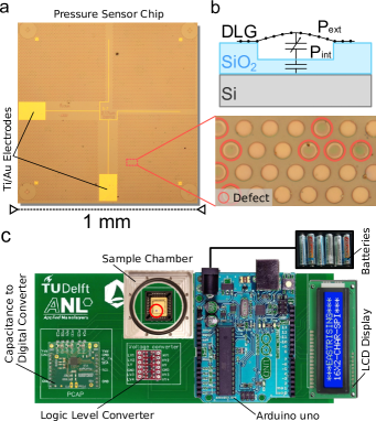
Simulations Davidovikj2017 show that to achieve the commercially competitive sensitivity, an array of around 10000 circular graphene drums is needed, each with a diameter of micron. When the drums are placed on a hexagonal grid with a pitch of 10 micron between their centers, they fit on a mm2 chip as shown in Fig. 1a. To fabricate this design, Ti/Au electrodes ( nm/ nm), for contacting the graphene top electrode, are patterned on a silicon chip with a nm SiO2 layer. Then the pattern of circular holes with a depth of nm is reactive ion etched into the SiO2. As shown in the cross-section in Fig. 1b, the cavity depth of the holes is less than the SiO2 layer thickness to prevent the graphene from touching the silicon bottom electrode, and thereby creating an electrical short-circuit between the electrodes, when one of the membranes collapses. As a last step the graphene is transferred over the cavities. We use two layers of graphene and small membrane diameter to improve the yield Cartamil2017 and the mechanical strength Barton2011 ; Lee2013 . Since the probability that pore defects align is low, the impermeability of DLG is also much higher than that of single layer graphene Bunch2008 .
To fabricate the double layer graphene (DLG), two sheets of CVD graphene are synthesized and then stacked on top of each other maintaining a pristine quality interface between the sheets. Using Polymethyl Methacrylate (PMMA) as a support layer of nm thickness, DLG is suspended over the pre-patterned circular holes in the SiO2/Si chip with Ti/Au electrodes (Fig. 1a). DLG was produced and transferred by Applied Nanolayers. From the differences in contrast between suspended, broken and collapsed drums CartamilBueno2016 ; Cartamil2017 we estimate that the dry transfer technique results in a yield of of freely suspended DLG/PMMA membranes. The red circles in the inset of Fig. 1a indicate defect drums in a damaged region of the sample and show this difference in contrast.
Sensor readout circuit board
The graphene capacitive pressure sensor responds to the difference established between the internal pressure of the reference cavity, and the external pressure of the environment, . This pressure difference results in a deflection of the atomically thin membrane and a corresponding change in capacitance Davidovikj2017 of the drum, as schematically depicted in Fig. 1b. The response of the graphene capacitive pressure sensor is high enough to be read-out by chip-scale commercial electronic components as is demonstrated using the battery-powered circuit shown in Fig. 1c. Here, the sample under test is kept in a small on-board vacuum chamber that allows local control over the external gas pressure while preventing the pressure to affect electrical read-out elements. A commercial capacitance to digital converter (AMS PCap04) is then used to record and digitize the capacitance of the sample measured at a peak-to-peak voltage V with a hundred of charge and discharge cycles of ms each. After voltage level adjustment by a logic level converter, an Arduino Uno board converts the measured capacitance into pressure using a predetermined calibration curve and displays it on an LCD screen. The circuit board is capable of measuring a change in the chip’s capacitance down to 10 aF on top of a background capacitance of a few tens of picofarads.
Effect of PMMA removal
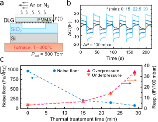
After chip fabrication and transfer, the PMMA transfer polymer still covers the DLG sheets. In a number of previous studies protective polymer layers were used to support the graphene to increase the yield, mechanical performance, hermeticity and durability of the devices, in both suspended Berger2017 ; Berger2016sheets and touch-mode operation Berger2017touch . However, the bending rigidity of the polymer layers reduces the deflection and responsivity of the membranes and sensor. To improve the sensor performance we therefore gradually remove the transfer polymer by annealing it in dry gas burningLin2011 ; burningAhn2016 ; burningHuang2014 ; burningGammelgaard2014 , as shown in Fig. 2.
The sample is put inside a furnace and left at a pressure of Torr with a constant flow of an inert dry gas (Ar or N2) at a temperature of C as schematically depicted in Fig. 2a. We found no notable difference between the use of Ar or N2 gas flow in terms of the end quality of DLG layers or PMMA removal rate. The average thickness of the transfer PMMA reduces with time at an estimated rate of nm/minute with only minor residues left on and in-between the graphene layers. The thickness reduction by thermal treatment is found to substantially improve the responsivity of the sensors. Figure 2b shows the capacitance change of a single chip to external pressure changes between and mbar with a period of 40 seconds as measured after , , and minutes of annealing. Figure 2c shows that by following the thermal anneal procedure, an increase in responsivity of almost an order of magnitude was achieved for this particular sample, while in the best case an increase in responsivity of nearly two orders of magnitude was observed after a minute continuous thermal anneal treatment. The detection noise floor also decreases substantially as a result of the process. The noise floor, , in Pa/ is defined as:
| (1) |
where is the RMS noise in the capacitance measurement, the responsivity of the sensor and Hz, the frequency at which the measurements are acquired. The decrease in as shown in Fig. 2c qualitatively follows from the equation (1) considering the measured increase in responsivity.
Results and Discussion
Sample characterization
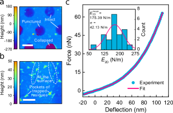
After thermal treatment for 30 minutes at C, we inspect the samples for damage. In Fig. 3a a tapping mode Atomic Force Microscopy (AFM) image of the sample is shown. Three types of drums can be distinguished visually: intact, ruptured and collapsed drums. Collapsed drums are in contact with the bottom of the cavity and probably do not significantly contribute to the response Berger2017touch because they are predominantly damaged and thus not airtight. The ruptured drums are also expected to leak fast Dolleman2015 and therefore have a negligible contribution to the static capacitance response to gradual pressure changes. Intact drums, however, show a full coverage of the cavity. These drums can hermetically seal the cavity with a constant internal pressure exploiting the extremely low permeability of graphene Bunch2008 ; Lee2019 ; SunGeim2019 , although in part of these membranes small pores can be present that are too small to be visually detected. As shown in the AFM measurements in Fig. 3b, after the anneal, a substantial number of residues are observed on and below the DLG. The residues form pockets and are also observed in the suspended regions of the device, which suggests that part of the residues is trapped in-between the graphene layers, where they cannot be easily removed residuesJain2018 .
During the fabrication, the capability of graphene to withstand high strains Lee2008 ; RuizVargas2011 ; Cui2020 facilitates damage-free transfer, while the thickness of only a few atoms favours higher membrane deflections and thus higher responsivity to pressure changes of the sensor. In order to test the elasticity and mechanical properties of the drums after thermal treatment, we use force-indention AFM to apply a point-force in the centre of a single membrane while measuring its deflection Lee2008 . The applied force, , is proportional to the stiffness of a cantilever and its deflection as . We use two cantilevers of N/m and for two separate sets of measurements in two distant places on the chip. We record a force versus membrane deflection curve at the centre of each drum, as depicted in Fig. 3c, and fit it to a model for point deflection of a circular membrane Lee2008 ; CastellanosGomez2012 :
| (2) |
where is the pre-tension, the two dimensional Young’s modulus of the layer, the Poisson’s ratio Lee2013 , the resulting deflection, the radius and a geometrical factor Lee2008 ; CastellanosGomez2012 . We use the two dimensional Young’s modulus, for the stacked DLG sheet since the thickness, , of the layer after the thermal treatment is not well defined. Such an effective quasi-2D Young’s modulus provides a more realistic estimate for the mechanical elasticity of the layer and can be directly compared to that of a pristine single layer graphene Lee2008 . In the inset of Fig. 3c, the statistics over different drums are shown that yield a mean value of N/m. This is substantially lower than reported values for both exfoliated and pristine CVD single-layer graphene Lee2008 ; Lee2013 , but comparable to other CVD graphene membranes Nicholl2015 ; RuizVargas2011 ; Li2015 ; Berger2016sheets , high-quality oxidized graphene sheets Suk2010 ; GmezNavarro2008 and other 2D materials like single-layer MoS2 CastellanosGomez2012 .
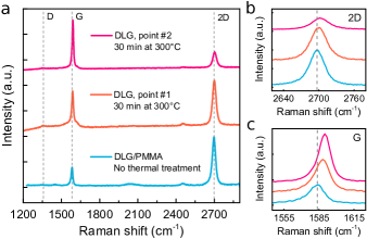
We also examined the sheets of DLG by using Raman spectroscopy, as displayed in Fig. 4. Figure 4a shows Raman spectra of DLG acquired before the removal of the PMMA layer (blue line) and after the processing at an elevated temperature (orange and magenta line). Before the thermal treatment, the Raman spectrum of DLG is reasonably homogeneous across the chip, showing a Lorenzian-shaped 2D peak of graphene and a well-defined G peak Ferrari2007 . Full width at half maximum (FWHM) of the 2D peak is around cm-1 and a high intensity ratio of 2D to G peaks resemble typical features of pristine graphene Ferrari2007 . In the case of DLG, this indicates that the two layers in the stack are well decoupled and/or have on average a twist-angle Kim2012 larger than . After processing at a high temperature, the width of the 2D peak remains the same (see Fig. 4b) while the ratio between 2D to G peaks changes drastically depending on the chosen location of the measurement on the chip (see Fig. 4a, orange and magenta lines). Also, a notable blue-shift of both 2D and G peaks is observed, as shown in Fig. 4b,c. These observations are attributed to a substantial difference in twist-angle across the DLG sheet Kim2012 as well as local changes in strain as a result of annealing of the graphene layers Ni2008 .
We also note the almost complete absence of the D peak in all Raman spectra as shown in Fig. 4a, indicating a very low amount of defects in the stacked graphene layers even after exposure to high temperatures Eckmann2012 . This result is in agreement with the outstanding high-temperature stability of graphene when encapsulated by protective layers siskins2019 ; Son2017 , and provides evidence that damage, caused by the removal of polymer from suspended graphene, is minimal burningLin2011 ; burningAhn2016 ; burningHuang2014 ; burningGammelgaard2014 .
Analysis of the sensor response
A pressure difference results in a deflection of a circular graphene membrane with radius , given by:
| (3) |
where the graphene membrane takes the shape of the section of a sphere bunch2008mechanical ; Davidovikj2017 . Since the pressure inside the reference cavity is about bar (the pressure during transfer), at bar atmospheric pressure and according to equation (3) the sensors are expected to have a linear response at small . However, at larger deflections nonlinear mechanical and capacitance effects start to result in non-linearities in the capacitance curve that can be calculated using the parallel-plate approximation Davidovikj2017 as:
| (4) |
where is the vacuum permittivity, the gap size between the membrane and bottom electrode for . The contribution of quantum capacitance of graphene is small qcPonomarenko2010 ; qcXia2009 and is neglected. The total capacitance change of the sensor can be modeled from equation (3) and (4) as:
| (5) |
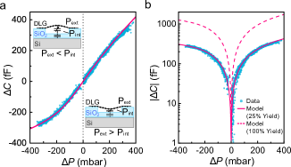
where is the number of intact, hermetic drums after both fabrication and thermal treatment. We experimentally test if equations (4) and (5) can model the graphene pressure sensor by applying both substantial negative and positive pressure differences while measuring its capacitance. Figure 5a shows the response of the same sensor that was characterized in Figs. 3 and 4.
The maximal responsivity of the sensor is achieved near ambient pressure in the linear regime, while a notable nonlinear response occurs for mbar. A number of design factors, such as the drum diameter, the number of drums and the pitch between the drums influence the sensor performance Davidovikj2017 . Importantly, the pressure dependence of can be well reproduced by the model of equation (5) using a Young’s modulus of N/m, estimated by an AFM probe for this particular sample, and a pre-tension N/m as shown by the magenta line in Fig. 5a. The model follows the measurement closely when we use a fitted value of =0.25 as shown in Fig. 5b (solid magenta line), where is the total number of drums. This indicates that the yield of intact hermetic drums is , and suggests that a large number of drums that look visually intact do not remain hermetic after polymer removal. The theoretical maximum response at a perfect yield of is also shown (dashed magenta line).
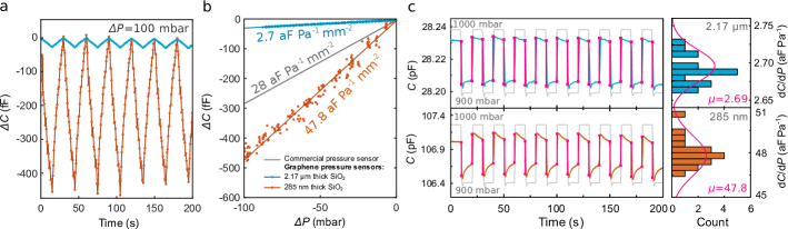
Many other factors can influence the responsivity. Since the device capacitance has a strong dependence on the distance between the plates of the pressure sensor, the cavity depth has a large influence on the performance of the sensor. In Fig. 6 we demonstrate the performance of two of the best samples with a SiO2 thickness of nm and m respectively. Both chips have circular holes with a depth of nm fabricated as described previously. Figure 6a shows the triangular wave response of both nm (orange line) and m (blue line) chips. As shown in Fig. 6b, the difference in responsivity for the two oxide thicknesses as a function of pressure can be more than an order of magnitude. Using equation (1), we calculate the noise level to be Pa/ for the nm thick SiO2 sample and Pa/ for the m one.
There is a notable scatter in the measured capacitance values as seen in Fig. 6b that is attributed to the effect of gas escaping the cavities for part of the drums, thus causing to decrease with time. It has been reported before that when graphene is suspended over a SiO2/Si cavity, it does not always form a perfect hermetic sealBunch2008 ; Lee2019 . As recently shown by Lee, et al., most of the gas permeation in graphene drums occurs along the van der Waals interface between the 2D material and the substrate Lee2019 . As a result of the contribution of this effect, an exponential decrease of with time is visible in Fig. 6c, in response to periodic pressure steps of mbar. However, if a good graphene crystallinity is preserved over large areas, the mean path that the gas needs to travel to escape the cavities becomes large, and this will increase the flow resistance of the gas channel and the permeation time constant Lee2019 ; Dolleman2016osmosis . This condition seems to be achieved across part of the sample, because no significant hysteresis was observed during the slow pressure sweeps ( minutes per sweep) in Fig. 5a and b, suggesting that of the order of 25 % of the drums maintain a constant internal pressure for , as supported by the fits in Fig. 5a and b.
Optimization of all parameters is required to achieve the best sensor performance for detecting the smallest pressure differences. In terms of responsivity our best sensor with nm of SiO2 oxide (orange dots in Fig. 6a and b), with a responsivity of aF Pa-1mm-2, already outperforms the commercially available state-of-the-art Murata SCB10H sensor with a responsivity of aF Pa-1mm-2, as shown in Fig. 6b. This is comparably larger than what was previously achieved with capacitive sensors based on atomically thin 2D membranes Davidovikj2017 ; Chen2016capac , yet competitive with a thicker suspended graphene-covered nm PMMA sheets Berger2017 with a reported responsivity of aF Pa-1mm-2 over m2 of tightly-packed hexagonal membranes. However, if yields close to and hermetic sealing of all drums is realized and the pre-tension is lowered down to N/m, the presented graphene-based 2D devices are expected to achieve a theoretical maximum responsivity of aF Pa-1mm-2 near ambient pressure. Further improvement might even be possible if the gap is reduced and the packing density of the membranes is increased.
Conclusions
Where previous studies had addressed part of the challenges related to realizing portable graphene gas pressure sensors, like the pressure sensitivity, impermeability to gasses and electrical readout, here we bridged these studies by constructing a portable, battery powered functional graphene pressure sensor that outperforms commercial devices. Using off-the-shelf systems for electronic readout and data processing, we enable capacitive readout of a mm2 array of DLG graphene pressure sensors. We realize sensor chips with a high yield of suspended membranes, resulting in a sensor responsivity of aF Pa-1mm-2. We demonstrate that thermal treatment is an effective measure for controllable thickness reduction of the support polymer layer, that leads to a significant performance improvement because the thin 2D material membranes are much more flexible than with the support polymer. It is anticipated that further design and fabrication improvements and better control over the device yield can increase the responsivity by a factor 10, thus enabling improvements in applications like indoor navigation, altitude monitoring and activity monitoring, and can enable new applications like presence detection.
Acknowledgements.
M.Š., M.L., H.S.J.v.d.Z. and P.G.S. acknowledge funding from the European Union’s Horizon 2020 research and innovation program under grant agreement number 785219.Author contributions
M.L. and D.D. designed and fabricated Si/SiO2 chips. R.v.R. and D.W. fabricated and transferred the CVD graphene stack at Applied Nanolayers B.V. M.Š. and M.L. realised a thermal removal of the polymer. T.W.d.J., J.R.R. and D.D. designed the read-out circuit board. M.Š., M.L., T.W.d.J., J.R.R., B.C.H., W.S.J.M.P. and D.D. performed capacitance measurements. T.W.d.J., J.R.R., B.C.H. and D.D. analyzed the noise level of the sensors. W.S.J.M.P. and M.Š. performed the AFM measurements. W.S.J.M.P., M.Š. and M.L. modeled a response of the sensor. D.D., H.S.J.v.d.Z. and P.G.S. conceived and supervised the project. The manuscript was jointly written by all authors with a main contribution from M.Š. All authors discussed the results and commented on the manuscript.
Conflict of interest
The authors declare that they have no conflict of interest.
References
References
- (1) Zurutuza, A. & Marinelli, C. Challenges and opportunities in graphene commercialization. Nature Nanotech. 9, 730–734 (2014).
- (2) Lee, M. et al. Sealing graphene nanodrums. Nano Lett. 19, 5313–5318 (2019).
- (3) Bunch, J. S. et al. Impermeable atomic membranes from graphene sheets. Nano Lett. 8, 2458–2462 (2008).
- (4) Sun, P. Z. et al. Limits on gas impermeability of graphene. Nature 579, 229–232 (2020).
- (5) Lee, C., Wei, X., Kysar, J. W. & Hone, J. Measurement of the elastic properties and intrinsic strength of monolayer graphene. Science 321, 385–388 (2008).
- (6) Cui, T. et al. Fatigue of graphene. Nature Mater. (2020).
- (7) Lee, G.-H. et al. High-strength chemical-vapor-deposited graphene and grain boundaries. Science 340, 1073–1076 (2013).
- (8) Chen, J.-H., Jang, C., Xiao, S., Ishigami, M. & Fuhrer, M. S. Intrinsic and extrinsic performance limits of graphene devices on SiO2. Nature Nanotech. 3, 206–209 (2008).
- (9) Chen, Y.-M. et al. Ultra-large suspended graphene as a highly elastic membrane for capacitive pressure sensors. Nanoscale 8, 3555–3564 (2016).
- (10) Berger, C., Phillips, R., Centeno, A., Zurutuza, A. & Vijayaraghavan, A. Capacitive pressure sensing with suspended graphene–polymer heterostructure membranes. Nanoscale 9, 17439–17449 (2017).
- (11) Berger, C. et al. Touch-mode capacitive pressure sensor with graphene-polymer heterostructure membrane. 2D Mater. 5, 015025 (2017).
- (12) Davidovikj, D., Scheepers, P. H., van der Zant, H. S. J. & Steeneken, P. G. Static capacitive pressure sensing using a single graphene drum. ACS Appl. Mater. Interfaces 9, 43205–43210 (2017).
- (13) Zhu, S.-E., Ghatkesar, M. K., Zhang, C. & Janssen, G. C. A. M. Graphene based piezoresistive pressure sensor. Appl. Phys. Lett. 102, 161904 (2013).
- (14) Smith, A. D. et al. Electromechanical piezoresistive sensing in suspended graphene membranes. Nano Lett. 13, 3237–3242 (2013).
- (15) Smith, A. D. et al. Piezoresistive properties of suspended graphene membranes under uniaxial and biaxial strain in nanoelectromechanical pressure sensors. ACS Nano 10, 9879–9886 (2016).
- (16) Patel, R. N., Mathew, J. P., Borah, A. & Deshmukh, M. M. Low tension graphene drums for electromechanical pressure sensing. 2D Mater. 3, 011003 (2016).
- (17) Dolleman, R. J., Davidovikj, D., Cartamil-Bueno, S. J., van der Zant, H. S. J. & Steeneken, P. G. Graphene squeeze-film pressure sensors. Nano Lett. 16, 568–571 (2015).
- (18) Romijn, J. et al. A miniaturized low power pirani pressure sensor based on suspended graphene. In 2018 IEEE 13th Annual International Conference on Nano/Micro Engineered and Molecular Systems (NEMS) (IEEE, 2018).
- (19) Rosłoń, I. E. et al. Graphene effusion-based gas sensor (2020). Preprint at https://arxiv.org/abs/2001.09509v1.
- (20) Dolleman, R. J., Cartamil-Bueno, S. J., van der Zant, H. S. J. & Steeneken, P. G. Graphene gas osmometers. 2D Mater. 4, 011002 (2016).
- (21) Cartamil-Bueno, S. J. et al. Very large scale characterization of graphene mechanical devices using a colorimetry technique. Nanoscale 9, 7559–7564 (2017).
- (22) Barton, R. A. et al. High, size-dependent quality factor in an array of graphene mechanical resonators. Nano Lett. 11, 1232–1236 (2011).
- (23) Cartamil-Bueno, S. J. et al. Colorimetry technique for scalable characterization of suspended graphene. Nano Lett. 16, 6792–6796 (2016).
- (24) Berger, C. N., Dirschka, M. & Vijayaraghavan, A. Ultra-thin graphene–polymer heterostructure membranes. Nanoscale 8, 17928–17939 (2016).
- (25) Lin, Y.-C. et al. Graphene annealing: How clean can it be? Nano Lett. 12, 414–419 (2011).
- (26) Ahn, Y., Kim, J., Ganorkar, S., Kim, Y.-H. & Kim, S.-I. Thermal annealing of graphene to remove polymer residues. Mater. Express 6, 69–76 (2016).
- (27) Huang, L.-W. et al. Characterization of the cleaning process on a transferred graphene. J. Vac. Sci. Technol. 32, 050601 (2014).
- (28) Gammelgaard, L. et al. Graphene transport properties upon exposure to PMMA processing and heat treatments. 2D Mater. 1, 035005 (2014).
- (29) Jain, A. et al. Minimizing residues and strain in 2D materials transferred from PDMS. Nanotechnology 29, 265203 (2018).
- (30) Ruiz-Vargas, C. S. et al. Softened elastic response and unzipping in chemical vapor deposition graphene membranes. Nano Lett. 11, 2259–2263 (2011).
- (31) Castellanos-Gomez, A. et al. Elastic properties of freely suspended MoS2 nanosheets. Adv. Mater. 24, 772–775 (2012).
- (32) Nicholl, R. J. et al. The effect of intrinsic crumpling on the mechanics of free-standing graphene. Nat. Commun. 6 (2015).
- (33) Li, Z. et al. Deformation of wrinkled graphene. ACS Nano 9, 3917–3925 (2015).
- (34) Suk, J. W., Piner, R. D., An, J. & Ruoff, R. S. Mechanical properties of monolayer graphene oxide. ACS Nano 4, 6557–6564 (2010).
- (35) Gómez-Navarro, C., Burghard, M. & Kern, K. Elastic properties of chemically derived single graphene sheets. Nano Lett. 8, 2045–2049 (2008).
- (36) Ferrari, A. C. Raman spectroscopy of graphene and graphite: Disorder, electron–phonon coupling, doping and nonadiabatic effects. Solid State Commun. 143, 47–57 (2007).
- (37) Kim, K. et al. Raman spectroscopy study of rotated double-layer graphene: Misorientation-angle dependence of electronic structure. Phys. Rev. Lett. 108 (2012).
- (38) Ni, Z. H. et al. Tunable stress and controlled thickness modification in graphene by annealing. ACS Nano 2, 1033–1039 (2008).
- (39) Eckmann, A. et al. Probing the nature of defects in graphene by raman spectroscopy. Nano Lett. 12, 3925–3930 (2012).
- (40) Šiškins, M. et al. High-temperature electronic devices enabled by hBN-encapsulated graphene. Appl. Phys. Lett. 114, 123104 (2019).
- (41) Son, S.-K. et al. Graphene hot-electron light bulb: incandescence from hBN-encapsulated graphene in air. 2D Mater. 5, 011006 (2017).
- (42) Bunch, J. S. Mechanical and electrical properties of graphene sheets (Cornell University Ithaca, NY, 2008).
- (43) Ponomarenko, L. A. et al. Density of states and zero landau level probed through capacitance of graphene. Phys. Rev. Lett. 105 (2010).
- (44) Xia, J., Chen, F., Li, J. & Tao, N. Measurement of the quantum capacitance of graphene. Nature Nanotech. 4, 505–509 (2009).