Charge-based Modeling of Ultra Narrow
Cylindrical Nanowire FETs
Abstract
This brief proposes an analytical approach to model the dc electrical behavior of extremely narrow cylindrical junctionless nanowire field-effect transistor (JL-NW-FET). The model includes explicit expressions, taking into account the first order perturbation theory for calculating eigenstates and corresponding wave functions obtained by the Schrödinger equation in the cylindrical coordinate. Assessment of the proposed model with technology computer-aided design (TCAD) simulations and measurement results confirms its validity for all regions of operation. This represents an essential step toward the analysis of circuits mainly biosensors based on junctionless nanowire transistors.
Cylindrical FETs, Junctionless FETs, Nanowire FETs, Quantum Confinement, first order perturbation.
1 Introduction
Junctionless (JL) Silicon nanowire FETs with heavily doped channel, typically in the range of cm-3 to cm-3, have been the subject of intensive research both in the fields of fabrication process and modeling. Due to its extremely interesting morphological and functional bio-compatible for sensing applications [1, 2], silicon nanowire has been broadly used for the label-free detection in chemical and biological experiments[3, 4]. Given the advantage of using junctionless silicon nanowires in a wide range of applications, especially for sensing applications, several compact models have been proposed so far [5, 6]. Relying on the Poisson-Boltzmann equations, the charge-based models were developed to model junctionless double-gate and nanowire FETs in [7, 8, 9]. However, those models overestimate the drain to source current and free carrier charge density for the channel thicknesses less than nm due to the charge quantization into discrete sub-bands, which was not taken into account in classical models. To accurately capture the quantization effects, we recently proposed a charge-based model, including quantum confinement for ultra-thin junctionless double-gate FETs and GAA Junctionless nanowire [10] and [11]. The proposed approach relies on the Schrödinger equation with the order perturbation theory and Fermi-Dirac statistics. In this context, extending the proposed approach, we derive an explicit model for extremely narrow cylindrical junctionless nanowire FET which has easier fabrication and higher surface to volume ratio compared to rectangular cross-section nanowire, which are important features for nano-scaled sensor structures. cylindrical device also exhibit uniform distribution of potential and electric field around its surface without electric field crowding near the corners, making this structure a candidate for sensing application. Thus, taking into account the stated advantages, we concentrate on the derivation of a simple analytical model for extremely narrow cylindrical junctionless nanowire FET for biosensing applications.
2 Electrostatics in Ultrathin Junctionless Cylindrical Nanowire FETs
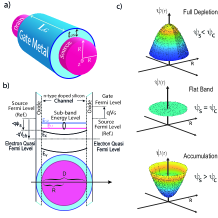
We consider an n-type junctionless cylindrical nanowire with diameter and radius . Fig. 1(a) shows a 3D schematic view of a cylindrical junctionless nanowire. When the gate to channel voltage is below the flat-band potential, we may assume full depletion approximation and neglect free carrier charge density assuming parabolic approximation for the potential profile across the channel as a solution of the Poisson equation. Hence, the potential distribution across the channel can be expressed simply as:
| (1) |
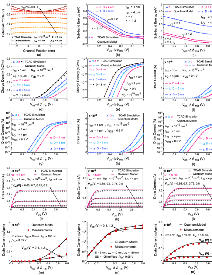
Where and are the electrostatic potentials at the center and surface of the cylindrical channel. On the contrary, by increasing the gate voltage above the threshold, the density of electrons in the few lowest subbands increases rapidly according to Fermi-Dirac statistics in a system with 2D confinement [12]. Fig. 2(a) represents the potential profile across the channel, which compares TCAD simulation results with the proposed model for nm, from depletion to accumulation mode. Physical parameters for cylindrical JL nanowire FET used in the TCAD simulations and model are listed in Table 1. This confirms the validity of parabolic approximation for both depletion and accumulation modes, by properly including the impact of carrier charges in () term. As seen, the second derivative of the potential profile versus , which is proportional to the total charge density, becomes positive/negative when the device enters into accumulation/depletion modes of operation. While the channel is neutral and , the values of surface and center potentials become equal, i.e. flat-band condition (see Fig. 1(b)). The electric field at the channel-oxide interface, , can be obtained using (1) and is linked to the overall space charge density. Imposing the boundary conditions at the perimeter of the channel, the electric field can be given as a function of center and surface potentials by
| (2) |
where . For any channel cross section with radius R, one may write the Gauss law in circular coordinate:
| (3) |
is the gate dielectric capacitance per unit area given by
| (4) |
Combining (2) and (3) gives a relationship between surface and center potentials for a given gate voltage:
| (5) |
On the other hand, the total charge density per unit length is the sum of the mobile charge density, , and fixed-charge density, , given by
| (6) |
Here mobile charge calculate by assuming 2D confinement of electron in the channel for ( nm) and relying on Fermi Dirac integral in order of and 1D density of state [13, 14] we propose to estimate the mobile charge density, , by
| (7) |
where is the difference between the first sub-band eigenstate energy level and electron quasi-Fermi level . As shown in Fig. 1(c) electron quasi-Fermi level varies from at the source to at the drain terminal. Moreover, represents 1D density of state. we further assume that only two degenerate valleys () of the first sub-band () contribute to .
3 Eigenstate Energy Levels in Cylindrical Coordinate and Electron Charge Density
As stated in [10] Solving the Schrödinger equation, for an ideal circular infinite quantum well around the channel at Si-SiO2 interface, eigenstate energy levels and electron wave-functions in discrete sub-bands are given by
| (8) |
| (9) |
| Parameter | Symbol | Value |
|---|---|---|
| Channel Doping | cm-3 | |
| Channel Diameter | nm | |
| Oxide Thickness | nm | |
| Channel Width | m | |
| Permittivity in Vacuum | F/m | |
| Silicon Permittivity | ||
| Silicon Oxide Permittivity | ||
| longitudinal Effective mass | ||
| Transverse Effective mass | ||
| Silicon Band Gap | eV | |
| Gate Work Function | eV | |
| Conduction Band effective DoS | cm-3 | |
| Valence Band Effective DoS | cm-3 | |
| Silicon Intrinsic Carrier Density | cm-3 | |
| Temperature | K | |
| Thermal Voltage | V | |
| First zero of | ||
| Second zero of |
Here, and are Bessel functions of the first kind and is zero of . The terms of and are used to calculate the first and the second eigenstate energy levels in the absence of electrostatic potential perturbation respectively. The term of corresponds to the electron effective mass inside the channel. In this study, the effective masses are taken as for the first valley and = for the second valley in a -oriented Si channel [15]. The first order perturbation theory is used to calculate the impact of electrostatic potential on sub-band energies:
| (10) |
Substituting from (1) and from (9) into (10) leads to an analytical expression for the first order perturbation energy in the cylindrical coordinate:
| (11) |
Total sub-band energy which results from geometrical and electrical confinements is the sum of energies obtained in (8) and (11):
| (12) |
Fig. 2(b) and (c) demonstrate for two first sub-bands and degenerate valleys measured from electron energy at the channel surface as a reference. Although simulation results show a good agreement compare to model for both sub-bands and degenerate valleys but only the first sub-band considered in model calculations, which reduce model computation. The occupation percent of electrical charge in the two lowest sub-bands indicates that the error in the charge density is less than for nm channel diameter when we neglect contributions of higher subbands () in charge density calculations. However, to calculate the charge density more preciously, additional sub-band should be included. Fig. 2(d) and (e) show the mobile charge density concerning the effective gate voltage for different channel diameters, i.e., nm calculated from the proposed model and validated by TCAD simulations results. In what follows, we discuss drain-current derivation in which we use (7) and (12) to calculate channel charge density.
4 Drain Current Derivation in Cylindrical JL-NW-FET
As done in [11], relying on the drift-diffusion transportation mechanism, the total drain current for both depletion and accumulation regions can be obtained by
| (13) |
Here, the term is the free carrier mobility, and define as the differences between the first sub-band and quasi-Fermi levels at the source and drain sides of the channel. Differentiating with respect to the we get:
| (14) |
Using (5), can be expressed as
| (15) |
Next, using (11) and (5) and applying the chain rule , we obtain:
| (16) |
Here, is a key parameter which depends on the channel diameter and gate oxide thickness. Now we can write based on (14), (15) and (16) as follows:
| (17) |
where . Substituting (17) into (13) leads to:
| (18) |
Replacing from (7) in (18), and after integrating, we obtain an analytical expression for the drain current:
| (19) |
5 Results and Discussion
Fig. 2(f) and (h) show the drain current versus the effective gate voltage at low () and high () drain potentials for linear and saturation modes of operation. Fig. 2(j), (k), and (l) show the drain current with respect to for nm respectively for several above the flat-band condition. Additionally, fig. 2(m), (n), and (o) show the drain current comparison of model results and experimental data for cylindrical junctionless nanowire with nm, nm and nm [16]. To compare our model which is based on long channel approximation with experimental data with nm channel length, we introduced a correction factor in such a way that in (7) will now be replaced by to recover the mismatch in the subthreshold region for drain current (see Fig.2 (n)). It worth highlighting that for long channel length devices, the suggested model gives an accurate prediction of the carrier charge density without any correction factor.
A self-consistent coupled Schrödinger-Poisson model has been used in TCAD simulations for mobile charge density and band state energy derivation. For the current calculation, we used the Bohm Quantum Potential model in our simulation. TCAD assures that there is a close agreement between Bohm Quantum Potential and the results of Schrödinger-Poisson model calculations for any given class of device. The result predicted by the model shows excellent agreement with TCAD simulations, in both linear and saturation regions. TCAD simulation results verify that the proposed model works well for both depletion and accumulation regions for the device with an extremely narrow channel size ( nm).
Before concluding, we would like to say few words about the limitations of this model. As simulation results indicated, the model demonstrates excellent accuracy for nm. However, as shown in Fig.2(d), for channel diameter larger than nm the model predicted charge density deviates from simulation results. Indeed, by increasing channel diameter, the potential distribution in the channel does not follow the parabolic approximation anymore. As a result, first-order perturbation theory (11) can not correctly predict discrete sub-bands’ energy and higher order interactions should be taken into account. Moreover, the energy distance between sub-bands decreases and therefore the charge in several subbands participate in the conduction process. Another important consideration is variability due to random fluctuations in ultra-thin devices with high doping concentration. A capillary channel with high doping concentration caused a random position of a few impurity atoms in the channel, which has a critical impact on model validity due to device to device variations. This issue is critical for VLSI applications, however as discussed in [11], it is not a major concern as long as we focused on biosensing applications.
6 Conclusion
In this paper, we developed a simple analytical model for 2D electrostatic potential distribution and charge density of extremely narrow cylindrical nanowire FETs. Takes in to account cylindrical coordination and first-order correction for the confined energies analytical solution developed for discrete energy sub bands. Moreover, by using drift-diffusion method we derived simple analytical expression for drain current. The validity of the model verified by TCAD simulations and also experimental data for a device with channel diameter in the range of to nm. Results evaluation confirms that the proposed model can capture precisely the dc behavior of such device for all regions of operation. In addition, this approach might also be used to derive trans-capacitance model for ac analysis with cylindrical junctionless nanowire devices[17, 18].
References
- [1] R. R. Singh, A. Singh, A. Gautam, and V. Priye, “Vertical silicon nanowire-based optical waveguide for dna hybridization biosensor,” in Quantum Sensing and Nano Electronics and Photonics XVI, vol. 10926. International Society for Optics and Photonics, 2019, p. 109262M.
- [2] R. Smith, W. Duan, J. Quarterman, A. Morris, C. Collie, M. Black, F. Toor, and A. K. Salem, “Surface modifying doped silicon nanowire based solar cells for applications in biosensing,” Advanced Materials Technologies, vol. 4, no. 2, p. 1800349, 2019.
- [3] Jean-Pierre Colinge, Chi-Woo Lee, Aryan Afzalian, Nima Dehdashti Akhavan, Ran Yan, Isabelle Ferain, Pedram Razavi, Brendan O’Neill, Alan Blake, Mary White, Anne-Marie Kelleher, Brendan McCarthy, and Richard Murphy, “Nanowire Transistors Without Junctions,” Nature Nanotechnology, vol. 5, pp. 225–229, February 2010.
- [4] J.-H. Lee, E.-J. Chae, S.-j. Park, and J.-W. Choi, “Label-free detection of -aminobutyric acid based on silicon nanowire biosensor,” Nano convergence, vol. 6, no. 1, p. 13, 2019.
- [5] T. Numata, S. Uno, J. Hattori, G. Mil’nikov, Y. Kamakura, N. Mori, and K. Nakazato, “A Self-Consistent Compact Model of Ballistic Nanowire MOSFET With Rectangular Cross Section,” IEEE Transactions on Electron Devices, vol. 60, no. 2, pp. 856–862, Feb 2013.
- [6] N. Makris, F. Jazaeri, J. Sallese, and M. Bucher, “Charge-based modeling of long-channel symmetric double-gate junction fets—part ii: Total charges and transcapacitances,” IEEE Transactions on Electron Devices, vol. 65, no. 7, pp. 2751–2756, July 2018.
- [7] J. Sallese, N. Chevillon, C. Lallement, B. Iniguez, and F. Pregaldiny, “Charge-based Modeling of Junctionless Double-Gate Field-Effect Transistors,” IEEE Transactions on Electron Devices, vol. 58, no. 8, pp. 2628–2637, Aug 2011.
- [8] F. Jazaeri and J.-M. Sallese, Modeling Nanowire and Double-Gate Junctionless Field-Effect Transistors. Cambridge University Press, 2018.
- [9] F. Jazaeri, L. Barbut, and J. Sallese, “Generalized charge-based model of double-gate junctionless fets, including inversion,” IEEE Transactions on Electron Devices, vol. 61, no. 10, pp. 3553–3557, Oct 2014.
- [10] M. Shalchian, F. Jazaeri, and J. Sallese, “Charge-Based Model for Ultrathin Junctionless DG FETs, Including Quantum Confinement,” IEEE Transactions on Electron Devices, vol. 65, no. 9, pp. 4009–4014, Sep. 2018.
- [11] D. Shafizade, M. Shalchian, and F. Jazaeri, “Ultra-thin junctionless nanowire fet model, including 2d quantum confinements,” IEEE Transactions on Electron Devices, vol. 66, pp. 4101 – 4106, 2019. [Online]. Available: https://ieeexplore.ieee.org/document/8790978
- [12] T. Numata, S. Uno, K. Nakazato, Y. Kamakura, and N. Mori, “Analytical compact model of ballistic cylindrical nanowire metal–oxide–semiconductor field-effect transistor,” Japanese Journal of Applied Physics, vol. 49, no. 4, p. 04DN05, 2010.
- [13] J.-M. Sallese, F. Jazaeri, L. Barbut, N. Chevillon, and C. Lallement, “A common core model for junctionless nanowires and symmetric double-gate fets,” IEEE Transactions on Electron Devices, vol. 60, pp. 4277–4280, 2013. [Online]. Available: https://ieeexplore.ieee.org/document/6655966
- [14] E. G. Marin, F. G. Ruiz, I. M. Tienda-Luna, A. Godoy, P. Sánchez-Moreno, and F. Gámiz, “Analytic potential and charge model for iii-v surrounding gate metal-oxide-semiconductor field-effect transistors,” Journal of Applied Physics, vol. 112, no. 8, p. 084512, 2012. [Online]. Available: https://doi.org/10.1063/1.4759275
- [15] J. P. Duarte, M. Kim, S. Choi, and Y. Choi, “A compact model of quantum electron density at the subthreshold region for double-gate junctionless transistors,” IEEE Transactions on Electron Devices, vol. 59, no. 4, pp. 1008–1012, April 2012.
- [16] N. Singh, A. Agarwal, L. K. Bera, T. Y. Liow, R. Yang, S. C. Rustagi, C. H. Tung, R. Kumar, G. Q. Lo, N. Balasubramanian, and D. . Kwong, “High-performance fully depleted silicon nanowire (diameter /spl les/ 5 nm) gate-all-around cmos devices,” IEEE Electron Device Letters, vol. 27, no. 5, pp. 383–386, May 2006.
- [17] F. Jazaeri, L. Barbut, and J.-M. Sallese, “Trans-capacitance modeling in junctionless gate-all-around nanowire fets,” Solid-State Electronics, vol. 96, pp. 34 – 37, 2014. [Online]. Available: http://www.sciencedirect.com/science/article/pii/S0038110114000707
- [18] F. Jazaeri, L. Barbut, and J. Sallese, “Trans-capacitance modeling in junctionless symmetric double-gate mosfets,” IEEE Transactions on Electron Devices, vol. 60, no. 12, pp. 4034–4040, Dec 2013.