Potassium-intercalated bulk HfS2 and HfSe2: Phase stability, structure, and electronic structure
Abstract
We have studied potassium-intercalated bulk HfS2 and HfSe2 by combining transmission electron energy loss spectroscopy, angle-resolved photoemission spectroscopy and density functional theory calculations. The results reveal insights into (1) the intercalation process itself, (2) its effect on the crystal structures, (3) the induced semiconductor-to-metal transitions, and (4) the accompanying appearance of charge carrier plasmons and their dispersions.
Calculations of the formation energies and the evolution of the energies of the charge carrier plasmons as a function of the potassium content show that certain, low potassium concentrations are thermodynamically unstable. This leads to the coexistence of undoped and doped domains if the provided amount of the alkali metal is insufficient to saturate the whole crystal with the minimum thermodynamically stable potassium stoichiometry. Beyond this threshold concentration the domains disappear, while the alkali metal and charge carrier concentrations increase continuously upon further addition of potassium.
At low intercalation levels, electron diffraction patterns indicate a significant degree of disorder in the crystal structure. The initial order in the out-of-plane direction is restored at high while the crystal layer thicknesses expand by . Calculations suggest that this expansion reaches its maximum at doping levels of before it reverses slightly for higher concentrations. Superstructures emerge parallel to the planes which we attribute to the distribution of the alkali metal rather than structural changes of the host materials. The in-plane lattice parameters change by not more than .
The introduction of potassium causes the formation of charge carrier plasmons whose nature we confirmed by calculating the loss functions and their intraband and interband contributions. The observation of this semiconductor-to-metal transition is supported by calculations of the density of states (DOS) and band structures as well as angle-resolved photoemission spectroscopy.
The calculated DOS hint at the presence of an almost ideal two-dimensional electron gas at the Fermi level for .
The plasmons exhibit quadratic momentum dispersions which is in agreement with the behavior expected for an ideal electron gas.
pacs:
79.20.UV, 71.35.-y,73.21.AcI INTRODUCTION
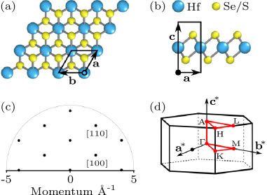
Hafnium disulfide and hafnium diselenide are semiconducting transition metal dichalcogenides (TMDCs). Their crystals are formed by slabs (molecular layers) linked by relatively weak Van-der-Waals forces. Each slab consists of an atomic hafnium layer sandwiched between two atomic sulfur/selenium layers [Fig. 1 (b)]. The compounds typically assume the -polytype in which a unit cell comprises only one molecular layer and six S/Se atoms are coordinated octahedrally around a hafnium atom (space group: , ) resulting in a triangular arrangement of the atoms in the planes [Fig. 1 (a)] McTaggart and Wadsley (1958); Greenaway and Nitsche (1965); Conroy and Park (1968); Bayliss and Liang (1982). The weak interlayer bonding gives rise to quasi-two dimensional properties. This strong anisotropy, band gaps of and predicted electron mobilities as well as sheet current densities Fiori et al. (2014) that are significantly higher than in many other TMDCs make the two compounds interesting candidates for electronic devices. So far, transistors Mleczko et al. (2017); Kanazawa et al. (2016), field-effect transistors Kang et al. (2015, 2017); Xu et al. (2016); Chae et al. (2016); Chang (2015); Fu et al. (2017); Nie et al. (2017); Kaur et al. (2018); Gong et al. (2013), phototransistors Xu et al. (2015); De Sanctis et al. (2018); Yin et al. (2016) and photodetectors Zheng et al. (2016); Yan et al. (2017); Wang et al. (2018); Mattinen et al. (2019) have been realized in experiments. The materials are also considered for photovoltaic Gaiser et al. (2004) and photocatalytic Singh et al. (2016) applications.
Although the available body of research is somewhat smaller compared to other TMDCs such as MoS2, the pristine materials have been investigated with a wide range of experimental techniques such as various optical methods Yan et al. (2017); Greenaway and Nitsche (1965); Terashima and Imai (1987); Mattheiss (1973); Beal et al. (1972); Lucovsky et al. (1973); Hughes and Liang (1977); Bayliss and Liang (1982); Gaiser et al. (2004); Fong et al. (1976); Borghesi et al. (1984a, b, 1986); Fu et al. (2017); Yan et al. (2017), photoemission Shepherd and Williams (1974); Jakovidis et al. (1987); Kreis et al. (2000); Traving et al. (2001); Aretouli et al. (2015); Zheng et al. (2016); Fu et al. (2017), x-ray diffraction Hodul and Stacy (1984); Wang et al. (2018), and Raman spectroscopy Iwasaki et al. (1982); Kanazawa et al. (2016); Xu et al. (2015); Chae et al. (2016); Zheng et al. (2016); Ibáñez et al. (2018); Fu et al. (2017); Nie et al. (2017); Yan et al. (2017); Kaur et al. (2018); Najmaei et al. (2018); Mattinen et al. (2019); Roubi and Carlone (1988); Kang et al. (2015); Yin et al. (2016); Kang et al. (2017); Cruz et al. (2018); Cingolani et al. (1988); Wang et al. (2018). But also resistivity Hodul and Stacy (1984); Zheng et al. (1989); McTaggart (1958); Radhakrishnan and Mohanan Pilla (2008), conductivity Conroy and Park (1968); Najmaei et al. (2018) Hall coefficient,Zheng et al. (1989), magnetic susceptibility Conroy and Park (1968), scanning transmission electron microscopy Aretouli et al. (2015), and electron energy-loss Bell and Liang (1976); Habenicht et al. (2018) experiments were performed. The investigations were supported by numerous theoretical approaches Murray et al. (1972); Mattheiss (1973); Fong et al. (1976); Bullett (1978); Traving et al. (2001); Zhang et al. (2014); Lebègue et al. (2013); Eknapakul et al. (2018); Chae et al. (2016); Nie et al. (2017); Reshak and Auluck (2005); Zhao et al. (2017); Jaiswal et al. (2018); Najmaei et al. (2018).
The weak Van-der-Waals interactions among the molecular layers allow introducing intercalants into the gaps between the slabs. This could alter the properties of the compounds significantly by affecting the atomic arrangements, band structures and band fillings, depending on the intercalants’ sizes and electro-negativities. This variability of characteristics makes intercalated TMDCs interesting for new applications and as research objects to obtain a better understanding of fundamental physical phenomena. Besides transition metals Yacobi et al. (1979); Iwasaki et al. (1983); Pleshchev et al. (2011), which have been intercalated into both materials, alkali metals have been used as electron donors for HfSe2 Dines (1975); Whittingham and Gamble Jr (1975). Lithium Õnuki et al. (1982); Beal and Nulsen (1981) and sodium Mleczko et al. (2017); Eknapakul et al. (2018) doping leads to a transition from semiconducting to metallic behavior. In the pristine materials, the valence states are mainly comprised of S/Se -orbitals which are almost filled due to a transfer of electrons from the hafnium atoms Camassel et al. (1977).
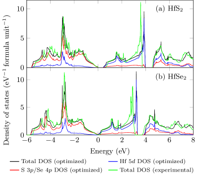
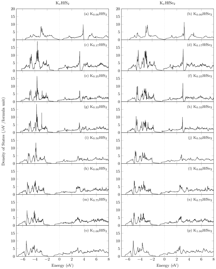
The conduction bands are formed largely by empty Hf -states McTaggart (1958); Camassel et al. (1977) that are split into and orbitals Gong et al. (2013). The nature of the orbitals comprising the valence and conduction bands is reflected in the calculated density of states (DOS) in Fig. 2. Intercalated alkali-metal atoms donate electrons to the lowest conduction bands of the host materials leading to the mentioned semiconductor-to-metal transition.
This transition made the two hafnium compounds attractive for a study using transmission electron energy-loss spectroscopy (EELS) supported by angle-resolved photoemission spectroscopy (ARPES). In particular, EELS permits the momentum dependent measurement of plasmons, the collective oscillations of charge carriers, typically associated with the free electron gas in metals Nozières and Pines (1959); Raether (2006). We combined the two experimental methods with density-functional theory (DFT) calculations to shed light on the effects of doping on crystal structures, the semiconductor-to-metal transitions, the charge carrier plasmons, and the dimensionality of the conduction bands of the title compounds. This research is a continuation of our previous efforts to investigate the effects of alkali-metal doping on TMDCs via EELS for KxTaS2, NaxTaSe2, KxNbSe2, NaxNbSe2 Müller et al. (2016), KxTaSe2 König et al. (2012, 2013), K2WSe2 Ahmad et al. (2017) and KxMoS2 Habenicht et al. .
II EXPERIMENT
II.1 EELS Experiments
EELS is a bulk sensitive scattering technique. The spectra are proportional to the loss function Sturm (1993). In this equation, is the energy 111Please note that the terms energy and frequency are used synonymously in the work (). and momentum q dependent dielectric function. For our experiments, we purchased bulk single crystals of hafnium disulfide and hafnium diselenide from HQ Graphene and cleaved them ex situ into thin films of approximately thickness using adhesive tape. Mounted on platinum transmission electron microscopy grids, the samples were measured in a purpose-built transmission electron energy-loss spectrometer operating with a primary electron energy of and equipped with a helium flow cryostat (see Refs. Fink, 1989; Roth et al., 2014 for more detailed descriptions of the instrument).
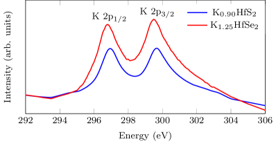
The intercalation was performed by thermally evaporating potassium from SAES alkali metal dispensers onto the samples in an ultrahigh vacuum chamber (base pressure below ) directly attached to the instrument. The films were placed in the potassium vapor for time periods ranging from 15 to and subsequently annealed for approximately at between each EELS measurement to attain a series of increasing doping levels in the same samples. The highest achieved potassium concentrations were 0.90 and 1.25 for HfS2 and HfSe2, respectively (see Sec. II.2 for a description of the method used to calculate the doping levels) because additional intercalation attempts did not change the diffraction patterns nor the loss spectra.
For an energy range between 0.2 and , the EELS spectra for the pristine and intercalated materials were acquired for a momentum transfer of in the and directions of the Brillouin zone (see Fig. 1 (d) for a picture of the Brillouin zone and its high symmetry points). The same was done for spectra up to for various |q| between 0.075 and . We also obtained electron diffraction patterns along those orientations in the momentum region at zero energy transfer (). For selected doping levels, sets of such diffraction patterns were measured consecutively in steps across at least one half of the Brillouin zone and subsequently combined to form in-plane diffraction maps. In all those cases, the energy and momentum resolutions were and . Moreover, core level spectra of sulfur/selenium and potassium were obtained with resolutions of and .
Long-time EELS measurements did not reveal noticeable beam damage in the crystals. Decomposition effects such as the formation of salts (e.g. K2S or K2Se), which were reported for MoS2 highly doped with potassium Somoano et al. (1973); Zhang et al. (2015), sodium Wang et al. (2014) or lithium Cheng et al. (2014); Huang et al. (2018), were not observed in this investigation. Such a chemical reaction would cause a splitting of the two K core level peaks in the EELS spectra because of the concurrent presence of potassium in the salt and potassium in the Van-der-Waals gaps. The K spectra in Fig. 3 do not show such a behavior even at the highest achieved alkali metal concentrations.
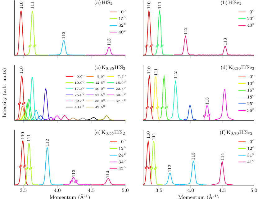
The -planes of the two materials align with the sample surfaces and are initially positioned perpendicular to the electron beam. In this configuration, the crystal planes are parallel to the momentum transfer of the scattered electrons which lies in a plane perpendicular to the beam. The instrument allows to rotate the sample surfaces up to with respect to the momentum transfer plane. We will refer to this angle as polar angle which is offset from the angle of incidence. The spectrometer does not permit diffraction measurements directly in the -direction. However, information for this direction can be acquired by adjusting the polar angle until the reciprocal lattice points of an adjacent crystal lattice layer are aligned with the momentum transfer plane such that the diffraction peak associated with the neighboring plane can be detected. The momentum positions of two Bragg peaks that are equivalent in the planes but not in the out-of-plane direction (e.g. [110] and [111]) can than be related via the Pythagorean theorem to calculate the separation of the planes in momentum space and the layer thickness in real space. This approach may be repeated for successive planes (e.g. [110], [111], [112],…) up to the maximum polar angle of .
In an effort to deduce the unscreened plasmon frequencies from the spectra of the intercalated samples, Kramers-Kronig analyses were carried out. The resulting optical conductivity functions were fitted according to the Drude-Lorentz model. This classical approach models the dielectric function as a function of the frequency of a series of oscillators representing the excitation of the involved free (Drude term) and bound (Lorentz term) charges Li (2017); Hecht (2017):
| (1) |
Here, is the index number of each oscillator in the sum, refers to the resonant frequency of the -th oscillator, and represent the frequency widths (damping factors) of the Drude and -th Lorentz oscillator, respectively. Further, is the background dielectric constant combining the effects of oscillators not included in the sum.
The oscillator strengths are expressed by the plasmon frequencies ():
| (2a) | |||
| (2b) | |||
Here, is the permittivity of free space, the elementary electron charge, () the electron density and () the effective electron mass related to the Drude oscillator (the -th Lorentz oscillator). As defined in Equ. 2a, represents the unscreened plasmon frequency of the free electrons. It differs from the screened plasmon frequency reflected in electron energy-loss spectra due to damping by single particle excitations in the surrounding host material.
II.2 Calculation of Intercalation Levels in EELS Measurements
Due to the setup of the experiments, it was not possible to measure the potassium concentration in the crystals in a direct way. As an alternative, the charge carrier plasmon peak position (see Sec. IV.2) was extracted from the EELS response associated with the intercalation step that produced the most pronounced plasmon peak in an intercalation series. The peak position was determined after eliminating the effects of the quasielastic line by fitting the latter with a Gaussian function and the plasmon feature with the loss function of a Drude oscillator (see Ref. Schuster et al., 2009 for details). The peak energies found in this way were matched with the interpolated plasmon peak energies from the DFT loss spectra (see Sec. IV.2) for compounds with various simulated potassium stoichiometries. This comparison of experimental and simulated plasmon peak energies allowed the assignment of the interpolated simulated doping levels to the experimental intercalation step. The specific spectra to which the described procedures were applied turned out to be the ones with doping levels of for HfS2 and for HfSe2. All other doping levels were determined by calculating the areas under the K core level peaks for each intercalation step. The integration was performed after deducting a linear background between 293.5 and from the spectra. The fractional changes of each area relative to the area for which the doping levels were determined from the plasmon peak positions were multiplied with the concentrations stated above ( and ) to find the potassium concentrations for the other intercalation steps.
II.3 Photoemission Measurements
The photoemission measurements were performed at room temperature in an instrument with a base pressure of equipped with a Scienta R4000 electron analyzer, a helium discharge lamp with a photon energy of (He II) and an Al x-ray source with energy of . The crystals were attached to copper sample holders with electrically conductive EPO-TEK H27D epoxy and cleaved in situ. The potassium deposition on the samples was achieved by thermal evaporation from SAES alkali metal dispensers. The Fermi energy Ef was determined by fitting the Fermi edge of a gold sample measured under the same conditions. The alkali metal concentrations in the samples were derived from the fractions of the cross section adjusted Hf and K XPS core level peak areas.
The experimental setup does not allow an in situ transfer of the samples between the EELS and the ARPES spectrometers. Consequently, it was not possible to apply both methods to the same specimens and intercalations had to be performed in each instrument separately.
III COMPUTATIONAL DETAILS
To support the interpretation of the experimental results, we carried out density function theory calculations using the 18.00-52 version222https://www.fplo.de/ of the full-potential local-orbital code (FPLO) Koepernik and Eschrig (1999); Richter et al. (2008). The Perdew-Wang-92 exchange-correlation-functional Perdew and Wang (1992) of the local density approximation (LDA) was employed. The linear tetrahedron method with Blöchl corrections was applied for -space integrations. We checked the importance of the spin-orbit interaction for the case of HfSe2. A comparison of the DOS of HfSe2 with and without spin-orbit interaction showed differences of up to in the band edges but an almost perfect overall agreement in the whole relevant energy range between and (not shown). Hence, we decided to perform all further calculations only in the scalar relativistic mode.
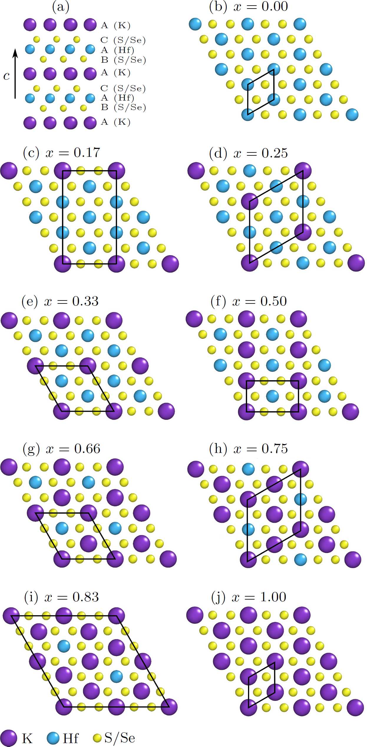
Calculations were carried out for undoped bulk compounds and for certain structural configurations of K-doped bulk materials. The pristine crystals consist of planes in the sequence: A (Hf) - B (S/Se) - C (S/Se) - A(Hf). The intercalated bulk structures for potassium concentrations up to were constructed by placing K-atoms into the Van-der-Waals gaps such that they occupy the A positions in the sequence: A (Hf) - B (S/Se) - A(K) - C (S/Se) - A(Hf) (see Fig. 14 (a) in Appendix VI). Supercells extending in the -plane were set up containing the appropriate number of potassium atoms to achieve the desired stoichiometries (see Fig. 14 (b) - (j) in Appendix VI).
For all considered structures, an iterative process was used to optimize the lattice parameters. In each iteration step, one of the lattice constant was changed and the atomic positions were optimized by minimizing the total energy within the limitations of the applied space groups and an accuracy of on each atom.
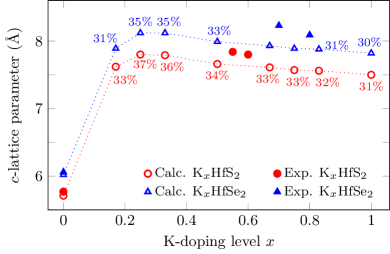
In addition, we also used experimental lattice constants for the undoped materials. In those cases, only the internal parameters were relaxed. The calculated lattice parameters underestimated the experimental values by or less which is typical for LDA calculations Jiang (2011).
We should note that, materials with important contributions of Van-der-Waals bonding require the consideration of the related dispersion forces for accurate structure optimization. Here, we neglect these contributions and instead rely on error compensation with the known LDA overbinding. The obtained realistic lattice parameters (Fig. 4) provide an a posteriori justification for our approach.
All used space groups, -meshes, optimized atomic coordinates as well as experimental and optimized lattice parameters are listed in Tables LABEL:tab:HfS2_CalcDetails and LABEL:tab:HfSe2_CalcDetails of Appendix VI. The band structures, densities of states, formation energies, and optical properties, in particular the loss functions and their interband and intraband contributions, were calculated for all structures described in those tables. The intraband contributions correspond to the Drude terms in Equ. 2a modeling the behavior of the free electrons in a metal and, therefore, reflect charge carrier plasmons. They are collective oscillations of all conduction electrons. Frequency widths of and were applied to the Drude contributions (Equ. 1) of HfS2 and HfSe2, respectively, to match the calculated plasmon peak widths to the experimental spectra.
In order to test convergence, calculations with finer -meshes () were performed for the pristine bulk materials with optimized lattice constants but did not yield any relevant improvements in the DOS.
ARPES measurements are surface sensitive since the contributions of the photoelectrons to the intensity of the spectra decrease with the distance of the emitting atoms from the sample surface:
| (3) |
where denotes the characteristic escape depth. To simulate the band structures produced by the ARPES measurements, we constructed supercells consisting of 5 molecular crystal layers separated by of vacuum while retaining the optimized unit cell parameters, bulk atomic spacing and bond angles of the bulk layers. The computational and structural details are also given in Tables LABEL:tab:HfS2_CalcDetails and LABEL:tab:HfSe2_CalcDetails of Appendix VI. For the presentation of the band structures, the contributions of the individual atomic layers were weighted based on their distance from the crystal-vacuum border according to Equ. 3 to account for the decay in intensity. The escape depth for a photon energy of was assumed to be based on the compilation of inelastic mean free path measurements (universal curve) published by Seah and Dench Seah and Dench (1979).
It should be pointed out that we did not attempt to mimic the exact doped crystal structures observed in the experimental diffraction patterns as this would have been too extensive given the potential effects of disorder and large wavelength modulations. Nevertheless, the generated results turn out to be realistic enough to provide meaningful support for our interpretation of the experimental findings.
IV Results and Discussion
IV.1 Diffraction Patterns
Electron diffraction patterns were acquired to observe the effect of the potassium intercalation on the crystal structure. For pure HfS2 and HfSe2, Fig. 5 (a) and (b) show the expected hexagonally arranged in-plane diffraction spots [see Fig. 1 (c) for the simulated diffraction pattern]. The diffraction peaks for a number of [11] reciprocal lattice points are presented in Fig. 6 (a) and (b). We were able to index the peaks unambiguously confirming that the crystals are of the polytype and of high crystallinity. The Bragg peak locations translate to real space lattice constants of and for the sulfide compound as well as and for the selenide compound (see Table 4 in Appendix VI for the peak index and position details in the -direction). The in-plane parameters, measured at agree very well with and the -parameters are only less than lower than values published by others (mostly measured at room temperature) Lucovsky et al. (1973); Hodul and Stacy (1984); Greenaway and Nitsche (1965); Friend and Yoffe (1987); McTaggart and Wadsley (1958); Conroy and Park (1968); Rimmington and Balchin (1974); Zheng et al. (1989); Whittingham and Gamble Jr (1975).
| HfS2 | HfSe2 | ||||||
|---|---|---|---|---|---|---|---|
| Doping | -para- | Expan- | Doping | -para- | Expan- | ||
| level | meter | sion | level | meter | sion | ||
| x | % | x | % | ||||
| 0.00 | 5.77 | - | - | 0.00 | 6.06 | - | - |
| 0.55 | 7.84 | 2.07 | 35.9 | 0.70 | 8.23 | 2.17 | 35.8 |
| 0.60 | 7.80 | 2.03 | 35.3 | 0.80 | 8.09 | 2.03 | 33.4 |
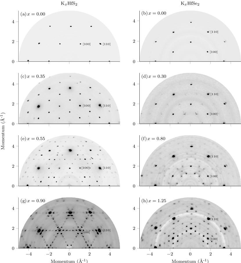
At a doping level of 0.35, HfS2 exhibits a clear superstructure [Fig. 5 (c)] where refers to the lattice parameter for the undoped material in the -plane. This is similar to what has been observed in alkali metal doped MoS2 where this diffraction pattern is caused by a distorted host lattice referred to as structure Habenicht et al. ; Fang et al. (2019). It also fits to the superstructure used for our DFT calculations, see Fig. 14 (e).
However, we were not able to index the Bragg peaks associated with the [11] reciprocal lattice points for that potassium concentration [Fig. 6 (c)]. This indicates a high degree of disorder along the -direction. It appears that the unit cell is not uniformly limited to only one molecular layer. Consequently, it is unlikely that the in-plane superstructure is caused by the occurrence of a crystal structure. Additional potassium () lead to a significant reduction in the intensity of the pattern and the appearance of additional diffraction spots in the -plane [Fig. 5 (e)]. The measurements of the [11] diffraction spots [Fig. 6 (e)], however, can be indexed which shows a restored order along the -axis with one layer per unit cell which is retained for all higher doping levels. This finding justifies the use of the same, smallest possible, periodicity in -direction in our DFT calculations. The reduced peak distances signify a considerable lattice expansion perpendicular to the planes. At the highest achieved alkali metal concentration of , the in-plane diffraction pattern is rearranged again to show mainly five diffraction peaks the lines between the main host lattice spots [Fig. 5 (g)].
The intercalation of HfSe2 resulted in weak multi-peak clusters distributed in a manner at [Fig. 5 (d)]. At the same time, the crystal becomes inhomogeneous in the -direction [Fig. 6 (d)] which permanently reverts back to a order at with increased lattice parameter [Fig. 6 (f)]. Nevertheless, the in-plane diffraction pattern undergoes further changes [Fig. 5 (f)] until it settles at a superstructure for [Fig. 5 (h)].
Given the almost continuous, doping level-dependent change of the diffraction patterns in the -plane, it is unlikely that this behavior is caused by structural changes in the host crystals. Such phase changes have been reported for MoS2 where the Fermi level separates the fully occupied orbital from the other orbitals leading to a structural instability upon electron doping Kertesz and Hoffmann (1984); Enyashin et al. (2011); Enyashin and Seifert (2012); Chhowalla et al. (2013); Voiry et al. (2015); Gao et al. (2015). As described above, the metal orbitals in the hafnium compounds are initially unoccupied. Consequently, there is no reason to believe that the initial filling will result in a change of the atomic coordination. Instead, the change in the Bragg peak positions appears to be caused by the ordering of the potassium atoms which rearrange themselves depending on their concentration. Moreover, a structural phase change has not been reported or predicted in the literature. Calculations for lithium-intercalated ZrS2, which closely resembles HfS2, indicate no significant structural distortions Zhao et al. (2019).
The intercalation affected the planar lattice parameters only slightly by changing them by not more than (not shown). In contrast, the -constants increased by () which is approximately the thickness of one potassium layer. The details are listed in Table 1. These percentage changes are similar to those observed in potassium-intercalated MoS2 Habenicht et al. ; Somoano et al. (1973); Ren et al. (2017); Rüdorff (1965); Habenicht et al. and TaSe2 König et al. (2012). The data show that the expansion is slightly reversed at high doping levels, a fact also reported for tantalum diselenide König et al. (2012). The inter-planar widening is largely due to the size of the potassium atoms which move into the Van-der-Waals gaps spreading the comparatively rigid molecular crystal planes apart from each other. That process has a large effect on the layer spacing even at low alkali metal concentration but levels out quickly. However, the interlayer bonding grows with increasing doping levels because of the larger number of electrons in the conduction band. This counteracts the expansion at larger values of . A systematic comparison between experimental and DFT lattice constants is presented in Fig. 4. The out-of-plane lattice parameters are largest for before they begin to contract again. The calculated expansion percentages agree very well with the experimentally observed values.
It should be mentioned that x-ray measurements performed by Whittingham and Gamble Whittingham and Gamble Jr (1975) found a unit cell spanning 3 molecular layers for lithium-intercalated HfS2 which is in surprising contrast to our results. We assume that those studies were done on samples with low intercalation levels still showing some degree of disorder.
IV.2 Semiconductor-to-Metal Transition
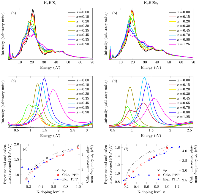
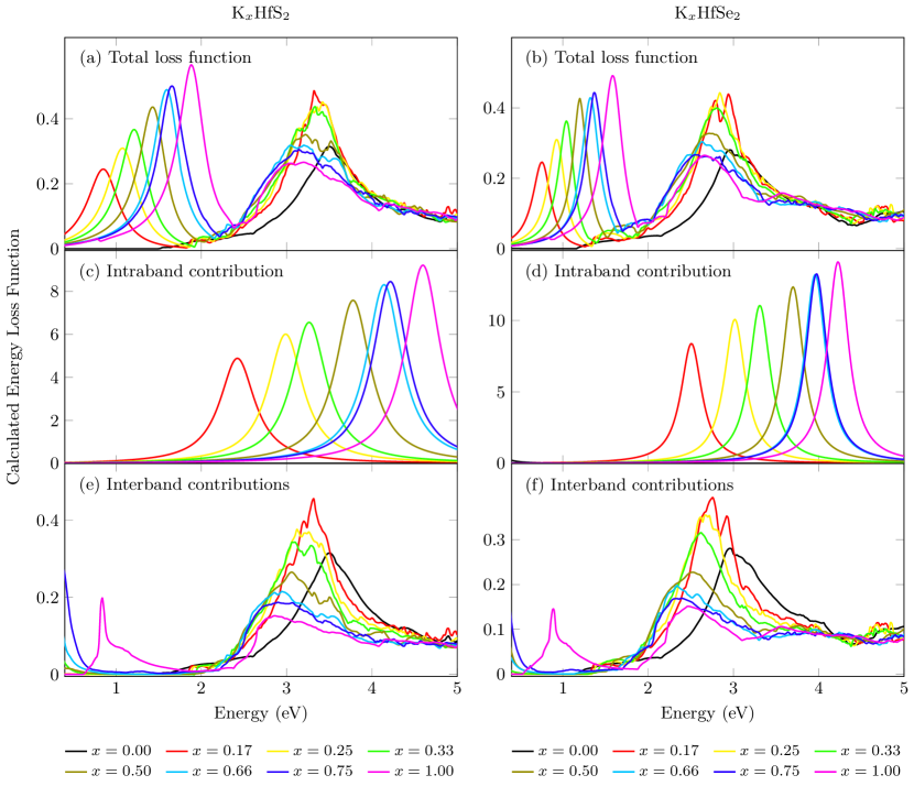
Fig. 7 (a) and (b) show the energy-loss spectra for hafnium disulfide and diselenide for a number of intercalation levels acquired at a momentum transfer value of parallel to the -direction. Because of the isotropy of the spectra in all directions at such small |q|, it is not necessary to show the data for the -direction as well. The spectra are dominated by the volume plasmons, the collective oscillations of all valence electrons. They are centered around for the undoped compounds [black plots in Fig. 7 (a) and (b)]. The features between and represent interband transitions Bell and Liang (1976). Hafnium core level excitations account for the peaks at and . There are also stimulations of the Hf states between and in both materials Bell and Liang (1976) that are superimposed on the effects of multiple scattering. For increasing doping levels, the volume plasmon peaks become more jagged and a feature forms at arising from K core levels.
In the low energy region, the spectra for the undoped crystals [black plots in Fig. 7 (c) and (d)] display band gaps followed by excitonic transitions Habenicht et al. (2018). As potassium is added, new features begin to form initially around . They shift to higher energies and rise in intensity as the K-concentration is increased before their intensity declines again while the peaks become broader. The fact that those new excitations develop in the energy region of the former band gaps and as a result of the intercalation with an electron donor suggests that they represent charge carrier plasmons and that semiconductor-to-metal transitions have occurred. The same phenomenon has been observed in K-intercalated WSe2 Ahmad et al. (2017) which is also a native semiconductor. The transition can also be seen in the shift of the Fermi energy in the calculated density of states leading to partially filled conduction bands (see Fig. 15 in Appendix VI).
Closer inspection of the DOS depicted in Fig. 15 reveals that, for all cases with , the conduction band bottom is characterized by a jump-like onset followed by an almost constant DOS up to the Fermi level and beyond. This means, the related systems host a quasi-twodimensional (2D) electron gas at the Fermi level. Given the observed thermodynamic stability for , the title systems could form a platform for investigations on a 2D electron gas with densities of electrons per cm2. We note that, a quasi-2D electronic structure may seem natural for the given anisotropic structure. However, at higher doping levels, van-Hove singularities other than 2D-like signal a 3D electronic structure close to the Fermi level (Fig. 15 o, p).
Let us turn back our attention to the EELS data. It is unusual that such spectra assume the shape of a double peak as can be seen for HfS2 at and 0.30. The two maxima are at and [Fig. 7 (c)]. For HfSe2 they are located at and for [Fig. 7 (d)]. Moreover, no plasmon peak forms in the energy region between the two peaks for any of the investigated doping levels. All other peak maxima are located either below or above those energies. This behavior can also be seen in Fig. 7 (e) and (f) where the plasmon peak positions (PPP) are plotted against the doping concentrations. In HfS2, the energetically higher peak forms first before the double feature appears at higher . In contrast, the energetically lower lying peak develops before the occurrence of the second one in hafnium diselenide. This raises the question why plasmon formation is not observed in the energy range between the two peaks. Possible reasons could be a phase change at particular doping levels or certain arrangements of the potassium ions in the host lattices. Besides the peak-splitting, the plasmon energies appear to remain relatively constant until a certain K-concentration is exceeded after which the peak energy positions increase.
To gain a better understanding of the reasons for those two observations, we calculated the formation energies per formula unit (f.u.) of the compounds for selected alkali metal concentrations.
| (4) |
with denoting the energy per f.u. of the doped chalcogenide (Ch = S, Se); and denoting the energies per f.u. of the reference systems bcc Potassium and HfCh2, respectively. The results are summarized in Fig. 8. The concave slope of the plots for doping levels up to indicates that a homogeneous doped phase is unstable below that potassium concentration. In contrast, the slope is convex for higher alkali metal concentrations implying that all structures considered in the simulations with are low-temperature stable against decomposition into structures with different doping levels. We note that the DFT calculations were carried out for bulk systems. Experimental data were obtained for films and could be slightly influenced by surface/interface effects, or by kinetics.
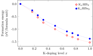
The suggested thermodynamic instability of low potassium concentrations could explain the fact that the plasmon position is relatively unchanged during the initial doping steps. If the amount of alkali metal is not sufficient to saturate the whole crystal uniformly at a thermodynamically stable concentration, domains will form to accommodate the potassium at the smallest stable concentration. As more potassium is added, the volume of the already intercalated regions increases at the expense of the pristine domains whose volume shrinks. The potassium concentration and, consequently, the density of the supplied conduction electrons remains constant in the intercalated domains during this process. This conduction electron density determines the unscreened plasmon frequency according to Equ. 2a. The screened plasmon frequency changes almost proportionally to . Their relation can be seen by comparing the positions of screened and unscreened plasmon frequencies obtained from DFT calculations in Fig. 7 (e) and (f). Consequently, the experimental plasmon peak position, which is close to the screened plasmon frequency, changes almost proportionally to the square root of the charge carrier density. Therefore, the relative stability of the plasmon peak position in the EELS spectra is an indication of a constant potassium concentration. In KxHfS22, this is the case up to and in KxHfSe2 up to . Before those points, the calculated potassium concentrations represent the average concentrations across the whole samples and not the concentration in the intercalated domains. The expansion of the intercalated domains leads to an enhancement of the plasmon intensities in Fig. 7 (c) and (d). Once the whole film has reached the minimum stable concentration, the doping level and the plasmon energy position increase smoothly as more potassium is provided. It is interesting that in contrast to those observations, WSe2 Ahmad et al. (2017), KxCuPc Flatz et al. (2007), and K2MnPc Mahns et al. (2011) permit only one particular potassium stoichiometry causing the plasmon peak position to be almost unchanged during the intercalation steps. On the other hand, the metallic TMDCs TaSe2, TaS2, NbSe2 and NbS2 appear to accept any alkali metal concentration König et al. (2012); Müller et al. (2016).
We used the FPLO code to calculate the energy loss spectra for different doping levels to determine if they would reproduce the experimental results. The calculated plots, which are presented in Fig. 9 (a) and (b), show a single peak moving to higher energies with increasing doping level. A peak splitting of the kind seen in the measured data cannot be identified. The emergence of the spectral double features at certain doping levels most likely arises from the temporary formation of two domains with differing doping concentrations that depart significantly from the thermodynamic equilibrium. Those domains are different from the ones described in the preceding paragraph which exist in equilibrium conditions. This additional kinematic effect may be caused by the experimental process where just one side of the crystal is exposed to the potassium stream during the intercalation leading to initially inhomogeneous alkali metal distributions. Such effects cannot entirely be prevented even though the samples were annealed after each intercalation step to minimize such issues. This reasoning is supported by the fact that the energetically higher one of the two peaks in KxHfSe2 at disappeared after longer electron beam exposure. The energy supplied by the beam may have induced a further migration of the potassium atoms and a more uniform distribution resulting in an equalization of the two regions. Another observation corroborating this assumption is that the double features exist only for doping levels for which the crystals display significant disorder in the -direction (see Sec. IV.1).
We computed the intraband and interband contributions to the loss function using FPLO. The intraband parts reflect the unscreened plasmons as presented in Fig. 9 (c) and (d). Just like the screened plasmon peaks, the unscreened plasmon features shift to higher energies with increasing and show no unusual behavior. For the undoped materials, the interband contributions in Fig. 9 (e) and (f) exhibit the expected band gaps followed by the exciton signatures. At , weak interband transitions begin to emerge near . Stronger excitations occur close to for . Nevertheless, the interband excitations are relatively weak compared to the intraband excitations. This verifies that the peaks in the loss function below are largely plasmonic in nature and that the same is true for the corresponding features in the experimental loss spectra.
IV.3 Unscreened Charge Carrier Plasmon Frequency
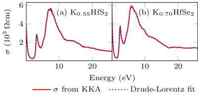
Because of their significance, we calculated the unscreened charge carrier plasmon frequencies from the measured EELS data. To extract the experimental values, it was necessary to separate the plasmons from the single particle excitations in the EELS spectra. For that purpose, the data for K0.55HfS2 and for K0.70HfSe2 measured in the energy range up to parallel to the direction were corrected for experimental artifacts by eliminating the elastic line, centered at , and the effects of multiple scatting according to the approach outlined in Refs. 77 and 86. A Kramers-Kronig analysis was performed on the outcomes based on the assumption that the samples were metallic. The resulting optical conductivity function [] is plotted in Fig. 10. It was fitted with one Drude and 14 Lorentz oscillators in the energy region up to to obtain the parameters in Equ. 1. The fitted values of stopped fluctuating for a larger number of oscillators. The complete fit parameter sets are provided in Table 5 in Appendix VI. The plots produced from them are displayed in Fig. 10. They show that the Drude-Lorentz model provides a good description of the optical conductivities. They also indicate that below is dominated by the charge carrier plasmon (Drude oscillator) while excitations of bound single particles (Lorentz oscillators) account mainly for the behavior at higher energies. The process lead to unscreened plasmon frequencies of for K0.55HfS2 and for K0.70HfSe2, respectively. Those values are somewhat lower than the theoretical numbers for comparable doping levels of for K0.50HfS2 and for K0.66HfSe2. However, the values are in a similar energy range and reasonably close given the approximations we have made.
IV.4 Plasmon Dispersion
Another interesting aspect of doping-induced plasmons is their dispersion. As stated above, the energy position of a plasmon peak in a spectrum corresponds to the unscreened plasmon frequency damped mainly by interband excitations. Besides an energy renormalization, the fundamental behavior of the screened plasmon peak position and the unscreened plasmon peak position is nearly the same Müller et al. (2017). This allows us to use the dispersion of the measured peak position as an approximation of the momentum dependence of the unscreened plasmon frequency. In an ideal metal, this frequency, and therefore the plasmon peak position, changes almost quadratically as function of momentum Nolting (2018); Nozières and Pines (1959):
| (5) |
where represents the Planck constant and the Fermi wave vector. However, experiments also found results that deviate from this ideal behavior. For example, the energy-momentum relations in TaS2, TaSe2 and NbSe2 are negative Schuster et al. (2009); van Wezel et al. (2011); Müller et al. (2016). They become positive and linear upon alkali metal intercalation Müller et al. (2016); König et al. (2013). Bi2Sr2CaCu2O8, on the other hand, has quadratic dispersion Nücker et al. (1991); Grigoryan et al. (1999).
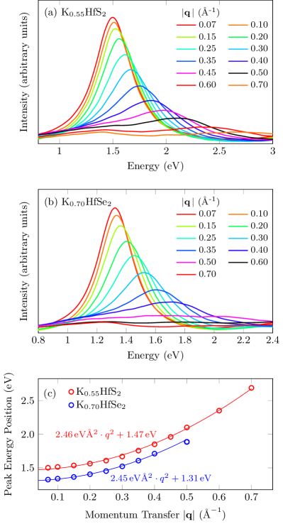
For each of the two materials under investigation, the doping levels with the most intense plasmon peaks ( for HfS2 and for HfSe2) were selected for an analysis of their momentum dependence. The spectra, measured for a range of momentum transfer values, are shown in Fig. 11 (a) and (b) and look very similar for both compounds. The peaks continuously shift to higher energies (up to and for HfS2 and HfSe2, respectively) and broaden as |q| increases. The plots of the peak energy positions vs. momentum transfer in Fig. 11 (c) reveal a quadratic dispersion which coincides with the expectations for plasmons in ideal metals according to Equ. 5.
Besides that strongly dispersing feature, a shoulder begins to emerge in the spectra for HfS2 near for [Fig. 11 (a)]. It develops into a separate peak at higher momentum transfer values and has a slight negative dispersion. The same phenomenon occurs in HfSe2 around [Fig. 11 (b)]. Those excitations represent interband transitions as can be seen from the calculated interband contributions to the loss functions in Fig. 9 (e) and (f). The latter exhibit such transitions in the energy region between and for higher potassium levels. Their intensities are weak so they cannot be distinguished from the stronger plasmons at low |q|. As the momentum transfer is raised, the plasmon peaks themselves peter out and shift away revealing the less dispersive single particle transitions.
IV.5 ARPES Spectra
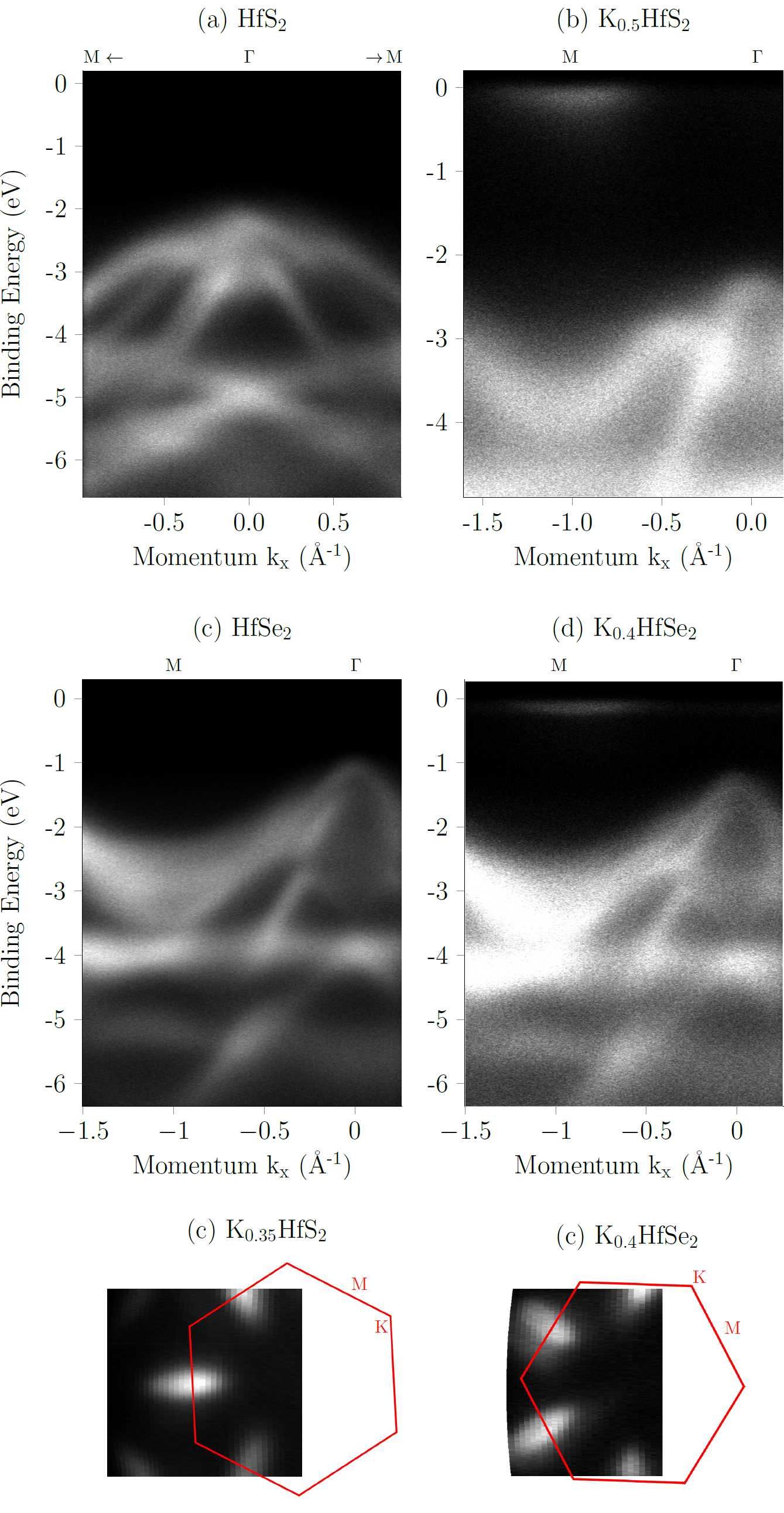
To confirm the occurrence of the semiconductor-to-metal transition and the validity of our computational results, we performed ARPES measurements on pristine and potassium-doped hafnium disulfide and diselenide. Similar experiments have been done before on pure Aretouli et al. (2015) and sodium-doped Mleczko et al. (2017); Eknapakul et al. (2018) HfSe2.
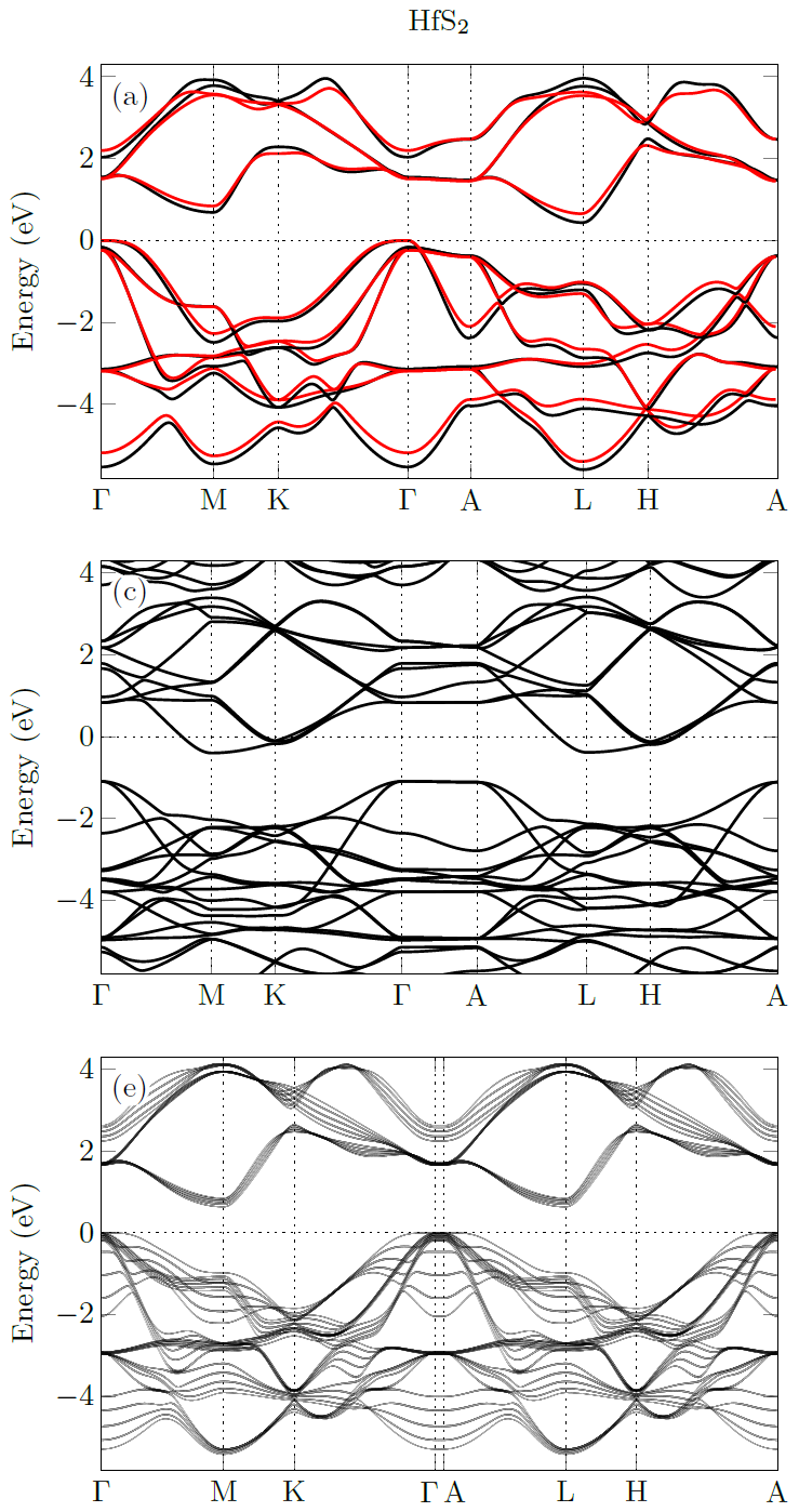
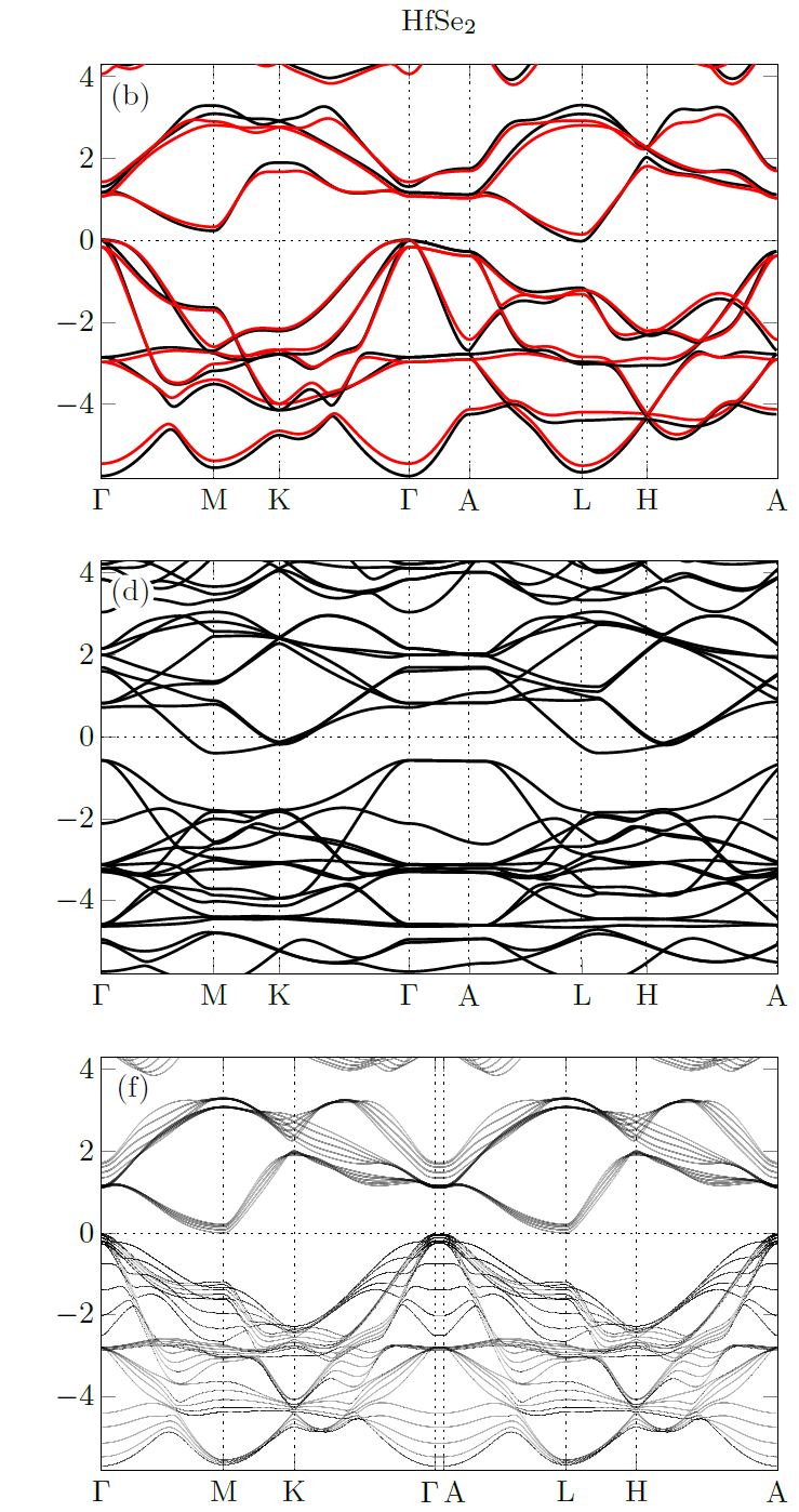
We calculated the bulk band structures for the undoped materials. Fig. 12 (a) and (b) display the results obtained from LDA-optimized as well as experimental lattice parameters (see Sec. IV.1 for the discussion of the experimentally determined lattice parameters). The two data sets show some moderate differences in the energy positions of parts of certain bands but no fundamental differences regarding the relative locations of the main features. The band structure for HfSe2 with optimized lattice parameters appears to be metallic even though the material is a semiconductor. The valence band maxima (VBM) are located at the point which agrees with theoretical results found by others Murray et al. (1972); Mattheiss (1973); Fong et al. (1976); Traving et al. (2001); Reshak and Auluck (2005); Jiang (2011). According to our calculations, the conduction band minima (CBM) are at the point. Because the local conduction band minima at the and points are energetically very close, it has been debated which one of them represents the absolute CBM with some calculations pointing to Jiang (2011); Mattheiss (1973), some to M Fong et al. (1976); Reshak and Auluck (2005), and some undetermined results Traving et al. (2001). Photoemission Traving et al. (2001) and optical transmission Terashima and Imai (1987) experiments suggest that the indirect gap is between and . The direct gap of HfS2 is in the range of according to conductivity and reflectivity measurements Bayliss and Liang (1982); Conroy and Park (1968) while absorption and differential transmission experiments report indirect band gaps of Camassel et al. (1977); Gaiser et al. (2004); Greenaway and Nitsche (1965); Yacobi et al. (1979). For HfSe2, reflectivity experiments observed a direct gap of Bayliss and Liang (1982). Absorption and scanning tunneling spectroscopy indicate an indirect gap of Yue et al. (2015); Greenaway and Nitsche (1965); Gaiser et al. (2004). Our calculations result in significantly smaller gaps. This is not unexpected given that LDA tends to underestimate those values Aryasetiawan and Gunnarsson (1998).
The theoretical bulk band structures [Fig. 12 (a) and (b)] deviate in some details from the ARPES spectra of the pristine samples in Fig. 13 (a) and (c). Note that the energy zero is placed at VBM in the calculated band structures. For example, the topmost band from the theoretical spectra appears to be shifted to a lower energy in the photoemission spectra leading to an additional shoulder. Moreover, there seem to be a number of diffuse, indistinguishable bands at between and for the sulfide compound and between and for the selenide one. One of the main factors contributing to the differences is that ARPES experiments are surface sensitive while the plots in Fig. 12 (a) and (b) were derived from calculations for bulk materials. To simulate the fact that the photoelectrons can escape only from positions very close to the sample surface, the band structures for a periodic slab of 5 molecular layers surrounded by vacuum were determined and presented in Fig. 12 (e) and (f). The bands are weighed by the distance of the photoelectron source from the sample surface according to Equ. 3 with an escape depth of . The resulting spectra resemble the experimental outcomes much better, in particular the valence band dispersion around and the multitude of bands below the VBM seen in the measured data. The outcome compares well to calculations performed by Aretouli et al. for free-standing 6-layer HfSe2 Aretouli et al. (2015). Nevertheless, the use of the bulk calculations is appropriate for the interpretation of the transmission EELS spectra because this method is bulk-sensitive.
The ARPES spectra for the K-doped samples are depicted in Fig. 13 (b) and (d). For , the influx of electrons from potassium atoms leads to a shift of the valence band maximum at from to below the Fermi energy in HfS2 indicating a rise of by . The shift creates an electron pocket at the Fermi energy representing the minimum of the now partially filled conduction band. The indirect gap between the VBM at and the CBM at amounts to . The position of the VBM is consistent with the calculated VBM at the points [see Fig. 12 (c)] obtained for an alkali metal concentration of , which is reasonably close to the actual doping level. The observation of this Fermi pocket is a clear sign of the semiconductor-to-metal transition.
Similarly, the energy maximum at decreases by to in HfSe2 for . The energy difference between the electron pocket at and the VBM is . This is slightly lower than Mleczko et al. observed for an ARPES investigation of sodium-intercalated HfSe2 Mleczko et al. (2017). As stated above, the calculated LDA band gaps in Fig. 12 (c) and (d) are smaller than the experimental values. The hexagonal arrangement and shape of electron pockets is visible in the momentum distribution curves shown in Fig. 13 (a) or (b).
V SUMMARIZING DISCUSSION
We used transmission electron energy loss spectroscopy and angle-resolved photoemission spectroscopy supported by DFT calculations to investigate the effect of potassium intercalation on bulk single crystals of HfS2 and HfSe2. Electron diffraction patterns showed a significant degree of disorder in the crystal structures for low doping concentrations. The structures become well-ordered again at alkali metal levels of and . At those points the materials show in-plane parameter changes of less than and out-of-plane lattice expansions of . Calculations indicate that the latter expansions reach their maximum at before they begin slightly to retract. Moreover, superstructures appear in the planes that we attribute to an ordered arrangement of the potassium ions minimizing their electrostatic (Madelung) energy.
The intercalation leads to the formation of a new feature in the energy-loss spectra below which can be identified as a charge carrier plasmon based on the calculated intraband contribution to the loss functions. It is a clear indication of a semiconductor-to-metal transition supported by computed DOSs and band structures. Its peak position remains relatively stable up to a certain potassium load. Close to this load, a double peak is observed and the doping-level dependence of the peak positions shows a clear gap. Related DFT calculations of the formation energies show that low potassium concentrations are thermodynamically unstable. These two observations indicate the formation of domains at low potassium load, i.e., the pristine phase coexists with a phase of lowest stable doping level . A possible reason for the instability of a low- phase could consist in the almost -independent effort to separate adjacent HfS2 or HfSe2 layers to accommodate potassium atoms which is counterbalanced at higher by a gain in the binding energy of potassium that is roughly proportional to . Yet higher doping concentrations results in a convex formation energy, Fig. 8, due to growing electrostatic repulsion among the dopands. As soon as a sufficient amount of potassium is intercalated to saturate the hole crystal with the minimum stable concentration, the potassium stoichiometry increases continuously for subsequent intercalation steps. This is reflected in a square-root like increase of the plasmon energy position.
The plasmons exhibit a quadratic momentum dispersion which leads to the revelation of weak interband transitions in the same energy region at larger -values.
ARPES measurements on the intercalated compounds show electron pockets from the conduction band corroborating the transition to metallic behavior.
Inspection of the calculated DOS and band structure revealed that the conduction band bottom hosts an almost ideal 2D electron gas for , with an approximate density of electrons per cm2.
Acknowledgements.
We thank R. Hübel, S. Leger, M. Naumann, F. Thunig and U. Nitzsche for their technical assistance. R. Schuster and C. Habenicht are grateful for funding from the IFW excellence program.References
- McTaggart and Wadsley (1958) F. K. McTaggart and A. D. Wadsley, Aust. J. Chem. 11, 445 (1958).
- Greenaway and Nitsche (1965) D. L. Greenaway and R. Nitsche, J. Phys. Chem. Solids 26, 1445 (1965).
- Conroy and Park (1968) L. E. Conroy and K. C. Park, Inorg. Chem. 7, 459 (1968).
- Bayliss and Liang (1982) S. C. Bayliss and W. Y. Liang, J. Phys. C: Solid State Phys. 15, 1283 (1982).
- Fiori et al. (2014) G. Fiori, F. Bonaccorso, G. Iannaccone, T. Palacios, D. Neumaier, A. Seabaugh, S. K. Banerjee, and L. Colombo, Nat. Nanotechnol. 9, 768 (2014).
- Mleczko et al. (2017) M. J. Mleczko, C. Zhang, H. R. Lee, H.-H. Kuo, B. Magyari-Köpe, R. G. Moore, Z.-X. Shen, I. R. Fisher, Y. Nishi, and E. Pop, Sci. Adv. 3, e1700481 (2017).
- Kanazawa et al. (2016) T. Kanazawa, T. Amemiya, A. Ishikawa, V. Upadhyaya, K. Tsuruta, T. Tanaka, and Y. Miyamoto, Sci. Rep. 6, 22277 (2016).
- Kang et al. (2015) M. Kang, S. Rathi, I. Lee, D. Lim, J. Wang, L. Li, M. A. Khan, and G.-H. Kim, Appl. Phys. Lett. 106, 143108 (2015).
- Kang et al. (2017) M. Kang, S. Rathi, I. Lee, L. Li, M. A. Khan, D. Lim, Y. Lee, J. Park, S. J. Yun, D.-H. Youn, C. Jun, and G.-H. Kim, Nanoscale 9, 1645 (2017).
- Xu et al. (2016) K. Xu, Y. Huang, B. Chen, Y. Xia, W. Lei, Z. Wang, Q. Wang, F. Wang, L. Yin, and J. He, Small 12, 3106 (2016).
- Chae et al. (2016) S. H. Chae, Y. Jin, T. S. Kim, D. S. Chung, H. Na, H. Nam, H. Kim, D. J. Perello, H. Y. Jeong, T. H. Ly, et al., ACS nano 10, 1309 (2016).
- Chang (2015) J. Chang, J. Appl. Phys. 117, 214502 (2015).
- Fu et al. (2017) L. Fu, F. Wang, B. Wu, N. Wu, W. Huang, H. Wang, C. Jin, L. Zhuang, J. He, L. Fu, and Y. Liu, Adv. Mater. 29, 1700439 (2017).
- Nie et al. (2017) X.-R. Nie, B.-Q. Sun, H. Zhu, M. Zhang, D.-H. Zhao, L. Chen, Q.-Q. Sun, and D. W. Zhang, ACS Appl. Mater. Interfaces 9, 26996 (2017).
- Kaur et al. (2018) H. Kaur, S. Yadav, A. K. Srivastava, N. Singh, S. Rath, J. J. Schneider, O. P. Sinha, and R. Srivastava, Nano Res. 11, 343 (2018).
- Gong et al. (2013) C. Gong, H. Zhang, W. Wang, L. Colombo, R. M. Wallace, and K. Cho, Appl. Phys. Lett. 103, 053513 (2013).
- Xu et al. (2015) K. Xu, Z. Wang, F. Wang, Y. Huang, F. Wang, L. Yin, C. Jiang, and J. He, Adv. Mater. 27, 7881 (2015).
- De Sanctis et al. (2018) A. De Sanctis, I. Amit, S. P. Hepplestone, M. F. Craciun, and S. Russo, Nat. Commun. 9, 1652 (2018).
- Yin et al. (2016) L. Yin, K. Xu, Y. Wen, Z. Wang, Y. Huang, F. Wang, T. A. Shifa, R. Cheng, H. Ma, and J. He, Appl. Phys. Lett. 109, 213105 (2016).
- Zheng et al. (2016) B. Zheng, Y. Chen, Z. Wang, F. Qi, Z. Huang, X. Hao, P. Li, W. Zhang, and Y. Li, 2D Mater. 3, 035024 (2016).
- Yan et al. (2017) C. Yan, L. Gan, X. Zhou, J. Guo, W. Huang, J. Huang, B. Jin, J. Xiong, T. Zhai, and Y. Li, Adv. Funct. Mater. 27, 1702918 (2017).
- Wang et al. (2018) D. Wang, X. Zhang, G. Guo, S. Gao, X. Li, J. Meng, Z. Yin, H. Liu, M. Gao, L. Cheng, J. You, and R. Wang, Adv. Mater. 30, 1803285 (2018).
- Mattinen et al. (2019) M. Mattinen, G. Popov, M. Vehkamäki, P. J. King, K. Mizohata, P. Jalkanen, J. Räisänen, M. Leskelä, and M. Ritala, Chem. Mater. 31, 5713 (2019).
- Gaiser et al. (2004) C. Gaiser, T. Zandt, A. Krapf, R. Serverin, C. Janowitz, and R. Manzke, Phys. Rev. B 69, 075205 (2004).
- Singh et al. (2016) D. Singh, S. K. Gupta, Y. Sonvane, A. Kumar, and R. Ahuja, Catal. Sci. Technol. 6, 6605 (2016).
- Terashima and Imai (1987) K. Terashima and I. Imai, Solid State Commun. 63, 315 (1987).
- Mattheiss (1973) L. Mattheiss, Phys. Rev. B 8, 3719 (1973).
- Beal et al. (1972) A. Beal, J. Knights, and W. Liang, J. Phys. C: Solid State Phys. 5, 3531 (1972).
- Lucovsky et al. (1973) G. Lucovsky, R. M. White, J. A. Benda, and J. F. Revelli, Phys. Rev. B 7, 3859 (1973).
- Hughes and Liang (1977) H. Hughes and W. Liang, J. Phys. C: Solid State Phys. 10, 1079 (1977).
- Fong et al. (1976) C. Fong, J. Camassel, S. Kohn, and Y. Shen, Phys. Rev. B 13, 5442 (1976).
- Borghesi et al. (1984a) A. Borghesi, B. Guizzetti, L. Nosenzo, E. Reguzzoni, A. Stella, and F. Levy, Il Nuovo Cimento D 4, 141 (1984a).
- Borghesi et al. (1984b) A. Borghesi, M. Geddo, G. Guizzetti, E. Reguzzoni, A. Stella, and F. Lévy, Phys. Rev. B 29, 3167 (1984b).
- Borghesi et al. (1986) A. Borghesi, C. Chen-jia, G. Guizzetti, L. Nosenzo, E. Reguzzoni, A. Stella, and F. Lévy, Phys. Rev. B 33, 2422 (1986).
- Shepherd and Williams (1974) F. R. Shepherd and P. M. Williams, J. Phys. C: Solid State Phys. 7, 4416 (1974).
- Jakovidis et al. (1987) G. Jakovidis, J. Riley, J. Liesegang, and R. Leckey, J. Electron Spectrosc. Relat. Phenom. 42, 275 (1987).
- Kreis et al. (2000) C. Kreis, M. Traving, R. Adelung, L. Kipp, and M. Skibowski, Appl. Surf. Sci. 166, 17 (2000).
- Traving et al. (2001) M. Traving, T. Seydel, L. Kipp, M. Skibowski, F. Starrost, E. E. Krasovskii, A. Perlov, and W. Schattke, Phys. Rev. B 63, 035107 (2001).
- Aretouli et al. (2015) K. Aretouli, P. Tsipas, D. Tsoutsou, J. Marquez-Velasco, E. Xenogiannopoulou, S. Giamini, E. Vassalou, N. Kelaidis, and A. Dimoulas, Appl. Phys. Lett. 106, 143105 (2015).
- Hodul and Stacy (1984) D. T. Hodul and A. M. Stacy, J. Solid State Chem. 54, 438 (1984).
- Iwasaki et al. (1982) T. Iwasaki, N. Kuroda, and Y. Nishina, J. Phys. Soc. Jpn. 51, 2233 (1982).
- Ibáñez et al. (2018) J. Ibáñez, T. Woźniak, F. Dybala, R. Oliva, S. Hernández, and R. Kudrawiec, Sci. Rep. 8, 12757 (2018).
- Najmaei et al. (2018) S. Najmaei, M. R. Neupane, B. M. Nichols, R. A. Burke, A. L. Mazzoni, M. L. Chin, D. A. Rhodes, L. Balicas, A. D. Franklin, and M. Dubey, Small 14, 1703808 (2018).
- Roubi and Carlone (1988) L. Roubi and C. Carlone, Phys. Rev. B 37, 6808 (1988).
- Cruz et al. (2018) A. Cruz, Z. Mutlu, M. Ozkan, and C. S. Ozkan, MRS Commun. 8, 1191 (2018).
- Cingolani et al. (1988) A. Cingolani, M. Lugarà, and F. Lévy, Phys. Scr. 37, 389 (1988).
- Zheng et al. (1989) X.-G. Zheng, H. Kuriyaki, and K. Hirakawa, J. Phys. Soc. Jpn. 58, 622 (1989).
- McTaggart (1958) F. K. McTaggart, Aust. J. Chem. 11, 471 (1958).
- Radhakrishnan and Mohanan Pilla (2008) K. Radhakrishnan and K. Mohanan Pilla, Asian J. Chem. 20, 3774 (2008).
- Bell and Liang (1976) M. Bell and W. Liang, Adv. Phys. 25, 53 (1976).
- Habenicht et al. (2018) C. Habenicht, L. Sponza, R. Schuster, M. Knupfer, and B. Büchner, Phys. Rev. B 98, 155204 (2018).
- Murray et al. (1972) R. Murray, R. Bromley, and A. Yoffe, J. Phys. C: Solid State Phys. 5, 746 (1972).
- Bullett (1978) D. W. Bullett, J. Phys. C: Solid State Phys. 11, 4501 (1978).
- Zhang et al. (2014) W. Zhang, Z. Huang, W. Zhang, and Y. Li, Nano Res. 7, 1731 (2014).
- Lebègue et al. (2013) S. Lebègue, T. Björkman, M. Klintenberg, R. M. Nieminen, and O. Eriksson, Phys. Rev. X 3, 031002 (2013).
- Eknapakul et al. (2018) T. Eknapakul, I. Fongkaew, S. Siriroj, W. Jindata, S. Chaiyachad, S.-K. Mo, S. Thakur, L. Petaccia, H. Takagi, S. Limpijumnong, et al., Phys. Rev. B 97, 201104 (2018).
- Reshak and Auluck (2005) A. H. Reshak and S. Auluck, Physica B 363, 25 (2005).
- Zhao et al. (2017) Q. Zhao, Y. Guo, K. Si, Z. Ren, J. Bai, and X. Xu, Phys. Status Solidi B 254, 1700033 (2017).
- Jaiswal et al. (2018) H. N. Jaiswal, M. Liu, S. Shahi, F. Yao, Q. Zhao, X. Xu, and H. Li, Semicond. Sci. Technol. 33, 124014 (2018).
- Yacobi et al. (1979) B. G. Yacobi, F. W. Boswell, and J. M. Corbett, J. Phys. C: Solid State Phys. 12, 2189 (1979).
- Iwasaki et al. (1983) T. Iwasaki, N. Kuroda, and Y. Nishina, Synth. Met. 6, 157 (1983).
- Pleshchev et al. (2011) V. Pleshchev, N. Baranov, D. Shishkin, A. Korolev, and A. Gorlov, Phys. Solid State 53, 2054 (2011).
- Dines (1975) M. B. Dines, Mater. Res. Bull. 10, 287 (1975).
- Whittingham and Gamble Jr (1975) M. S. Whittingham and F. R. Gamble Jr, Mater. Res. Bull. 10, 363 (1975).
- Õnuki et al. (1982) Y. Õnuki, R. Inada, S. Tanuma, S. Yamanaka, and H. Kamimura, J. Phys. Soc. Jpn. 51, 880 (1982).
- Beal and Nulsen (1981) A. Beal and S. Nulsen, Philos. Mag. B 43, 965 (1981).
- Camassel et al. (1977) J. Camassel, S. Kohn, Y. R. Shen, and F. Lévy, Il Nuovo Cimento B 38, 185 (1977).
- Nozières and Pines (1959) P. Nozières and D. Pines, Phys. Rev. 113, 1254 (1959).
- Raether (2006) H. Raether, Excitation of Plasmons and Interband Transitions by Electrons, Springer Tracts in Modern Physics (Springer Berlin Heidelberg, 2006).
- Müller et al. (2016) E. Müller, B. Büchner, C. Habenicht, A. König, M. Knupfer, H. Berger, and S. Huotari, Phys. Rev. B 94, 035110 (2016).
- König et al. (2012) A. König, K. Koepernik, R. Schuster, R. Kraus, M. Knupfer, B. Büchner, and H. Berger, Europhys. Lett. 100, 27002 (2012).
- König et al. (2013) A. König, R. Schuster, M. Knupfer, B. Büchner, and H. Berger, Phys. Rev. B 87, 195119 (2013).
- Ahmad et al. (2017) M. Ahmad, E. Müller, C. Habenicht, R. Schuster, M. Knupfer, and B. Büchner, J. Phys.: Condens. Matter 29, 165502 (2017).
- (74) C. Habenicht, A. Lubk, R. Schuster, M. Knupfer, and B. Büchner, Submitted for publication .
- Sturm (1993) K. Sturm, Z. Naturforsch. A 48a, 233 (1993).
- Note (1) Please note that the terms energy and frequency are used synonymously in the work ().
- Fink (1989) J. Fink, Adv. Electron El. Phys. 75, 121 (1989).
- Roth et al. (2014) F. Roth, A. König, J. Fink, B. Büchner, and M. Knupfer, J. Electron Spectrosc. Relat. Phenom. 195, 85 (2014).
- Somoano et al. (1973) R. Somoano, V. Hadek, and A. Rembaum, J. Chem. Phys. 58, 697 (1973).
- Zhang et al. (2015) R. Zhang, I.-L. Tsai, J. Chapman, E. Khestanova, J. Waters, and I. V. Grigorieva, Nano Lett. 16, 629 (2015).
- Wang et al. (2014) X. Wang, X. Shen, Z. Wang, R. Yu, and L. Chen, ACS Nano 8, 11394 (2014).
- Cheng et al. (2014) Y. Cheng, A. Nie, Q. Zhang, L.-Y. Gan, R. Shahbazian-Yassar, and U. Schwingenschlogl, ACS Nano 8, 11447 (2014).
- Huang et al. (2018) Q. Huang, L. Wang, Z. Xu, W. Wang, and X. Bai, Sci. China Chem. 61, 222 (2018).
- Li (2017) Y. Li, Plasmonic optics: Theory and applications (SPIE Press Bellingham, 2017).
- Hecht (2017) E. Hecht, Optics, 4th ed. (Addison Wesley, 2017).
- Schuster et al. (2009) R. Schuster, R. Kraus, M. Knupfer, H. Berger, and B. Büchner, Phys. Rev. B 79, 045134 (2009).
- Note (2) https://www.fplo.de/.
- Koepernik and Eschrig (1999) K. Koepernik and H. Eschrig, Phys. Rev. B 59, 1743 (1999).
- Richter et al. (2008) M. Richter, K. Koepernik, and H. Eschrig, in Condensed Matter Physics in the Prime of the 21st Century: Phenomena, Materials, Ideas, Methods (World Scientific, 2008) pp. 271–291.
- Perdew and Wang (1992) J. P. Perdew and Y. Wang, Phys. Rev. B 45, 13244 (1992).
- Jiang (2011) H. Jiang, J. Chem. Phys. 134, 204705 (2011).
- Seah and Dench (1979) M. P. Seah and W. A. Dench, Surf. Interface Anal. 1, 2 (1979).
- Friend and Yoffe (1987) R. Friend and A. Yoffe, Adv. Phys. 36, 1 (1987).
- Rimmington and Balchin (1974) H. P. B. Rimmington and A. A. Balchin, J. Mater. Sci. 9, 343 (1974).
- Fang et al. (2019) Y. Fang, X. Hu, W. Zhao, J. Pan, D. Wang, K. Bu, Y. Mao, S. Chu, P. Liu, T. Zhai, et al., J. Am. Chem. Soc. 141, 790 (2019).
- Kertesz and Hoffmann (1984) M. Kertesz and R. Hoffmann, J. Am. Chem. Soc. 106, 3453 (1984).
- Enyashin et al. (2011) A. N. Enyashin, L. Yadgarov, L. Houben, I. Popov, M. Weidenbach, R. Tenne, M. Bar-Sadan, and G. Seifert, J. Phys. Chem. C 115, 24586 (2011).
- Enyashin and Seifert (2012) A. N. Enyashin and G. Seifert, Comput. Theor. Chem. 999, 13 (2012).
- Chhowalla et al. (2013) M. Chhowalla, H. S. Shin, G. Eda, L.-J. Li, K. P. Loh, and H. Zhang, Nat. Chem. 5, 263 (2013).
- Voiry et al. (2015) D. Voiry, A. Mohite, and M. Chhowalla, Chem. Soc. Rev. 44, 2702 (2015).
- Gao et al. (2015) G. Gao, Y. Jiao, F. Ma, Y. Jiao, E. Waclawik, and A. Du, J. Phys. Chem. C 119, 13124 (2015).
- Zhao et al. (2019) T. Zhao, H. Shu, Z. Shen, H. Hu, J. Wang, and X. Chen, J. Phys. Chem. C 123, 2139 (2019).
- Ren et al. (2017) X. Ren, Q. Zhao, W. D. McCulloch, and Y. Wu, Nano Res. 10, 1313 (2017).
- Rüdorff (1965) W. Rüdorff, Chimia 19, 489 (1965).
- Flatz et al. (2007) K. Flatz, M. Grobosch, and M. Knupfer, J. Chem. Phys. 126, 214702 (2007).
- Mahns et al. (2011) B. Mahns, F. Roth, M. Grobosch, D. R. Zahn, and M. Knupfer, J. Chem. Phys. 134, 194504 (2011).
- Müller et al. (2017) E. Müller, B. Büchner, M. Knupfer, and H. Berger, Phys. Rev. B 95, 075150 (2017).
- Nolting (2018) W. Nolting, Theoretical Physics 9: Fundamentals of Many-body Physics, 2nd ed. (Springer International Publishing, 2018) p. 248.
- van Wezel et al. (2011) J. van Wezel, R. Schuster, A. König, M. Knupfer, J. van den Brink, H. Berger, and B. Büchner, Phys. Rev. Lett. 107, 176404 (2011).
- Nücker et al. (1991) N. Nücker, U. Eckern, J. Fink, and P. Müller, Phys. Rev. B 44, 7155 (1991).
- Grigoryan et al. (1999) V. G. Grigoryan, G. Paasch, and S.-L. Drechsler, Phys. Rev. B 60, 1340 (1999).
- Yue et al. (2015) R. Yue, A. T. Barton, H. Zhu, A. Azcatl, L. F. Pena, J. Wang, X. Peng, N. Lu, L. Cheng, R. Addou, S. McDonnell, L. Colombo, J. W. P. Hsu, J. Kim, M. J. Kim, R. M. Wallace, and C. L. Hinkle, ACS Nano 9, 474 (2015).
- Aryasetiawan and Gunnarsson (1998) F. Aryasetiawan and O. Gunnarsson, Rep. Prog. Phys. 61, 237 (1998).
VI APPENDIX
| Optimized atomic coordinates | ||||||
|---|---|---|---|---|---|---|
| Calculation parameters | Atom | x /a | y/b | z/c | ||
| 1. Bulk HfS2 (experimental lattice parameters): | ||||||
| Space group: (164) | Hf | 0 | 0 | 0 | ||
| -mesh for structure optimization: | S | 1/3 | -1/3 | 0.248 | ||
| -mesh for band structure/DOS/Optics: | ||||||
| Lattice parameters: | ||||||
| 2. Bulk HfS2 (optimized lattice parameters): | ||||||
| Space group: (164) | Hf | 0 | 0 | 0 | ||
| -mesh for structure optimization: | S | 1/3 | -1/3 | 0.256 | ||
| -mesh for band structure/DOS/Optics: | ||||||
| Lattice parameters: | ||||||
| 3. Bulk K0.17HfS2 (optimized lattice parameters): | ||||||
| Space group: (10) | Hf | 0 | 0 | 0 | ||
| -mesh for structure optimization: | Hf | 0 | -1/2 | -1/2 | ||
| -mesh for band structure/DOS/Optics: | Hf | 0 | -0.336 | 0 | ||
| Lattice parameters: | Hf | 0 | 0.170 | -1/2 | ||
| Axis angles: | S | -0.193 | -0.167 | -0.167 | ||
| S | 0.194 | -0.333 | -0.333 | |||
| S | -0.194 | -1/2 | -0.167 | |||
| S | -0.192 | 0 | 0.335 | |||
| K | 1/2 | 0 | 0 | |||
| 4. Bulk K0.25HfS2 (optimized lattice parameters): | ||||||
| Space group: (164) | Hf | 0 | 0 | 0 | ||
| -mesh for structure optimization: | Hf | 0 | -1/2 | 0 | ||
| -mesh for band structure/DOS/Optics: | S | 0.167 | -0.167 | 0.190 | ||
| Lattice parameters: | S | -1/3 | 1/3 | 0.189 | ||
| K | 0 | 0 | -1/2 | |||
| 5. Bulk K0.33HfS2 (optimized lattice parameters): | ||||||
| Space group: (162) | Hf | 0 | 0 | 0 | ||
| -mesh for structure optimization: | Hf | 1/3 | -1/3 | 0 | ||
| -mesh for band structure/DOS/Optics: | S | 0 | -0.334 | 0.191 | ||
| Lattice parameters: | K | 0 | 0 | -1/2 | ||
| 6. Bulk K0.50HfS2 (optimized lattice parameters): | ||||||
| Space group: (10) | Hf | 0 | 0 | 0 | ||
| -mesh for structure optimization: | Hf | 0 | 1/2 | -1/2 | ||
| -mesh for band structure/DOS/Optics: | S | -0.196 | 0 | -0.337 | ||
| Lattice parameters: | S | 0.196 | 1/2 | -0.164 | ||
| Axis angles: | K | -1/2 | 0 | 0 | ||
| 7. Bulk K0.66HfS2 (optimized lattice parameters): | ||||||
| Space group: (162) | Hf | 0 | 0 | 0 | ||
| -mesh for structure optimization: | Hf | 1/3 | -1/3 | 0 | ||
| -mesh for band structure/DOS/Optics: | S | 0 | -0.332 | 0.198 | ||
| Lattice parameters: | K | -1/3 | 1/3 | -1/2 | ||
| 8. Bulk K0.75HfS2 (optimized lattice parameters): | ||||||
| Space group: (164) | Hf | 0 | 0 | 0 | ||
| -mesh for structure optimization: | Hf | 0 | -1/2 | 0 | ||
| -mesh for band structure/DOS/Optics: | S | 0.166 | -0.166 | 0.198 | ||
| Lattice parameters: | S | -1/3 | 1/3 | 0.200 | ||
| K | -1/2 | 0 | -1/2 | |||
| 9. Bulk K0.83HfS2 (optimized lattice parameters): | ||||||
| Space group: (162) | Hf | 0 | 0 | 0 | ||
| -mesh for structure optimization: | Hf | -0.330 | -0.165 | 0 | ||
| Lattice parameters: | Hf | 1/2 | 1/2 | 0 | ||
| Hf | -1/3 | 1/3 | 0 | |||
| S | -0.500 | 0.333 | 0.196 | |||
| S | 0 | 0.333 | 0.201 | |||
| S | 0 | -0.167 | 0.204 | |||
| K | 0.349 | 0.175 | -1/2 | |||
| K | 1/2 | 1/2 | -1/2 | |||
| K | 0 | 0 | -1/2 | |||
| 10. Bulk K1.00HfS2 (optimized lattice parameters): | ||||||
| Space group: (164) | Hf | 0 | 0 | 0 | ||
| -mesh for structure optimization: | S | 1/3 | -1/3 | 0.202 | ||
| -mesh for band structure/DOS/Optics: | K | 0 | 0 | 1/2 | ||
| Lattice parameters: | ||||||
| 11. Surface HfS2 (5 structural unit cells and | ||||||
| vacuum): | ||||||
| space group: (164) | Hf | 0 | 0 | 0.250 | ||
| -mesh for band structure/DOS/Optics: | Hf | 0 | 0 | 0.375 | ||
| Lattice parameters: | Hf | 0 | 0 | 1/2 | ||
| S | 1/3 | -1/3 | 0.283 | |||
| S | 1/3 | -1/3 | 0.407 | |||
| S | 1/3 | -1/3 | -0.468 | |||
| S | 1/3 | -1/3 | -0.343 | |||
| S | 1/3 | -1/3 | -0.219 | |||
| Optimized atomic coordinates | ||||||
|---|---|---|---|---|---|---|
| Calculation parameters | Atom | x/a | y/b | z/c | ||
| 1. Bulk HfSe2 (experimental lattice parameters): | ||||||
| Space group: (164) | Hf | 0 | 0 | 0 | ||
| -mesh for structure optimization: | Se | 1/3 | -1/3 | 0.255 | ||
| -mesh for band structure/DOS/Optics: | ||||||
| Lattice parameters: | ||||||
| 2. Bulk HfSe2 (optimized lattice parameters): | ||||||
| Space group: (164) | Hf | 0 | 0 | 0 | ||
| -mesh for structure optimization: | Se | 1/3 | -1/3 | 0.262 | ||
| -mesh for band structure/DOS/Optics: | ||||||
| Lattice parameters: | ||||||
| 3. Bulk K0.17HfSe2 (optimized lattice parameters): | ||||||
| Space group: (10) | Hf | 0 | 0 | 0 | ||
| -mesh for structure optimization: | Hf | 0 | -1/2 | -1/2 | ||
| -mesh for band structure/DOS/Optics: | Hf | 0 | -0.337 | 0 | ||
| Lattice parameters: | Hf | 0 | 0.171 | -1/2 | ||
| Axis angles: | Se | -0.201 | -0.168 | -0.167 | ||
| Se | 0.203 | -0.334 | -0.332 | |||
| Se | -0.204 | -1/2 | -0.168 | |||
| Se | -0.199 | 0 | 0.337 | |||
| K | 1/2 | 0 | 0 | |||
| 4. Bulk K0.25HfSe2 (optimized lattice parameters): | ||||||
| Space group: (164) | Hf | 0 | 0 | 0 | ||
| -mesh for structure optimization: | Hf | 0 | -1/2 | 0 | ||
| -mesh for band structure/DOS/Optics: | Se | 0.167 | -0.167 | 0.196 | ||
| Lattice parameters: | Se | -1/3 | 1/3 | 0.195 | ||
| K | 0 | 0 | -1/2 | |||
| 5. Bulk K0.33HfSe2 (optimized lattice parameters): | ||||||
| Space group: (162) | Hf | 0 | 0 | 0 | ||
| -mesh for structure optimization: | Hf | 1/3 | -1/3 | 0 | ||
| -mesh for band structure/DOS/Optics: | Se | 0 | -0.335 | 0.197 | ||
| Lattice parameters: | K | 0 | 0 | 1/2 | ||
| 6. Bulk K0.50HfSe2 (optimized lattice parameters): | ||||||
| Space group: (10) | Hf | 0 | 0 | 0 | ||
| -mesh for structure optimization: | Hf | 0 | 1/2 | -1/2 | ||
| -mesh for band structure/DOS/Optics: | Se | -0.199 | 0 | -0.335 | ||
| Lattice parameters: | Se | 0.201 | 1/2 | -0.168 | ||
| Axis angles: | K | -1/2 | 0 | 0 | ||
| 7. Bulk K0.66HfSe2 (optimized lattice parameters): | ||||||
| Space group: (162) | Hf | 0 | 0 | 0 | ||
| -mesh for structure optimization: | Hf | 1/3 | -1/3 | 0 | ||
| -mesh for band structure/DOS/Optics: | Se | 0 | -0.332 | 0.199 | ||
| Lattice parameters: | K | -1/3 | 1/3 | 1/2 | ||
| 8. Bulk K0.75HfSe2 (optimized lattice parameters): | ||||||
| Space group: (164) | Hf | 0 | 0 | 0 | ||
| -mesh for structure optimization: | Hf | 0 | -1/2 | 0 | ||
| -mesh for band structure/DOS/Optics: | Se | 0.166 | -0.166 | 0.202 | ||
| Lattice parameters: | Se | -1/3 | 1/3 | 0.204 | ||
| K | -1/2 | 0 | -1/2 | |||
| 9. Bulk K0.83HfSe2 (optimized lattice parameters): | ||||||
| Space group: (162) | Hf | 0 | 0 | 0 | ||
| -mesh for structure optimization: | Hf | -0.330 | -0.165 | 0 | ||
| Lattice parameters: | Hf | -1/2 | -1/2 | 0 | ||
| Hf | -1/3 | 1/3 | 0 | |||
| Se | -0.499 | 0.333 | 0.200 | |||
| Se | 0 | 0.333 | 0.204 | |||
| Se | 0 | -0.167 | 0.207 | |||
| K | 0.348 | 0.174 | 1/2 | |||
| K | -1/2 | -1/2 | 1/2 | |||
| K | 0 | 0 | 1/2 | |||
| 10. Bulk K1.00HfSe2 (optimized lattice parameters): | ||||||
| Space group: (164) | Hf | 0 | 0 | 0 | ||
| -mesh for structure optimization: | Se | 1/3 | -1/3 | 0.203 | ||
| -mesh for band structure/DOS/Optics: | K | 0 | 0 | -1/2 | ||
| Lattice parameters: | ||||||
| 11. Surface HfSe2 (5 structural unit cells and | ||||||
| vacuum): | ||||||
| Space group: (164) | Hf | 0 | 0 | 0.245 | ||
| -mesh for band structure/DOS/Optics: | Hf | 0 | 0 | 0.373 | ||
| Lattice parameters: | Hf | 0 | 0 | -1/2 | ||
| Se | 1/3 | -1/3 | 0.279 | |||
| Se | 1/3 | -1/3 | 0.406 | |||
| Se | 1/3 | -1/3 | -0.467 | |||
| Se | 1/3 | -1/3 | -0.339 | |||
| Se | 1/3 | -1/3 | -0.212 | |||
| KxHfS2 | KxHfSe2 | ||||||||||
| Undoped () | Doped () | Undoped () | Doped () | ||||||||
| Miller | Momen- | Calculated | Momen- | Calculated | Momen- | Calculated | Momen- | Calculated | |||
| Index | tum | Unit Cell | tum | Unit Cell | tum | Unit Cell | tum | Unit Cell | |||
| -value | Transfer | Parameter | Transfer | Parameter | Transfer | Parameter | Transfer | Parameter | |||
| ([11]) | ca | ca | ca | ca | |||||||
| 0 | 3.47 | - | 3.49 | - | 3.35 | - | 3.33 | - | |||
| 1 | 3.63 | 5.76 | 3.58 | 7.93 | 3.51 | 5.93 | 3.41 | 8.26 | |||
| 2 | 4.09 | 5.77 | 3.85 | 7.75 | 3.92 | 6.14 | 3.66 | 8.19 | |||
| 3 | 4.76 | 5.77 | 4.24 | 7.85 | 4.55 | 6.12 | 4.05 | 8.18 | |||
| 4 | - | - | 4.75 | 7.81 | - | - | 4.50 | 8.31 | |||
| Average | 5.77 | 7.84 | 6.06 | 8.23 | |||||||
-
a
Calculation of unit cell parameter: where is the momentum transfer associated with the diffraction peak of the Miller index [11].
| Oscillator | Oscillator | K0.55HfS2 | K0.70HfSe2 | ||||
|---|---|---|---|---|---|---|---|
| index | Type | (eV) | (eV) | (eV) | (eV) | (eV) | (eV) |
| - | Drude | 0 | 0.37 | 3.55 | 0 | 0.25 | 3.89 |
| 1 | Lorentz | 3.14 | 0.33 | 1.61 | 2.2 | 0.14 | 0.56 |
| 2 | Lorentz | 3.34 | 0.36 | 1.95 | 2.37 | 0.23 | 1.11 |
| 3 | Lorentz | 3.6 | 0.46 | 1.69 | 2.53 | 0.28 | 1.95 |
| 4 | Lorentz | 3.95 | 0.98 | 2.38 | 2.68 | 0.24 | 1.51 |
| 5 | Lorentz | 5.32 | 1.45 | 2.87 | 2.85 | 0.43 | 1.99 |
| 6 | Lorentz | 6.2 | 0.8 | 2.32 | 3.19 | 0.69 | 2.28 |
| 7 | Lorentz | 6.68 | 0.19 | 0.61 | 3.66 | 0.49 | 0.87 |
| 8 | Lorentz | 6.95 | 1.78 | 6.61 | 4.42 | 1.3 | 2.81 |
| 9 | Lorentz | 7.55 | 0.31 | 0.96 | 5.81 | 1.98 | 7.28 |
| 10 | Lorentz | 7.85 | 0.17 | 0.68 | 7.39 | 3.71 | 9.71 |
| 11 | Lorentz | 8.34 | 2.84 | 7.87 | 9.75 | 1.64 | 2.68 |
| 12 | Lorentz | 10.26 | 3.33 | 5.11 | 12.83 | 7.76 | 9.66 |
| 13 | Lorentz | 14.14 | 5.31 | 6.12 | 19.93 | 4.94 | 3.87 |
| 14 | Lorentz | 20.74 | 23.72 | 13.05 | 25.64 | 10.29 | 8.66 |