Robust and Optimal Single-loop Voltage Controller for Grid-forming Voltage Source Inverters
Abstract
Design and implementation of an optimal and robust single-loop voltage controller is proposed for single-phase grid-forming voltage source inverter (VSI). The objective of the proposed controller is to have good reference tracking and disturbance rejection. Uncertain nature of loads can significantly alter system’s behavior, especially during heavily loaded conditions, and impose an uncertainty in the dynamic model. This deteriorates the robustness of the controller severely. -based controller design is proposed in this article to address this issue. The required objectives of the optimal controller are formulated after modeling the loads as uncertain element of the control system. Time-domain MATLAB/SIMULINK-based simulation study substantiates the fact that the resulting controller exhibits superior robustness in performance during varying loading conditions of VSI than that of the conventional multi-loop control architecture. OPAL-RT based controller hardware-in-the-loop (CHIL) simulations with low-cost controller are conducted to validate the computational footprint of the resulting controller.
Index Terms:
loop shaping, multiplicative uncertainty, robust control, voltage controller, voltage source inverter,I Introduction
During islanded mode of operation of AC microgrid, grid-forming voltage source inverters (VSI) play an essential role by maintaining a stable voltage and frequency of the network and supplying uninterrupted power to the loads in the absence of a stiff distribution grid. Both centralized (master-slave) and decentralized (droop-based) Level-1 control layer architecture have been proposed in order to meet the uninterrupted power supply to the loads in the network via generating a voltage reference for the Level-0 control layer [1]. In Level-0 control layer, a voltage controller is required to be designed for each grid-forming VSI so that the output voltage waveform of each VSI tracks the respective voltage reference signal [2].
Designing the voltage controller is essentially a multi-objective task. The design needs to primarily guarantee perfect reference tracking and good disturbance rejection which results in an output voltage with good regulation and low harmonic distortion in presence of various linear and non-linear loads. Additionally, the controllers are required to provide compensation to dynamic variations of the output current and improve the dynamic response [3]. It is also found that the unknown nature of the output loads can significantly alter the system behavior, especially during heavily loaded condition of VSI, that deteriorates the transient performance severely [4]. The controller is required to perform all the aforementioned multi-objective tasks under output load uncertainties. As a result, requirement of robust performance of the voltage controller warrants an essential criterion during design stage.
Numerous voltage control strategies are proposed in the literature during past decades for grid-forming VSIs. Most of the earlier control techniques are based on linear control theory with a single voltage control-loop scheme [5]. To further enhance the disturbance imposed by variations in input voltage and output current, a non-linear feed-forward loop is added in [6]. However, single-loop classical controllers experience poor transient response and limited stability margins [7]. To overcome these drawbacks, multiple-loop proportional-resonant (PR) and proportional-integral-differential (PID)-based classical control methods are proposed in [7, 8, 9, 10]. This common architecture has an internal current negative feedback loop, commanded by the error signal of the outer voltage regulation loop [3]. By introducing the inner current loop, the poles of the resonant filter can be decoupled to compensate the non-idealities of the inductor. Moreover, it facilitates an inherent over-current protection of the VSI. However, having an inner-loop current controller requires more sensors that increases the overall cost [11]. Moreover, classical controllers lack robustness in performance with output load uncertainties [9]. In [12, 13, 14], a lower order controller is designed using methodology by removing the higher order part of the internal model using repetitive control technique. However, in these approaches load uncertainty is not taken into account. A robust tuning strategy for PID-based double-loop lag–lead compensator for VSI is proposed in [15]. -based methodology is further explored in [16, 17, 18, 19] in order to design an optimal controller for VSIs with linear and non-linear load disturbances. However, both these works inherently adapt the multi-loop structure for voltage controller and load uncertainty is not considered during design. In [20], a sliding-mode control-based design for inner current loop and a mixed -based optimal design for outer voltage loop is proposed. A very similar design is proposed in [21] where linear matrix inequality (LMI)-based linear quadratic regulator (LQR) for inner current loop and mixed -based design for outer voltage loop are employed. Both these designs improve the transient response significantly in presence of uncertain filter parameters at the cost of added complexity in controllers. Moreover, uncertainty imposed by output loads is not taken into consideration while designing the controllers. [22] provides a robust optimal state-feedback controller based on the integration of optimal output regulation theory and back-stepping method where load is treated as a uncertain element. However, the impact of non-linear loads (various harmonic components) is not considered in this work. The primary contributions of this article are as follows:
-
1.
A simple robust and optimal (single-loop, low-cost) voltage controller for Level-0 control layer is proposed that can address the aforementioned limitations along with taking into account the uncertainties in load variations.
-
2.
It facilitates lower requirements of sensor measurements as opposed to other works in the literature without compromising in voltage regulation and disturbance rejection while guaranteeing robust performance.
Time-domain MATLAB/SIMULINK-based simulation with low-cost controller are performed in the validation stage of the proposed control.
II Problem Formulation
II-A Architecture of Grid-forming VSI
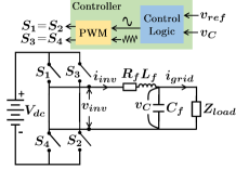
A single-phase grid-forming VSI terminated by a load, , is shown in Fig. 1LABEL:sub@fig:circ. The VSI is composed of a dc bus voltage, , four switching devices, -, and an filter with , as filter inductor and capacitor respectively. is the equivalent series resistance (ESR) of capturing parasitic element. The controller along with sinusoidal PWM switching technique generates the switching signals that result the output voltage. The dynamics of the VSI are described as:
| (1) | ||||
| (2) |
where signifies the average values of the corresponding variable over one switching cycle () [3]. Combining (1) and (2) and taking Laplace transformation, the open-loop output voltage dynamics of the grid-forming VSI is given as:
| (3) |
where
II-B Load Characteristics and Modeling
Characterizing the nature of the load is essential in the process of designing the controller. In this work, the load is modeled by a parallel combination of two components. First component is an admittance, , with unknown and elements, and can be defined as:
where, is a frequency dependent weighting function, capturing the nominal behavior, and defined as:
A normalized dynamic LTI uncertainty, , is defined to capture the uncertain behavior of load change such that
The value of and can be selected as and , where , , and are the rated output voltage, active, reactive power of the grid-forming VSI and nominal frequency of the network respectively. Another component of loads is a parallel combination of current sources consisting of both fundamental and harmonic components [23] and defined as
Therefore, of Fig. 1LABEL:sub@fig:circ can be characterized as
| (4) |
Remark.
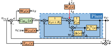
Multiplicative uncertainty in is used to shape the “worst-case” yet allowable output admittance of the grid-forming VSI. The exogenous disturbance signal, , captures the presence of non-linear loads as shown in Fig. 2LABEL:sub@control1.
II-C Impact of Load Uncertainty
Combining (3) and (II-B), system’s dynamic equation becomes
| (5) |
where,
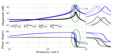
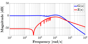
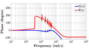
Clearly uncertainty in imposes uncertainty in both and as illustrated in Fig. 1LABEL:sub@fig:GvZd. It can be observed that the unknown load across VSI causes significant change in the plant dynamics, especially the effective resonant frequency of the system. This deteriorates the robust performance of the controller severely as well as overall system stability [4].
III Proposed Solution
III-A Objectives of the Designed Controller
The objective is to design a feedback control law through controller, as shown in Fig. 2LABEL:sub@control1, which generates a control signal, , such that, i) tracks , ii) effects of on is attenuated, iii) satisfies bandwidth limitations, and iv) recovers quickly after any sort of transients. Moreover, all aforementioned objectives need to be achieved with load uncertainty. In other words, it is necessary to provide the controller with enough robustness to deal with system uncertainty caused by load variation. These objectives are derived from acceptable standards on microgrid operation, IEEE Std-2030 [24], and power quality, IEEE Std-519[25].
III-B Design Procedure of the -based Controller
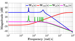
-based controller design provides a framework for addressing multiple objectives. Here, the design is based on the system structure presented in Fig. 2LABEL:sub@control1 where user-defined weighting transfer functions, , , and , are selected based on the aforementioned requirements. The brief guidelines for designing the weighting transfer functions are provided below.
III-B1 Selection of
To shape the sensitivity transfer function, the weighting function, is introduced so that
-
•
the tracking error at is extremely low,
-
•
the resonance of VSI is actively damped,
is modeled to have peaks at and resonant frequency, , with a overall gain . Hence,
where, and are selected to exhibit peaks and takes care of the off-nominal system frequency.
III-B2 Selection of
is designed to suppress high-frequency control effort to shape the performance of . Hence, it is designed as high-pass filter with cut-off frequency at switching frequency and ascribed the form:
III-B3 Selection of
emphasizes the expected disturbances at and at different harmonic frequencies imposed by and emphasized by exogenous signal . It is based on the assumption that the load current comprises fundamental, , , , , and harmonics. Hence, it is designed by a low-pass filter with peaks at selected frequencies. The resulting function is obtained as
where, the values of are selected based on the THD standards mentioned in IEEE Std-519 [25].
III-B4 Selection of
To emphasize on the desired performance of the closed-loop system, a performance bound is designed with a typical first-order transfer function specified by the parameters , in the following expression.
Clearly, the desired output response is decided based on the selection of , which is determined by the requirement of speed of response. Desired bandwidth of at least times of , decides the value of with as overall gain.
III-C Problem Formulation and Resulting Optimal Controller
The Bode plots of the selected weighting transfer functions in this work are shown in Fig. 3LABEL:sub@fig:weight. The optimal problem is formulated to generate a feedback control law with controller, , stated as:
| (6) |
As a result, the closed loop system equation can be found by combining (5) and (6) and can be written as
| (7) |
where
Therefore, it is equivalent to state that the optimal controller is required to be designed such that
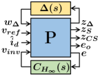
The control system of Fig. 2LABEL:sub@control1 can be realized as a general control configuration as shown in Fig. 2LABEL:sub@control2[26]. It has a generalized MIMO plant, , containing nominal plant models defined as , , , , and with exogenous input signal and output signals . The controller, has input feedback signal, , and output control signal, . The uncertainty function, , with input signal, , and output, is represented using upper linear fractional transformations [26]. The goal is to synthesize the stabilizing controller, , that satisfies the following:
| (8) |
Remark.
Using -iteration algorithm provided in [26] (the state-space solution approach via solving two algebraic Riccati equations), the synthesis of optimal controller is achieved by means of hinfsyn command of MATLAB toolbox. Usually -control algorithms produce controllers of higher order and model reduction becomes essential to design a low order implementable controller. It is achieved by using balanced truncation method removing modes faster than the switching frequency. The resulting controller, , is of the order of which is higher only by orders than that of conventional PR controller with up to order harmonic compensators. Fig. 3LABEL:sub@fig:GZmag and 3LABEL:sub@fig:GZphase corroborate the accomplishment of the objectives by the resulting optimal controller. Moreover, the optimal controller along with the plant results that makes the closed-loop system robust stable. Moreover, robust stability margin is verified by robstab command of MATLAB.
IV Results
SIMULINK/MATLAB simulation studies are carried out for validation. The system parameters used in both the stages are tabulated in Table I. A combination of impedance type and current source type load models are used. However, for closer proximity with practical scenarios, a DC-drive motor load is also considered along with the others and the modelling is followed as mentioned in [23, 27].
| VSI Parameter | Value |
|---|---|
| Rated RMS Output Voltage | (V) |
| Rated Output Frequency () | (rad/s) |
| DC Link Voltage () | (V) |
| Switching Frequency | (kHz) |
| Filter Inductance () | (mH) |
| Filter Capacitance () | (F) |
| Rated Output Power | (kVA) |

|
|
|
|
|
||||||||||
|---|---|---|---|---|---|---|---|---|---|---|---|---|---|---|
| SIMULINK | -based | |||||||||||||
| PR-based[3] | ||||||||||||||
| CHIL | -based |
IV-A Simulation Results and Performance Comparison
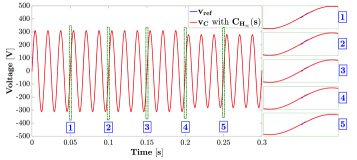
For the purpose of performance comparison, conventional multi-loop-based classical outer PR-based voltage controller and inner PI-based current controller is considered for the time-domain simulation. [3] provides an elaborated guidelines for designing the classical PR and PI based multi-loop voltage controller for grid-forming VSI with enough gain and phase margins. In this work, the guidelines are followed in order to possess a fair comparative study. PI-based inner loop is designed to have phase margin (PM) and gain margin (GM) dB with bandwidth kHz. Similarly, PR-based outer loop is designed to have PM and GM dB with bandwidth kHz. The following sequence of events is used in the MATLAB/SIMULINK-based validation stage.
-
•
VSI is in no-load condition until .
-
•
At , there is a transition from no-load to full-load and stays at full-load condition until .
-
•
At , reactive power drops to until .
-
•
At , both real and reactive power change.
-
•
At , drops and stays until .
-
•
At , VSI is switched to no-load condition.
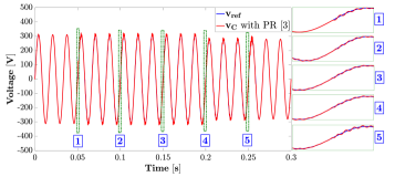
The output voltage waveform of VSI, , during the time-domain events with both proposed -based and conventional-multi-loop-based voltage controller are shown in Fig. 4LABEL:sub@fig:vCHinf and Fig. 4LABEL:sub@fig:vCPR. The enlarged portions in these figures are illustrating the transient behaviors during aforementioned situations. The results substantiate the fact that the proposed -based controller exhibits superior robustness in performance than the multi-loop controller with varying loading conditions. THD of with proposed controller is much smaller than the multi-loop controller with highly non-linear loads (output current is illustrated in Fig. 5). Finally, Table II corroborates the superiority of the proposed controller in reference tracking and disturbance rejection in compare with the classical multi-loop PR-based voltage controller at the cost of increasing the order of controller only by .
IV-B CHIL Simulation Results
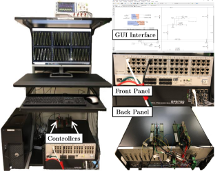
The computational footprint of the proposed -based controller, while implemented in a real low-cost micro-controller board, is an essential check for further validating the performance. Therefore, controller hardware-in-the-loop (CHIL)-based simulation studies are also conducted on OPAL-RT real-time simulator with the proposed -based controller realized on a low-cost Texas-Instruments TMS28379D Delfino controller board as shown in Fig. 6. In similar way, four events are emulated in the OPAL-RT platform and are enlisted as:
-
•
-: A sudden rise in VSI output current, , at with unchanged reference signal, .
-
•
-: A sudden fall in VSI output current, , at with unchanged reference signal, .
-
•
-: A sudden fall in output voltage reference signal, , at with unchanged .
-
•
-: A sudden rise in output voltage reference signal, , at with unchanged .

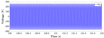
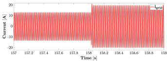
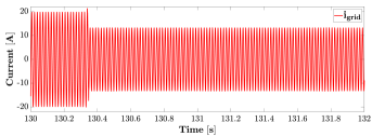
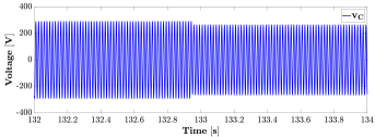
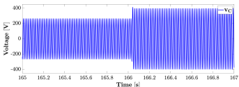

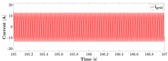
The results for - and - are shown in Fig. 7. It is clearly observed that the output voltage waveforms of VSI, , are insensitive to the sudden changes of (shown in Fig. 7LABEL:sub@fig:igridchil1 and Fig. 7LABEL:sub@fig:igridchil2) in both - and - as shown in Fig. 7LABEL:sub@fig:vCHinfchil1 and Fig. 7LABEL:sub@fig:vCHinfchil2. Similarly, the results for - and - are shown in Fig. 8. It is observed that the output voltage waveforms of VSI, , tracks the changes in reference voltage signal, , very quickly as shown in Fig. 8LABEL:sub@fig:vCHinfchil3 and Fig. 8LABEL:sub@fig:vCHinfchil4 for both - and -. Moreover, due to constant-current type output loads terminated across the VSI, the output current waveform, is unchanged as shown in Fig. 8LABEL:sub@fig:igridchil3 and Fig. 8LABEL:sub@fig:igridchil4. The results shown in Fig. 7 and Fig. 8 clearly substantiate the fact that the dynamic performance of the proposed controller is less sensitive to transients. Moreover, Table II shows that the reference tracking and harmonic rejection performance illustrated in CHIL results are close enough to the results from SIMULINK/MATLAB. However, due to practical and inevitable limitations like quantization error of ADC of the real controller and efficacy of discretization process, the results may differ slightly but under acceptable limit as evidenced in this case also. Along with the performances, this study also showcases the viability of the proposed -based controller in real low-cost control broads.
V Conclusion
This article demonstrates the design and implementation of robust and optimal single-loop voltage controller for single-phase grid-forming VSI. The model uncertainty of VSI imposed by the unknown changing load is demonstrated and its impact on dynamic model of VSI is shown. -based controller design is introduced to address this issue and the required objectives for the optimal controller are discussed to formulate the optimization problem which leads to final optimal controller. A time-domain SIMULINK-based simulation study substantiates the fact that the resulting controller exhibits superior robustness in performance during varying loading of VSI that conventional multi-loop controller architecture. Moreover, OPAL-RT based CHIL simulations are conducted to verify the viability of the resulting controller.
Acknowledgment
The authors acknowledge Advanced Research Projects Agency-Energy (ARPA-E) for supporting this research through the project titled “Rapidly Viable Sustained Grid” via grant no. DE-AR0001016.
References
- [1] J. M. Guerrero, L. Hang, and J. Uceda Antolín, “Control of distributed uninterruptible power supply systems,” IEEE Transactions on Industrial Electronics, vol. 55, no. 8, pp. 2845–2859, 2008.
- [2] J. M. Guerrero, J. C. Vasquez, J. Matas, L. G. De Vicuña, and M. Castilla, “Hierarchical control of droop-controlled ac and dc microgrids—a general approach toward standardization,” IEEE Transactions on industrial electronics, vol. 58, no. 1, pp. 158–172, 2010.
- [3] A. Yazdani and R. Iravani, Voltage-sourced converters in power systems. Wiley Online Library, 2010, vol. 34.
- [4] Y. Wu and Y. Ye, “Internal model-based disturbance observer with application to cvcf pwm inverter,” IEEE Transactions on Industrial Electronics, vol. 65, no. 7, pp. 5743–5753, July 2018.
- [5] J. M. Guerrero, L. G. De Vicuña, J. Miret, J. Matas, and M. Castilla, “Integral control technique for single-phase ups inverter,” in 2002 IEEE International Symposium on Industrial Electronics, ISIE 2002. Institute of Electrical and Electronics Engineers Inc., 2002, pp. 1043–1048.
- [6] J. M. Guerrero, L. G. de Vicuna, J. Miret, J. Matas, and M. Castilla, “A nonlinear feed-forward control technique for single-phase ups inverters,” in IEEE 2002 28th Annual Conference of the Industrial Electronics Society. IECON 02, vol. 1. IEEE, 2002, pp. 257–261.
- [7] H. Wu, D. Lin, D. Zhang, K. Yao, and J. Zhang, “A current-mode control technique with instantaneous inductor-current feedback for ups inverters,” in APEC’99. Fourteenth Annual Applied Power Electronics Conference and Exposition. 1999 Conference Proceedings (Cat. No. 99CH36285), vol. 2. IEEE, 1999, pp. 951–957.
- [8] Q. Lei, F. Z. Peng, and S. Yang, “Multiloop control method for high-performance microgrid inverter through load voltage and current decoupling with only output voltage feedback,” IEEE Transactions on Power Electronics, vol. 26, no. 3, pp. 953–960, 2010.
- [9] D. Dong, T. Thacker, R. Burgos, F. Wang, and D. Boroyevich, “On zero steady-state error voltage control of single-phase pwm inverters with different load types,” IEEE Transactions on Power Electronics, vol. 26, no. 11, pp. 3285–3297, 2011.
- [10] P. C. Loh, M. J. Newman, D. N. Zmood, and D. G. Holmes, “A comparative analysis of multiloop voltage regulation strategies for single and three-phase ups systems,” IEEE Transactions on Power Electronics, vol. 18, no. 5, pp. 1176–1185, 2003.
- [11] M. Prodanovic, “Power quality and control aspects of parallel connected inverters in distributed generation,” Ph.D. dissertation, Imperial College London (University of London), 2004.
- [12] G. Weiss, Q.-C. Zhong, T. C. Green, and J. Liang, “H repetitive control of dc-ac converters in microgrids,” IEEE Transactions on Power Electronics, vol. 19, no. 1, pp. 219–230, 2004.
- [13] T. Hornik and Q.-C. Zhong, “H repetitive voltage control of grid-connected inverters with a frequency adaptive mechanism,” IET power electronics, vol. 3, no. 6, pp. 925–935, 2010.
- [14] T. Hornik and Q. Zhong, “Voltage control of grid-connected inverters based on h and repetitive control,” in 2010 8th World Congress on Intelligent Control and Automation, July 2010, pp. 270–275.
- [15] G. Willmann, D. F. Coutinho, L. F. A. Pereira, and F. B. Líbano, “Multiple-loop h-infinity control design for uninterruptible power supplies,” IEEE Transactions on Industrial Electronics, vol. 54, no. 3, pp. 1591–1602, 2007.
- [16] B. B. Johnson, B. R. Lundstrom, S. Salapaka, and M. Salapaka, “Optimal structures for voltage controllers in inverters,” National Renewable Energy Lab.(NREL), Golden, CO (United States), Tech. Rep., 2018.
- [17] M. Hamzeh, S. Emamian, H. Karimi, and J. Mahseredjian, “Robust control of an islanded microgrid under unbalanced and nonlinear load conditions,” IEEE Journal of Emerging and Selected Topics in Power Electronics, vol. 4, no. 2, pp. 512–520, 2015.
- [18] M. A. U. Rasool, M. M. Khan, Z. Ahmed, and M. A. Saeed, “Analysis of an h robust control for a three-phase voltage source inverter,” Inventions, vol. 4, no. 1, p. 18, 2019.
- [19] J. Teng, W. Gao, D. Czarkowski, and Z.-p. Jiang, “Optimal tracking with disturbance rejection of voltage source inverters,” IEEE Transactions on Industrial Electronics, 2019.
- [20] Z. Li, C. Zang, P. Zeng, H. Yu, S. Li, and J. Bian, “Control of a grid-forming inverter based on sliding-mode and mixed control,” IEEE Transactions on Industrial Electronics, vol. 64, no. 5, pp. 3862–3872, 2016.
- [21] P. Buduma and G. Panda, “Robust nested loop control scheme for lcl-filtered inverter-based dg unit in grid-connected and islanded modes,” IET Renewable Power Generation, vol. 12, no. 11, pp. 1269–1285, 2018.
- [22] Tzann-Shin Lee, S. . Chiang, and Jhy-Ming Chang, “ loop-shaping controller designs for the single-phase ups inverters,” IEEE Transactions on Power Electronics, vol. 16, no. 4, pp. 473–481, July 2001.
- [23] P. Kundur, N. Balu, and M. Lauby, Power System Stability and Control, ser. EPRI power system engineering. McGraw-Hill Education, 1994.
- [24] “IEEE draft standard for the specification of microgrid controllers,” IEEE P2030.7/D10, July 2017, pp. 1–49, Jan 2017.
- [25] “IEEE recommended practice and requirements for harmonic control in electric power systems,” IEEE Std 519-2014 (Revision of IEEE Std 519-1992), pp. 1–29, June 2014.
- [26] I. Postlethwaite, Multivariable Feedback Control: Analysis and Design. New York, NY, USA: John Wiley & Sons, Inc., 1996.
- [27] C. Venkatesh, D. S. Kumar, D. S. Sarma, and M. Sydulu, “Modelling of nonlinear loads and estimation of harmonics in industrial distribution system,” in Fifteenth National Power Systems Conference (NPSC), IIT Bombay, 2008, pp. 592–597.