Isochronous Architecture-Based Voltage-Active Power Droop for Multi-Inverter Systems
Abstract
Advanced microgrids consisting of distributed energy resources interfaced with multi-inverter systems are becoming more common. Consequently, the effectiveness of voltage and frequency regulation in microgrids using conventional droop-based methodologies is challenged by uncertainty in the size and schedule of loads. This article proposes an isochronous architecture of parallel inverters with only voltage-active power droop (VP-D) control for improving active power sharing as well as plug-and-play of multi-inverter based distributed energy resources (DERs). In spite of not employing explicit control for frequency regulation, this architecture allows even sharing of reactive power while maintaining reduced circulating currents between inverters. The performance is achieved even when there are mismatches between commanded reference and power demanded from the actual load in the network. The isochronous architecture is implemented by employing a global positioning system (GPS) to disseminate the clock timing signals that enable the microgrid to maintain nominal system frequency in the entire network. This enables direct control of active power through voltage source inverter (VSI) output voltage regulation, even in the presence of system disturbances. A small signal eigenvalue analysis of a multi-inverter system near the steady-state operating point is presented to evaluate the stability of the multi-inverter system with the proposed VP-D control. Simulation studies and hardware experiments on an 1.2 kVA prototype are conducted. The effectiveness of the proposed architecture towards active and reactive power sharing between inverters with load scenarios are demonstrated. Results of the hardware experiments corroborate the viability of the proposed VP-D control architecture.
Index Terms:
Common-clock/GPS, low-voltage multi-inverter microgrid, virtual impedance, voltage active power droop, voltage source inverterI Introduction
Modernization of rapidly dispatchable DERs to provide demand response and ancillary services are transforming emergent microgrids into advanced microgrids. Advanced microgrids enable additional flexibility, resilience and reliability for local resources as well as support of the large scale grid when connected [1]. These microgrids can be operated in both grid-connected as well as islanded modes. In the islanded mode, DERs support local loads in the microgrid through either centralized, distributed or de-centralized control architectures. Controllers employed either locally at individual DERs or at a microgrid level are responsible for stabilizing microgrid voltage [2], maintaining power quality with plug-and-play capabilities [3], apportioning load between various distributed generations (DGs) [4], and primary frequency response support [5]. A number of hierarchical control schemes achieve one or more of these objectives [6].
A distributed and communication-less approach of controlling inverters is typically achieved through droop control methods. These methods use measurements obtained locally at the DERs and leverage the relationships between system voltage, line frequency, and power supplied by the DERs to ensure regulation of voltage and frequency in the network [7]. In microgrids with high line inductance (high ratio), DERs are generally controlled by conventional and droop control [8, 9], where , , , and are active power, reactive power, frequency, and voltage respectively. The droop strategies in microgrids are motivated by the the autonomous control of synchronous generators, with inherent large rotating inertia directly coupled with the network that primarily rely on conventional droop strategies for regulation of system voltage and frequency. However, low voltage (LV) microgrids use more converter-interfaced DERs, and thus, exhibit low natural inertia with significant ratio because of the small spatial expanse of the networks [10]. Consequently, non-conventional and droop control strategies [10, 11] have gained attention for LV microgrids with the advantages of direct voltage control [12] and improved harmonic power sharing [13] compared to conventional droop control. Moreover, in order to improve transient performance and leverage decoupling compensations for droop controlled MMG, there are several works in the literature concentrating on modifying the droop characteristic equations [14, 15, 16, 17, 18]. However, these more complicated droop characteristic equations are difficult to analyze, give stability guarantees and difficult to incorporate in applications.
In traditional droop based strategies, with the frequency related droop strategy employed, deviation of microgrid frequency caused by mismatches between load and generation is inevitable. Here, LV microgrids with low inertia converter-interfaced DERs, the frequency may deviate considerably from nominal [8, 19, 20]. Typically, a secondary controller, operating at a slower time-scale than the autonomous droop based response, utilizes communication between DERs to restore the steady state system frequency to nominal [21]; however, it is difficult to mitigate the transient frequency deviation caused by sudden load changes especially in islanded microgrids. This regulation becomes even more difficult in the presence of uncertain renewable energy resources along with the added complexity of synchronizing DERs in a parallel inverter network. Other limitations in traditional droop methods arise from the trade-offs between accurate power sharing on one hand and the desire for stringent regulation of system voltage and frequency on the other. These trade-offs result from mismatches in the commanded reference power and actual load as well as the output impedance of VSI and line parameters resulting in large circulating currents.
In this article, we propose using only VP-D control for voltage regulation and address frequency regulation by providing a common timing signal from a GPS receiver to all the inverters. This enables generation of a common frequency reference for all the inverters and avoids the need for explicit frequency control; moreover, the framework obviates the need for communication between inverters. In contrast to existing GPS-based methods [22, 23], our approach simultaneously achieves multiple objectives including reduced circulating currents between VSIs with better voltage regulation, reduced complexity due to the absence of PLL required for frequency synchronization. Accordingly, the main contributions of the proposed isochronous architecture are summarized as follows.
1) Access to common clock pulses in this architecture enables operation of the Multi-inverter MicroGrid (MMG) at a single frequency even in the presence of system disturbances. VP-D control decouples voltage regulation objectives from frequency variations thereby alleviating issues such as frequency dependent control resulting in poor voltage regulation and poor disturbance rejection. This architecture also enables improved start up transients, reduced circulating currents between participating VSIs and easy plug-and-play of VSIs in the MMG.
2) The architecture does away with issues stemming from active frequency-regulation in full-droop methods. VP-D control allows direct control of active power with regulation of voltage magnitude. The resulting control law guarantees that the parallel inverters share reactive power such that deviations from desired reactive power sharing remain bounded while serving a common load even without explicitly controlling the reactive power flow. The resulting controller design is simpler because no explicit control is required.
3) The proposed framework facilitates a comprehensive analysis that provides: i) delineation analytically of how circulating current between VSIs depends on output voltage regulation error; ii) small-signal based stability analysis of the ac microgrid by having access to the common clock signal to generate components without added complexities of PLL dynamics. These provide useful design guidelines for selecting droop gains and virtual output resistances to maintain system stability
Results show that the proposed architecture exhibits improved transients over full-droop implementations during start-up and different plug-and-play scenarios. For scenarios with symmetric active, reactive power sharing, an improvement of is observed in the magnitude of circulating current between any two inverters, reactive power sharing ratio accuracy improved from to be within of desired and transient response time from 0.1238 s to 0.02 s. Voltage regulation error at PCC improved from to (of nominal) during plug-and-play of the MMG.
Experimental results are provided for a system of two 0.6 kVA inverters under different load variations and sharing ratios to validate the feasibility and effectiveness of the proposed isochronous architecture.
The rest of the paper is organized as follows. Section II describes the system and control architecture. Section III provides analytical results for the multi-inverter system, and Section IV presents simulation and experimental validation on a two-inverter microgrid network. Finally, Section V summarizes observations and insights that highlight this work.
II System Description and Controller Design
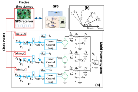
This section provides the details of an LV resistive MMG network containing parallel VSIs, serving a common load, , connected at a single point of common coupling (PCC) as shown in Fig. 1. Each inverter in the MMG includes a communication module that receives synchronized clock pulses from the GPS segment [24] through a GPS receiver. These clock pulses are then used by the proposed outer VP-D control to provide a synchronized sinusoidal reference voltage signal to inner-loop controllers located at each VSI forming the isochronous system architecture. We begin our discussion by describing first the dynamics of the single inverter system and the controllers employing the proposed control law for achieving output voltage regulation and load disturbance rejection through a cascaded multi-loop control architecture.
II-A Single Inverter System with multi-loop control design
A single phase H-bridge inverter with an output filter is connected to load through a line resistance . The VSI is modeled as a controllable voltage source, , by employing an average model of the inverter [25]. The dynamics of the VSI are described as:
where , , , and are average values over one switching cycle () of control signal, inductor current, output voltage, and output current, respectively (See Fig. 2). Taking a Laplace transform of these equations and eliminating , the open-loop averaged output voltage dynamics of the inverter are given as,
| (1) |
The control design objectives are to: i) regulate the output voltage of the inverter () to track a reference signal (); ii) regulate the output inductor current of the inverter () to track a reference signal (); iii) reject disturbances due to load variations. We propose the following control law for the inverter:
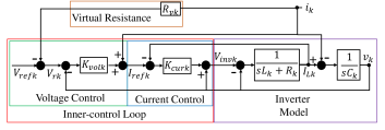
| (2) |
where , , and . As shown in Fig. 2, the control law takes the form of cascaded voltage and current controllers.The outer voltage controller, , acts on a sinusoidal reference signal provided by the outer droop law with the incorporation of a voltage drop, , on a virtual resitance, . A feed-forward of the line current is used to minimize inrush currents and improve the transient response of the outer voltage controller. The output of the voltage controller, , provides the sinusoidal reference current signal to be tracked by the inductor current which generates the controllable voltage signal, , for the VSI. The main advantages of the inner-outer loop structure are the decoupled design of the fast inner current controller and the slow outer voltage controller as well as the increased robustness of the VSI to load variations. By combining (1) and (2), the closed-loop averaged output voltage dynamics of inverter are given by:
| (3) |
where , is the sensitivity transfer function, is the complementary transfer function, and
. Note that,
is the equivalent Thevenin output impedance of the inverter at the fundamental frequency, rad/s.
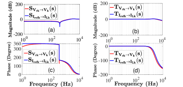
The primary control objectives thus translate to for voltage regulation and the closed-loop inner- current loop transfer function from to be such that and for rejecting the effects of load disturbances (See Fig. 3).
The current-control and voltage-control designs are based on the internal model principle [25, 26], where the controllers and are designed to have poles and loop-shaping-based design to cancel the pole located at by the current controller. Moreover, this design ensures proper separation in bandwidth of both the controllers (current control loop has the larger bandwidth), which enables the inner current loop to make the inductor current to track the reference current .
An output virtual resistance loop [13] is also adopted to alleviate the sensitivity of active power sharing to the line and output impedances. This can be achieved by designing the virtual resistance, , to dominate the line impedance of the VSI, rendering the design insensitive to line and filter parameters. However, is bounded above to ensure VSI output voltage regulation to be within prescribed limits as larger results in larger regulation error by reducing .
Assumption 1.
The proposed control design shown in Fig. 2 satisfies the following properties:
-
1.
and are sinusoidal with frequency .
-
2.
has poles at , that is, is a factor in .
-
3.
The closed-loop system from reference voltage, , to output voltage, , is stable.
The following theorem shows that if all external inputs (i.e., and ) to the system are sinusoidal with frequency , then the inverter voltage follows the sinusoidal reference with zero steady-state error.
Theorem 1.
Proof.
See Appendix. ∎
II-B Outer Voltage-Active Power Droop
The sinusoidal voltage reference signal, , used by the inner multi-loop controllers is generated by the proposed VP-D control law. The proposed droop law does not facilitate any explicit control on reactive power () unlike full droop control methodologies where active and reactive power are controlled separately by controlling voltage and frequency respectively. The VP-D law for the VSI is
| (4) |
where , , , , and are inverter output voltage magnitude, reference output voltage magnitude, droop coefficient, measured output active power, and reference active power of the inverter. Here, . To control , it is necessary to measure . This is usually achieved by measuring instantaneous power (i.e., ) and passing it through a first order low pass filter (LPF) with bandwidth which is designed to be much smaller than the voltage control loop. Reference [27] proposes a framework for obtaining a near-exact solution for determining the active power for a single VSI serving a load.
II-C Isochronous Architecture
An isochronous architecture can be achieved by providing a common timing signal to all inverters in the network. The advantages of such an architecture over frequency droop are delineated earlier in this article. GPS is used to obtain absolute time, time interval and frequency with precision up to a nanosecond (ns). GPS receiver modules have the ability to measure high precision timing signals which are readily available and inexpensive. This makes them an ideal candidate for time synchronization applications. It is assumed here that there is accurate and precise synchronization of the real-time clocks of the networked distributed devices to the common clock and that the clock synchronization protocol is in compliance with IEEE 1588-2008 standards [28].
It is imperative that such an architecture be robust to any momentary loss of access to the common clock by one or more inverters in the system. Such a protocol is assumed and its mitigation is not a point of discussion for this article. However, mitigation of such scenarios can be achieved by employing a corrective mechanism, for example by employing a local clock at each VSI for satisfactory operation. This is possible since a local clock can provide a reasonable estimate of GPS time signal for tens of seconds, eventually shifting the operating point in response to load changes causing degradation in power system performance. For conditions of continued signal loss, the VSI unit cannot participate in system wide load sharing and should be isolated from the rest of the system. Methodologies such as radio reference signal could be used if there is sufficient concern about system wide loss of GPS reference signal [29]. Similarly, [30] utilizes three different PLL structures to guarantee robustness versus delay or loss in communication to synchronize the phase and the frequency of all of the devices connected to the microgrid.
III Multi-Inverter System Isochronous Operation
III-A Performance of Individual Inverters
In this section, the performance of the multi-inverter system with the proposed VP-D approach is analyzed. A benefit of the VP-D approach is that reactive power sharing among individual inverters is maintained within a bound without having control of reactive power explicitly defined as a control objective. Theorem 2 provides analytical expressions for output voltage and line currents of networked VSI units.
Theorem 2.
Proof.
See Appendix. ∎
Corollary 2.1.
In the case of purely resistive load ,i.e., , the steady state voltage and current at the output of the inverter are and for . In other words, phase lags .
Proof.
From the expression of in Theorem 2, it can be clearly stated that if , then is a pure real number and thus . Therefore,
∎
Remark 2.1.
III-B Design Guideline for Droop Coefficients
In the following theorem the phase difference between inverter currents and is characterized in the general setting for complex linear loads.
Theorem 3.
Let Suppose the conditions of Assumption 1 hold, then the phase of differs from the phase of , given as,
| (5) |
Proof.
See Appendix. ∎
Remark 3.1.
For purely resistive load, as becomes real. This also follows from Corollary 2.1.
Corollary 3.1.
Suppose and then,
Proof.
Assuming that are small so that: , it follows that
where is the power factor of the load . ∎
Remark 3.2.
Corollary 3.1 extends the relationship in (5) to show that to ensure the phase difference in the inverter currents to be small, the values have to be close to Indeed, for the phase difference of the currents to be smaller than , it follows that needs to be satisfied, where is the p.f. of the load, . Moreover, when compared to the branch resistance, , and virtual resistance, , are both designed small. Thus, the assumptions in Corollary 3.1 are not restrictive.
Remark 3.3.
The expression for depends only on , whereas all other parameters are load and network parameters. Moreover, the deviation of from is dictated by the outer droop law. Thus, this analysis aids the appropriate choice of and the allowable mismatch from the reference active power that is to be delivered, E.g., selecting droop gains for any two inverters , such that will keep reactive power flows in check.
III-C Stability Analysis
One of the important aspects to be investigated for the multi-inverter system operation is its stability. The non-linear multi-inverter closed-loop system can be represented as,
| (6) |
where denotes states of the system including both physical variables and internal control variables as shown in Table I and the input to the system, is . The objective is to develop a small signal model of the multi-inverter system by linearizing the system (6) around a stable operating point. We consider the axis as the local reference frame for the VSI operating at a rotating frequency . The individual VSI state equations are derived in terms of their individual local reference frame. The local reference frames are transformed to the global reference (D-Q) frame which is chosen to be the PCC reference frame operating at . This allows for generalizing the VP-D architecture beyond single-phase microgrids. We first consider the state equations of individual VSIs in their local reference frames represented by , where represents the synchronous reference frame angle at PCC and represents the deviation of the VSI from the synchronous reference frame (Fig. 1 b). The translation between local frame to global D-Q frame is given by,
We consider,
where, . and are the components of a given state . For the single phase case, . Note that having access to the common clock signal facilitates generation of components without added complexities of a PLL implementation. This is given by the following transformation matrix,
Note that in the case of perfect synchronization with the GPS clock signal, for all VSI as a result of which all inverters can be represented in the reference frame eliminating the need for translating each VSI’s states into the common reference frame. Each of these VSI units comprise an outermost droop control, inner multi-loop voltage and current controllers, output LC-filter connected to the PCC through line impedances and are terminated at the common load. Combining these dynamics, the small signal state space model of the single inverter system is given as,
| (7) |
where ,
and is given as (),
| Parameters | States |
|---|---|
| Droop & LPF | |
| Voltage Controller | |
| Current Controller | |
| LC filter | |
| Line parameters | |
| Load, |
Combined model of the N inverter system can now be written as [31, 32],
| (8) |
where
,
and .
Considering the dynamics of the lumped complex () load and considering only a resistive load for simplicity, we obtain:
| (9) |
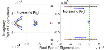
Thus, using (9) in (8) we get, where, is a matrix that captures the coupling of VSI interconnection at PCC. Stability analysis in the presence of a complex load can be obtained in a similar manner. The stability analysis of the system is given by the eigenvalues of . For a two inverter setup the eigenvalues of the system are shown in Fig. 4 setup configured with the parameters of Table II. The results are obtained for the case of an asymmetric power sharing ratio of 2.2. The line paramerters are chosen to be and .
Remark 3.4.
The small signal stability analysis reveals that the stability of the system is maintained in the VP-D architecture when deviation, , for all individual VSI units with respect to the common reference frame are . The presence of larger inductive loads (low power factor) results in driving the eigenvalues of the linearized system towards the origin.
IV Results
| Parameters | Values |
|---|---|
| Cut off frequency () | |
| Nominal Voltage at PCC | 120 V |
| Nominal Frequency at PCC () | 60 Hz |
| Branch Resistance | 0.2 |
| Inverter DC Link Voltage | 250 V |
| Inverter Filter Inductance | 0.063 mH |
| Inverter Filter Capacitance | 1 |
| Rated Power of | 0.6 kVA |
| Rated Power of | 0.6 kVA |
IV-A Simulation Results
To validate the viability of VP-D-based control of a multi-inverter system, a MATLAB/SIMULINK-based switching model of two inverters sharing a common load at PCC in a LV resistive network is simulated. The network and inverter parameters used in the simulation are listed in Table II. Fig. 5 shows the voltage and current output results from a simulation where two parallel inverters are serving a common load of 0.58 kVA with (lagging). Both inverters are operated with and . Fig. 5(a) shows that the share between two inverters, i.e., , is maintained at 1.07. Note here that without having a separate control strategy, the reactive power sharing between the inverters is nearly even. Here, is 0.88. The mismatch between actual measured and reference output active power for both the inverters, primarily because of finite line losses, results in a small voltage deviation from (around -0.5) at the PCC. The voltage waveform at the PCC and the output current are shown in Fig. 5(b). Fig. 5(c) shows the circulating current between the two inverters, which is significantly low compared to the rated output current.
IV-A1 Mismatched line parameters
Simulations for a number of scenarios are considered each for symmetric as well as asymmetric active power sharing between the two inverters with mismatched reference and injection values of active power for the two inverters. Total reference power commanded from each inverter is kW whereas the actual load, , is a series - load with and H. for both inverters. The obtained reactive power share is , when the line resistance of inverter 2, satisfies . For the cases when the line resistances are highly mismatched ( i.e., ), , is 0.868 with a worst-case sharing ratio of 0.735 obtained when . This result demonstrates the performance of the proposed architecture in worse-case conditions toward mismatches in active power references and line parameter.
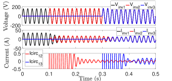
IV-A2 Plug-and-play capability
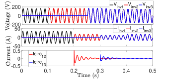
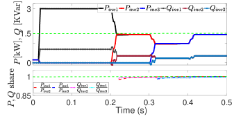
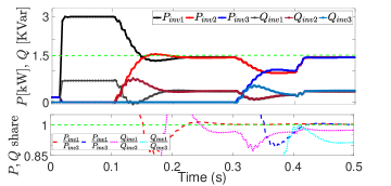
A three VSI network is considered. At s VSI-1 is on and synchronized with the local clock signal serving a load, . At s and s, VSI-2 and VSI-3 set individual clock receive flags high respectively to receive synchronized clock pulses for reference generation. The output voltages at the capacitor of VSI-2 and VSI-3 are thus generated at these instants. In order to demonstrate the plug and play capability, VSI-2 is connected to the common load and VSI-1 at s and VSI-3 is then connected to the rest of the network at s. Symmetric power sharing is desired at all VSIs. Output voltages, line currents and circulating currents are shown in Fig. 7. Fig. 8 shows the symmetric sharing of the load, , with active power sharing ratio of 1 as well as reactive power sharing ratio of at steady state even when no control is implemented. Finally, at s, a load transition to 4.5 kW (0.97 p.f.lagging) occurs.
IV-A3 Comparison with full droop ()
The three VSI network as above is considered while implementing a full droop architecture with and droop laws. At s VSI-1 is on and serving a load, . At s and s, VSI-2 and VSI-3 are synchronized and connected to the network. The presence of an integrator in the droop implementation results in initial transients in output voltage and current of the VSIs that cause in higher transient and steady state circulating currents. This is apparent at s and s when the VSIs are turned on (see Fig. 9). At s, a load transition to 4.5 kW (0.97 p.f.lagging) occurs. The full droop implementation also suffers from longer transient times to reach steady state in both active and reactive power sharing as well as poor reactive power sharing ratio (sharing ratio of 1 is desired) during load changes and steady state values due to mismatch in commanded and actual reactive power (see Fig. 10). Meanwhile, the isochronous architecture provides improved transient and steady state performance during black starts, plug-and-play of VSIs and load changes even in mismatched conditions. High power sharing accuracy during plug-and-play and fast transient response demonstrates the superiority of the proposed architecture over full droop methods in MMGs.
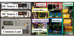
IV-B Experimental Validation
Experiments are carried out in a laboratory setup as shown in Fig. 6. The experimental configuration consists of two single-phase insulated-gate bipolar transistor-based H-bridge inverter units along with output filter and controller unit for each, a purely resistive network, a variable common load served by both inverter units, and a Raspberry Pi-based (RPi) clock pulse generator. The RPi unit provides clock pulses with precise time-stamping. Each inverter consists of a digital input module to emulate a GPS receiver. All inverters synchronize their local clocks, using zero-crossing detection and pulse counting, to the RPi clock signal transmitted as a square wave. This clock signal is then used to generate sinusoidal references to individual inner-loop controllers. Each inverter unit is rated as 0.6 kVA operating and utilizing a switching frequency of 20 kHz. The active power control including active power calculation and droop control, reference voltage generation, inner voltage and current controller, and PWM generation, digital input module are implemented on a TMS320F28335 digital signal processor. The inverter and network parameters are provided in Table II. The value of the droop coefficients for both inverters i.e., are selected as V/W. The loop-shaping controllers and are designed as described in Section II-A with bandwidths 980 Hz and 600 Hz, respectively, for closely tracking sinusoidal references.
The expressions of and are as follows:
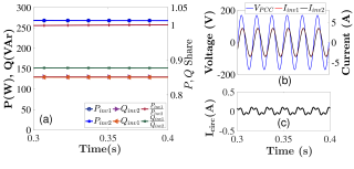
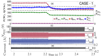
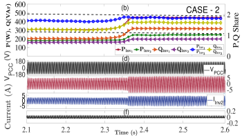
To verify the proposed VP-D control of the multi-inverter system, two case studies are conducted for experimental validation of the active and reactive power sharing performance (as shown in Fig. 11) using the hardware prototype. Case 1 considers two inverters serving a common load of = 0.87 kVA with transition at t = 2.22 s to = 0.61 kVA maintaining unity power factor throughout. Meanwhile, Case 2 studies two inverters serving a common load of = 0.6 kVA with transition at t = 2.34 s to = 0.84 kVA maintaining 0.8 power factor throughout.
In Case 1, both inverters are assigned with asymmetric active power references of = 0.56 kW and = 0.31 kW throughout the operation. The active power sharing ratio of is maintained throughout the operation, as shown in Fig. 11(a). Moreover, the output reactive powers of both the inverters are zero, which is a direct validation of Corollary 2.1. The transient time of the inverter, which here is defined as the 90% settling time of the inverter’s output current peak after a load step, is about 0.037 s (i.e., 2.2 cycles of 60 Hz). This demonstrates the ability of the proposed controller to inject real power into the network to provide ancillary support to the microgrid in fast- (primary response) timescale regimes. Fig. 11(c) shows the voltage and output current waveforms of both inverters before and after the load transition. There is a finite active power mismatch () that causes a deviation () of voltage magnitude at the PCC from its nominal value. These deviations are attributed to measurement error in active power at relatively low power operating conditions. Fig. 11(e) illustrates the circulating current between two inverters throughout the operation [33]. Clearly, the magnitude of the circulating current is significantly less than the nominal output current ratings of the inverters. The total harmonic distortion (THD) values of the voltage waveform at the PCC before and after the transition are 1.86% and 1.47%. These values are also maintained within acceptable standards [34]. Similarly, in Case 2, the inverters are assigned asymmetric active power references of = 0.3 kW and = 0.18 kW throughout the operation. The sharing ratio of active power is maintained at 1.67 throughout the operation. Moreover, reactive power is shared with a ratio of without implementing any dedicated control strategies throughout the operation. Fig. 11(d) illustrates the voltage and output current waveforms of both inverters before and after the load transition. The transient time of inverter current is 0.05 s (i.e., 2.99 cycles of 60 Hz). Here, that results in a deviation () in PCC voltage magnitude from its nominal. Fig. 11(f) illustrates the circulating current between the two inverters.
IV-C Design Considerations of Multi-Inverter System
This section provides design guidelines to restrict limits on reactive power flows for implementing VP-D control in a multi-inverter system.
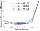
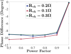
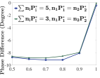
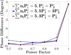
Fig. 12 shows experimental results for the variation in phase difference (inverter currents) when an electronic load ( Fig. 6), with apparent Power kVA is varied in power factor from to unity. It is important to emphasize here that even with such a low power factor of the load to be served and no explicit control over reactive power flows of the system, the phase difference between currents is maintained low ( or less) by the proposed controller architecture.
Fig. 12(a) and Fig. 12(b) show that higher values of branch resistance and virtual resistance lead to smaller phase differences. This, however, may lead to a decrease in the accuracy of active power sharing in the network.
From Fig. 12(c) and Fig. 12(d) it can be observed that a choice of smaller results in a smaller phase difference. These observations serve as design considerations to limit reactive power flows and implement an isochronous VP-D architecture in an LV multi-inverter system.
V Conclusion
In this paper, a voltage-active power half-droop was proposed and demonstrated to show high power sharing accuracy during plug-and-play and fast transient response of the proposed architecture over full-droop methods in a resistive LV ac microgrid. A loop shaping-based control law was designed for a single inverter unit to enable close regulation of the reference sinusoidal voltage signal to be tracked. A novel isochronous architecture was also proposed to maintain the system frequency and enable active power sharing in the multi-inverter system. The main advantage of the proposed architecture is to keep the reactive power flows small among the inverters without implementing an explicit droop law, thereby, reducing the overall complexity of the inverter controllers. Small signal based stability analysis was conducted to show the feasibility of the proposed architecture for various scenarios of the multi-inverter system. Moreover, analytical results were derived to provide design guidelines for selecting droop gains when there are active power mismatches and uncertainties in the load present in the LV microgrid. Experimental results were provided for various scenarios that validate the performance and capabilities of the proposed controller architecture.
Appendix
Proof of Theorem 1: The steady-state tracking error is:
Now, formulated in (3) can be written as:
Suppose has poles at Hence, can be factored as Thus, because has a pole at , it is evident that will have a numerator with a factor This implies that Also, from the final value theorem, it follows that:
In a similar manner, we can rewrite the expression of as:
Since , it follows that Also, from the final value theorem, it follows that:
As the term has a factor it follows that
This implies that in steady state the output of inner-loop controller tracks the input sinusoidal reference with zero error.
V-A Extension for Multiple Inverter System
The closed-loop averaged output voltage dynamics of (3) can be extended for inverters and described by:
| (10) |
where, , , , and . Assuming a linear load, the closed-loop expression of and can be formulated by using the admittance matrix , as follows:
| (11a) | ||||
| (11b) | ||||
where , , , and . In a similar way, can be formulated by rewriting in matrix form:
| (12) |
where , , .
Proof of Theorem 2: For clarification, .
Also, can be written as , where is the Laplace transform of a sinusoid with frequency .
Using the Woodbury matrix identity and matrix manipulation:
Thus, it follows that for the inverter in the steady state:
where:
By denoting = and = ,
Now, from Theorem 1:
Proof of Theorem 3: From the expression of deduced in the previous proof. Now, :
where . Note that:
References
- [1] S. Marzal, R. Salas, R. González-Medina, G. Garcerá, and E. Figueres, “Current challenges and future trends in the field of communication architectures for microgrids,” Renewable and Sustainable Energy Reviews, vol. 82, pp. 3610–3622, Feb. 2018.
- [2] J. C. Vasquez, R. A. Mastromauro, J. M. Guerrero, and M. Liserre, “Voltage support provided by a droop-controlled multifunctional inverter,” IEEE Transactions on Industrial Electronics, vol. 56, no. 11, pp. 4510–4519, 2009.
- [3] F. Blaabjerg, R. Teodorescu, M. Liserre, and A. V. Timbus, “Overview of control and grid synchronization for distributed power generation systems,” IEEE Transactions on industrial electronics, vol. 53, no. 5, pp. 1398–1409, 2006.
- [4] S. Patel, S. Attree, S. Talukdar, M. Prakash, and M. V. Salapaka, “Distributed apportioning in a power network for providing demand response services,” in IEEE International Conference on Smart Grid Communications (SmartGridComm), Oct. 2017, pp. 38–44.
- [5] B. Lundstrom, S. Patel, S. Attree, and M. V. Salapaka, “Fast Primary Frequency Response using Coordinated DER and Flexible Loads: Framework and Residential-scale Demonstration,” in IEEE Power Energy Society General Meeting (PESGM), Aug. 2018, pp. 1–5.
- [6] J. M. Guerrero, J. C. Vasquez, J. Matas, L. G. de Vicuna, and M. Castilla, “Hierarchical Control of Droop-Controlled AC and DC Microgrids—A General Approach Toward Standardization,” IEEE Transactions on Industrial Electronics, vol. 58, no. 1, pp. 158–172, Jan. 2011.
- [7] M. C. Chandorkar, D. M. Divan, and R. Adapa, “Control of parallel connected inverters in standalone AC supply systems,” IEEE Transactions on Industry Applications, vol. 29, no. 1, Jan. 1993.
- [8] J. M. Guerrero, L. G. De Vicuna, J. Matas, M. Castilla, and J. Miret, “Output impedance design of parallel-connected ups inverters with wireless load-sharing control,” IEEE Transactions on industrial electronics, vol. 52, no. 4, pp. 1126–1135, 2005.
- [9] W. Yao, M. Chen, J. Matas, J. M. Guerrero, and Z.-M. Qian, “Design and analysis of the droop control method for parallel inverters considering the impact of the complex impedance on the power sharing,” IEEE Transactions on Industrial Electronics, vol. 58, no. 2, pp. 576–588, 2011.
- [10] T. Vandoorn, B. Meersman, J. De Kooning, J. Guerrero, and L. Vandevelde, “Automatic power sharing modification of p/v droop controllers in low-voltage resistive microgrids,” IEEE Transactions on Power Delivery, vol. 27, no. 4, pp. 2318–2325, 2012.
- [11] C. K. Sao and P. W. Lehn, “Control and power management of converter fed microgrids,” IEEE Transactions on Power Systems, vol. 23, no. 3, pp. 1088–1098, 2008.
- [12] A. Engler and N. Soultanis, “Droop control in LV-grids,” in 2005 International Conference on Future Power Systems, Nov. 2005, p. 6.
- [13] J. M. Guerrero, J. Matas, L. Garcia de Vicuna, M. Castilla, and J. Miret, “Decentralized Control for Parallel Operation of Distributed Generation Inverters Using Resistive Output Impedance,” IEEE Transactions on Industrial Electronics, vol. 54, no. 2, pp. 994–1004, Apr. 2007.
- [14] N. M. Dehkordi, N. Sadati, and M. Hamzeh, “Robust tuning of transient droop gains based on kharitonov’s stability theorem in droop-controlled microgrids,” IET Generation, Transmission & Distribution, vol. 12, no. 14, pp. 3495–3501, 2018.
- [15] Z. Afshar, M. Mollayousefi, S. M. T. Bathaee, M. T. Bina, and G. B. Gharehpetian, “A novel accurate power sharing method versus droop control include autonomous microgrids with critical loads,” IEEE Access, vol. 7, pp. 89 466–89 474, 2019.
- [16] D. K. Dheer, Y. Gupta, and S. Doolla, “A self adjusting droop control strategy to improve reactive power sharing in islanded microgrid,” IEEE Transactions on Sustainable Energy, 2019.
- [17] Z. Peng, J. Wang, D. Bi, Y. Wen, Y. Dai, X. Yin, and Z. J. Shen, “Droop control strategy incorporating coupling compensation and virtual impedance for microgrid application,” IEEE Transactions on Energy Conversion, vol. 34, no. 1, pp. 277–291, 2019.
- [18] R.-J. Wai, Q.-Q. Zhang, and Y. Wang, “A novel voltage stabilization and power sharing control method based on virtual complex impedance for an off-grid microgrid,” IEEE Transactions on Power Electronics, vol. 34, no. 2, pp. 1863–1880, 2018.
- [19] J. Rocabert, A. Luna, F. Blaabjerg, and P. Rodríguez, “Control of power converters in ac microgrids,” IEEE Transactions on Power Electronics, vol. 27, no. 11, pp. 4734–4749, Nov 2012.
- [20] R. Majumder, A. Ghosh, G. Ledwich, and F. Zare, “Angle droop versus frequency droop in a voltage source converter based autonomous microgrid,” in 2009 IEEE Power Energy Society General Meeting, Jul. 2009, pp. 1–8.
- [21] Q. Shafiee, J. M. Guerrero, and J. C. Vasquez, “Distributed secondary control for islanded microgrids - a novel approach,” IEEE Transactions on power electronics, vol. 29, no. 2, pp. 1018–1031, 2014.
- [22] M. S. Golsorkhi, D. D.-C. Lu, and J. M. Guerrero, “A gps-based decentralized control method for islanded microgrids,” IEEE Transactions on Power Electronics, vol. 32, no. 2, pp. 1615–1625, 2017.
- [23] S. Riverso, F. Sarzo, G. Ferrari-Trecate et al., “Plug-and-play voltage and frequency control of islanded microgrids with meshed topology.” IEEE Trans. Smart Grid, vol. 6, no. 3, pp. 1176–1184, 2015.
- [24] H. Packard, “Gps and precision timing applications,” application note 1272, Tech. Rep., 1996.
- [25] A. Yazdani and R. Iravani, Voltage-Sourced Converters in Power Systems. Hoboken, NJ, USA: John Wiley & Sons, Inc., Jan. 2010.
- [26] Y. W. Li, “Control and Resonance Damping of Voltage-Source and Current-Source Converters With LC Filters,” IEEE Transactions on Industrial Electronics, vol. 56, no. 5, pp. 1511–1521, May 2009.
- [27] S. Salapaka, B. Johnson, B. Lundstrom, S. Kim, S. Collyer, and M. Salapaka, “Viability and analysis of implementing only voltage-power droop for parallel inverter systems,” in 53rd IEEE Conference on Decision and Control, Dec. 2014, pp. 3246–3251.
- [28] “IEEE standard for a precision clock synchronization protocol for networked measurement and control systems,” IEEE Std 1588-2008, pp. 1–300, July 2008.
- [29] R. Majumder, B. Chaudhuri, A. Ghosh, R. Majumder, G. Ledwich, and F. Zare, “Improvement of stability and load sharing in an autonomous microgrid using supplementary droop control loop,” IEEE transactions on power systems, vol. 25, no. 2, pp. 796–808, 2009.
- [30] A. Bellini, S. Bifaretti, and F. Giannini, “A Robust Synchronization Method for Centralized Microgrids,” IEEE Transactions on Industry Applications, vol. 51, no. 2, pp. 1602–1609, Mar. 2015.
- [31] N. Pogaku, M. Prodanovic, and T. C. Green, “Modeling, analysis and testing of autonomous operation of an inverter-based microgrid,” IEEE Transactions on power electronics, vol. 22, no. 2, pp. 613–625, 2007.
- [32] M. Rasheduzzaman, J. A. Mueller, and J. W. Kimball, “An accurate small-signal model of inverter-dominated islanded microgrids using reference frame,” IEEE Journal of Emerging and Selected Topics in Power Electronics, vol. 2, no. 4, pp. 1070–1080, 2014.
- [33] M. Zhang, B. Song, and J. Wang, “Circulating current control strategy based on equivalent feeder for parallel inverters in islanded microgrid,” IEEE Transactions on Power Systems, vol. 34, no. 1, pp. 595–605, 2018.
- [34] “IEEE standard for interconnection and interoperability of distributed energy resources with associated electric power systems interfaces,” IEEE Std 1547-2018, pp. 1–138, April 2018.